High Quality GeSn Layer with Sn Composition up to 7% Grown by Low Temperature Magnetron Sputtering for Optoelectronic Application
Jiayin Yang1, Huiyong Hu1, Yuanhao Miao1*, Linpeng Dong2,3, Bin Wang1, Wei Wang4,5 ,Han Su1, Rongxi Xuan1, Heming Zhang1
1Key Laboratory of Wide-Gap Semiconductor Materials and Devices, School of Microelectronics, Xidian University, Xi’an710071, China
2Guangdong Provincial Key Laboratory of Optical Fiber Sensing and Communications, Jinan University, Guangzhou, 510632, China
3Department of Optoelectronic Engineering, Jinan University, Guangzhou, 510632, China
4School of Physics and Electronic Information, Yunnan Normal University, Kunming, 650500, China
5Yunnan Key Laboratory of Opto-electronic Information Technology, Kunming, 6505 00, China
*Corresponding author: [email protected]
Abstract
In this paper, we have used magnetron sputtering to grow the high-quality GeSn
layer on Ge (100) with Sn compositin up to 7%. The crystallinity of the GeSn layer is
pretty good, and the strain relaxation degree of the GeSn layer is evaluated to be
approximately 50%. The root mean square (RMS) value is 0.8 nm, and the averaged
TDDs in the GeSn layer is 8.7×109 cm-2, which is obtained from the rocking curve of
GeSn layer along (004) plane. PL measurement result shows the significant optical
emission from the deposited high-quality GeSn layer, which also means that
magnetron sputtering is an optional way to achieve the higher Sn composition GeSn
luminescent material. To verify whether our deposited GeSn can used for
optoelectronic devices, we fabricate the simple vertical p-i-n diode, and the room
temperature current-voltage (I-V) characteristic was obtained. This result paves the
way for future sputtered-GeSn optimization, which is critical for the optoelectronic
application.
Keywords: GeSn layer; averaged TDD; magnetron sputtering; p-i-n diode
Introduction
Recently, GeSn alloys have the capability to become a direct bandgap material at
an certain Sn composition of around 6%-10% [1-3], making it a possible candidate as
the optical gain medium in group IV light source [4-6]. Besides, GeSn is also a
complementary metal-oxide-semiconductor (CMOS) compatible optoelectronic
material for Si photonics, which makes it more attractive. The epitaxial growth of
high Sn composition GeSn with high material quality is challenging due to the solid
solubility of Sn in Ge or Ge in Sn is less than 1%, and the smaller surface free energy
of Sn than that of Ge makes Sn more likely immigrates to the surface of the GeSn
film during epitaxial growth and thermal treatment [7-11]. So far, several techniques,
such as CVD [12-14], MBE [15-17], and magnetron sputtering [18-22] have been
employed to achieve the crystalline GeSn layers.
RPCVD has grown high-quality GeSn with Sn content up to 12.6% using Ge2H6
and SnCl4 as precursors, which has led to the first demonstration of optical pumped
GeSn laser [23]. The lasing of GeSn micro-disks with 16% Sn content has also
achieved by using the same precursors [24]. At the same time, GeH4 and SnCl4 have
also utilized to grown high-quality GeSn with Sn content up to 17%, which also
contribute to the achievement of GeSn laser with the wavelength coverage of 2-3um
and the lasing temperature of 180K[25]. Besides, high order Ge hydrides such as
Ge3H8 and Ge4H10 were also utilized to pursue high Sn content GeSn layers
[26-28].High-quality GeSn thin film with high Sn content (22.3%) was deposited on
Sn graded GeSn buffer and optically pumped lasing has also been observed at the
wavelength of 3um and lasing temperatures of 150K and 180K[29-31].
SiGeSn/GeSn/SiGeSn QW laser on Si with Sn content up to 14.4% has also been
achieved, which features a higher maximum operating temperature of 90K and lower
lasing thresholds of 25 and 62kW/cm2 at 10 and 77K. MBE has grown high-quality
GeSn, which contributes to the demonstration of GeSn light emitting diodes (LEDs)
[33-36]and photodetectors[37-39]. However, GeSn laser has not been reported yet,
which is mainly due to the lower Sn composition of the GeSn layer deposited by
Comparing with CVD and MBE, magnetron sputtering is also an alternative
method to grow GeSn alloys. So far, only a few groups have grown crystalline GeSn
alloys. High-quality GeSn layer was grown on a Ge (100) substrate by magnetron
sputtering, which contributes to the first demonstration of GeSn p-i-n photodetectors
[18]. High-quality SiGeSn/GeSn multiple quantum well (MQW) structure was also
grown on Ge substrate by sputtering epitaxy, and Sn content of the GeSn layer is 6%,
which contributes to the demonstration of GeSn photodetector[22]. In addition,
crystalline GeSn thin films with high Sn content (28%) were also deposited on Sn
graded GeSn buffer by sputtering epitaxy [20]. Our previous work has shown the
deposition of GeSn on tensile-strained Ge buffer with low Sn content (3%), and room
temperature photoluminescence spectrum has also been observed [21]. However, no
room temperature photoluminescence spectrum and GeSn-based diode were reported
for a higher Sn composition GeSn alloy deposited by this method. Besides, we
propose a novel method to obtain the TDDs in GeSn layers from GeSn (004) rocking
curves.
In this work, we have grown high-quality GeSn layer on Ge (100) substrate with
Sn composition up to 7%. Room temperature optical emission from the GeSn layer is
observed and averaged TDDs in the layer is also obtained from the rocking curve
along (004) plane. To further verify the material quality of the film, we have
fabricated simple vertical GeSn p-i-n diode.
Methods
Preparation of GeSn layers
GeSn epitaxial layer was deposited in physical vapor deposition (PVD) system
manufactured by Kurt J. Lesker Corporation. High pure Ge target (99.999%) and Sn
target (99.999%) were employed to deposit the GeSn layer on a Ge substrate. To
prevent excess heating, the Ge target and Sn target were bonded to a copper baking
plate. GeSn layer with Sn content up to 7% was deposited directly on Ge (100)
substrate by magnetron co-sputtering, and Ge wafer was n-doped. At first, Ge wafer
was prepared by dipping in a mixture of H2O2 and H2O for a few seconds and the
oxide layer was removed by dipping in HF. This procedure was repeated several times
to ensure the removal of several atomic layers of Ge. After cleaning, the Ge wafer was
loaded into PVD growth chamber and the chamber was pumped down to 10-6 mTorr
as the base pressure. The substrate was heated to 160℃ before the deposition of GeSn
film. During the deposition, sputtering pressure was kept at 3mTorr by utilizing argon.
The composition of Ge and Sn in the film was controlled by maintaining an RF power
of 120W for the Ge target and varying the RF power of Sn target. The deposition rate
is about 0.2-0.5nm/s, and the evaluated thickness of the GeSn layer is approximately
400nm.
Fabrication of simple GeSn diode
After the deposition of GeSn layer, B implant (dose of 4×1015cm-2 and energy of
40keV) was performed to dope the 400nm i-GeSn, followed by RTA in N2 to activate
the p-type dopant concentration. Then, the p-i-n diode was metallization processed
and RTA treatment. The schematic cross section of the layer structure of the sample is
shown in Fig.1 (a). In order to form a simple GeSn p-i-n diode, we have cut the sample into small pieces of 0.8mm×0.8mm square using laser slicing. Then, the
typical I-V characteristic of the sample was measured by Keithley 4200
semiconductor characterization system parameter analyzer.
Fig.1 (a) The schematic cross section of the layer structure of the sample, (b) dicing diagram of the sample
Characterization method for GeSn layer
The crystallinity quality of the GeSn layer was determined by high-resolution
N-type Ge substrate Ni 50nm i-GeSn layer 350nm P-GeSn layer 40-50nm
Al 300nm Al 300nm Ni 50nm
…...
…...
…...
X-ray diffraction (HR-XRD) measurement. Sn composition of the GeSn layer was
verified by energy dispersive spectrometer (EDS). The XRD 2theta-ω scans along
(004) plane and (224) plane were accomplished. Rocking curve of GeSn (004) was
also carried out to determine the averaged threading dislocation densities (TDDs) in
the GeSn layer. PL was used to determine the band gap edge. PL setup consists of a
Fourier transform infrared spectroscopy (FTIR), liquid nitrogen (LD2) cooled InGaAs
detector, 532nm continuous wave (CW) laser, and a grating monochromator.
Results and discussion
Crystallinity, Sn content, and strain of GeSn layer
64.0 64.5 65.0 65.5 66.0 66.5 67.0 100 101 102 103 104 105 106 107 108
(a) (004) Scan
GeSn Peak 65.18°
XR
D Intensi
ty
2Theta-Omega(°) Ge Peak
81.0 81.5 82.0 82.5 83.0 83.5 84.0 84.5 85.0 100 101 102 103 104 105 106
(b) (224) Scan
Ge Peak
XRD Intensity
2Theta-Omega(°) GeSn Peak 82.98°
Fig.2 High resolution 2Theta-omega XRD scans of the GeSn alloy along (a) (004) plane, (b) (224) plane
The GeSn layer was grown on Ge (100) substrate by magnetron co-sputtering
using high pure Ge target (99.999%) and Sn target (99.999%). The thickness of the
GeSn layer was evaluated to be 400nm. High-resolution X-ray diffraction (HR-XRD)
measurement was used to assess the crystallinity quality and Sn content of the
epitaxial layer. Fig.2 (a) shows the XRD 2theta-omega (004) scan of the sample, in
which the diffraction peak of GeSn and Ge can be seen. The peaks at 66° and 65.18°
correspond to the Ge substrate and GeSn layer, respectively. The out-of-plane lattice
constant of the GeSn layer was extracted from the following expression:
1 004 2 sin x x Ge Sn a ⊥ (1)
peak of the GeSn layer along (004) plane. Hence, the out-of-plane lattice constant of
the GeSn layer is calculated to be 5.721A. Fig.2 (b) shows the XRD 2theta-omega
(224) scan of the sample, in which the diffraction peak of GeSn and Ge can also be
clearly seen. The peaks at 83.1° and 82.98° respond to the Ge substrate and GeSn
layer, respectively. The in-plane lattice constant of the GeSn layer can be reckoned as:
1
1
1/2
||
2 2
224
8
1 16
x x
x x
Ge Sn
Ge Sn
a
d a
⊥
(2)
where d224 is the crystal spacing. For the XRD scan along (224), d224 can be calculated
using the equation:
2 sin
hkl
hkl
d
, (3)
Therefore, d224 of the GeSn layer is estimated to be 1.162A. Substituting the value of
d224 into eq.(2), the in-plane lattice constant of the GeSn layer is calculated to be
5.634A.
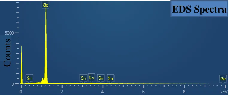
Fig.3 Surface energy dispersive spectrometer (EDS) spectra of the GeSn layer
To further determine the Sn content of the GeSn layer, we have carried out the
surface EDS spectra of the GeSn layer. The spectra image was obtained from typical
EDS analysis. Fig. 3 shows that 7 primary peaks are formed at 0.4, 1.3, 3, 3.4, 4.4, 10, and 11keV. The peaks at 0.4, 3, 3.4 and 4.4keV match the spectral lines of Sn.
Furthermore, the peaks at 1.3, 10, and 11keV match spectral lines of Ge. It was
confirmed that Sn composition of the GeSn layer is estimated to be 7%. Based on the
EDS Spectra
lattice elastic theory, bulk lattice constant of GeSn (abulk) can be obtained using the
following equation:
12
// 11
2C =
C
bulk bulk
a a
a a
⊥ (4)
where a⊥ is the out-of-plane lattice constant of the GeSn layer, a/ / is the in-plane
lattice constant of the GeSn layer, C11 and C12 are the elastic coefficient. Besides,
there is a relationship between C11, C12, and the Sn composition of the GeSn [40]:
11 2
12
0.3738 0.1676 0.0296 C
x x
C (5)
We can first substitute the Sn composition (7) obtained from EDS into Eq.(5), and the
value of C11/C12 is calculated to be 0.0966. abulk can also be calculated using the
in-plane lattice constant of the GeSn layer, out-of-plane lattice constant of the GeSn
layer, and the value of C11/C12 (0.0966). The bulk lattice constant of the GeSn is
calculated to be 5.707A.
Therefore, the relaxation degree can be demonstrated as:
GeSn //
GeSn
GeSn Ge bulk
a a
R
a a
⊥ (6)
where Ge
a is the lattice constant of the Ge (aGe= 5.658A), a⊥ is the out-of-plane
lattice constant of the GeSn, a/ / is the in-plane lattice constant of the GeSn, and
bulk
a bulk lattice constant of GeSn. Finally, the relaxation degree of the GeSn layer is
evaluated to be approximately 50%.
30 31 32 33 34 35 100
101 102 103 104 105 106 107 108
32.5926°
XR
D Intens
ity
Diffraction Peak Position(°) (004) Rocking Curve
Fig.4 Rocking curve of GeSn layer along (004) plane
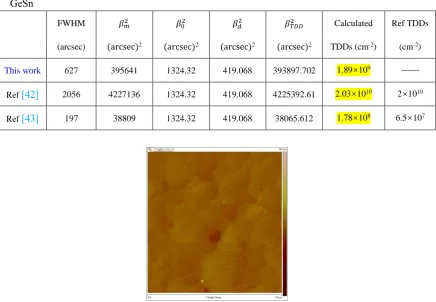
By now, transmission electron microscope (TEM) and etching pit density (EPD)
have been utilized to evaluate the TDDs in GeSn layers. However, it is difficult to
determine the dislocation density of the material using EPD when the dislocation
density is more than 106cm-2. Moreover, TEM also has its regional limitation because
TEM can only obtain the TDDs of the material in a small region. So, we evaluate the
TDDs of GeSn layer by rocking curve. High-resolution x-ray diffraction (HR-XRD)
patterns are recorded on a Phillips X’Pert diffractometer operating at 40 mA and 40
kV with using Cu Kα1 radiation. From our previous report [41], the intrinsic FWHM
of strained GeSn can be described as:
(6)
where rc is the radius of the electron,is the wavelength of the X-ray,is the Bragg
angle,| F |hkl is the reflection structure factor for the (hkl),a0is the lattice constant of the bulk GeSn, andis the angle between the crystal surface and the diffracting planes.
The reflection structure factor for the GeSn (004) are all 64f 2, where f is the dispersion factor of an atom.
The FWHM broadening by the TDDs in GeSn layer can represented as:
2 2 2 2
0
(hkl) (hkl) (hkl)
TDD m d
(7)
where 𝛽𝑚 is the measured FWHM of the strained GeSn, 𝛽0 is the intrinsic FWHM
2
1/2
3
0
(hkl)
[r
c
(1 | cos 2 |) | F |] [sin(
hkl
) / sin(
)]
/ [
a
0
sin(2 )]
of the strained GeSn, and 𝛽𝑑 is the FWHM broadening by incident beam divergence
of the instrument.
The averaged TDDs in the strained GeSn layer can be written as an empirical
formula:
2 2
/ 2 ln 2
TDD
D b (8)
The value of b is 0.4. The calculated values of 𝛽𝑚2, 𝛽02, 𝛽𝑑2, 𝛽𝑇𝐷𝐷2 , and TDDs of
GeSn layer are outlined in Table I. In addition, we compare the calculated TDDs with other results, which is closely consistent with the Ref TDDs.
Table I. Comparison of the calculated values of 𝛽𝑚2, 𝛽02, 𝛽𝑑2, 𝛽𝑇𝐷𝐷2 , TDDs, and Ref TDDs for
GeSn
FWHM
(arcsec)
𝛽𝑚2
(arcsec)2
𝛽02
(arcsec)2
𝛽𝑑2
(arcsec)2
𝛽𝑇𝐷𝐷2
(arcsec)2
Calculated
TDDs (cm-2)
Ref TDDs
(cm-2)
This work 627 395641 1324.32 419.068 393897.702 1.89×10⁹ ——
Ref [42] 2056 4227136 1324.32 419.068 4225392.61 2.03×10¹⁰ 2×10¹⁰
Ref [43] 197 38809 1324.32 419.068 38065.612 1.78×10⁸ 6.5×10⁷
Fig.5 5μm×5μm AFM image of the GeSn layer deposited by magnetron sputtering
In order to determine the surface morphology of the GeSn layer, AFM
measurement was performed. Fig.5 shows the typical 5μm×5μm AFM image of the GeSn layer and RMS value of the GeSn sample was extracted from AFM scans. The
as-grown GeSn layer shows a smooth surface and root-mean-squared (RMS) value is
1600 1800 2000 2200 2400 0
1x10³ 2x10³ 3x10³
4x10³ 5x10³
6x10³
PL Intensity
Wavelength(nm) 1870nm
Fig.6 Room temperature PL spectra of the GeSn layer deposited by magnetron sputtering
The photoluminescence (PL) characterization was undertaken to examine the
optical property of the GeSn layer. The PL measurement was excited by a continuous
wave (CW) laser with 532nm wavelength. During the excitation of the laser, the laser
beam was focused to be a 100um spot and the power was modulated to be 500mW.
The PL emission was collected (LN2) by a Fourier transform infrared spectroscopy
(FTIR), which is equipped with liquid nitrogen (LN2) InGaAs detector. Fig.6 shows the room temperature PL spectra of GeSn layer and the peak at 1870nm shows that
GeSn layer is indirect bandgap material [1].
-4 -2 0 2 4
1E-5 1E-4 1E-3 0.01 0.1 1
Curre
nt
Dens
ity
(A/cm
3 )
Voltage(V)
Fig.7 (a) Current-voltage (I-V) characteristic setup, (b)Room temperature current-voltage (I-V) characteristic of an 8mm×8mm square p-i-n diode with GeSn layer deposited by magnetron sputtering
temperature. The electrical property of the p-i-n diode was performed using a Keithley
4200 semiconductor characterization system parameter analyzer. Fig.7 (b) shows the typical I-V characteristic of an 8mm×8mm square p-i-n diode with the GeSn layer
deposited by magnetron sputtering. The very high dynamic resistance may be
attributed mainly to the fact that Si wafer and Ge substrate have a high series resistor.
Ultimately, we can conclude that the sputter doposited GeSn layer has the great
potential to be used for the fabrication of optoelectronic devices.
Conclusions
In summary, high-quality GeSn layer with Sn content up to 7% was successfully
grown on the Ge (100) substrate via magnetron sputtering. The crystallinity of the
GeSn layer is pretty good, and the strain relaxation degree in the layer is approximate
50%. The RMS value is only 0.8 nm, and the averaged TDDs in the GeSn layer is
evaluated to be 8.7×109 cm-2 along (004) plane. PL measurement result shows the
optical emission from the deposited high-quality GeSn layer. Besides, the fabricated
vertical p-i-n device exhibit good room temperature current-voltage (I-V)
characteristic. From the results, we conclude that sputter deposited GeSn have the
potential to achieve high Sn composition GeSn layer with proper design, which is
critical for the optoelectronic application.
Acknowledgement
This research is supported by the Natural Science Foundation of China (Grant No. 61704130 and No. 61474085), Science and Technology on Analog Integrated Circuit Laboratory (Grant No.6142802180206), Fundamental Research Funds for the Central Universities (Grant No.20101196823), and Science Research Plan in Shaanxi Province of China (Grant No.2019GY-019 and 2018JQ6064). Dr. Miao would also like to thank the support from the Fundamental Research Funds for the Central Universities, and the Innovation Fund of Xidian University.
References
with 2230 nm photoluminescence[J]. Applied Physics Letters, 2014, 105(15): 151109.
[2] Stange D, Wirths S, von den Driesch N,etal.Optical Transitions in Direct-Bandgap Ge1–xSnx Alloys[J]. ACS Photonics, 2015, 2(11): 1539-1545.
[3] Ryu M Y, Harris T R, Yeo Y K, et al. Temperature-dependent photoluminescence of Ge/Si and Ge1-ySny/Si, indicating possible indirect-to-direct bandgap transition at lower Sn content [J]. Applied Physics Letters, 2013, 102(17): 171908.
[4] Oehme M, Werner J, Gollhofer M, et al. Room-temperature electroluminescence from GeSn light-emitting pin diodes on Si[J]. IEEE Photonics Technology Letters, 2011, 23(23): 1751-1753.
[5] Zhou Y, Dou W, Du W, et al. Systematic study of GeSn heterostructure-based light-emitting diodes towards mid-infrared applications[J]. Journal of Applied Physics, 2016, 120(2): 023102.
[6] Stange D, Von Den Driesch N, Rainko D, et al. Study of GeSn based heterostructures: towards optimized group IV MQW LEDs [J]. Optics express, 2016, 24(2): 1358-1367.
[7] Li H, Cui Y X, Wu K Y, et al. Strain relaxation and Sn segregation in GeSn epilayers under thermal treatment[J]. Applied Physics Letters, 2013, 102(25): 251907.
[8] Li H, Chang C, Chen T P, et al. Characteristics of Sn segregation in Ge/GeSn heterostructures[J]. Applied Physics Letters, 2014, 105(15): 151906.
[9] Tsukamoto T, Hirose N, Kasamatsu A, et al. Investigation of Sn surface segregation during GeSn epitaxial growth by Auger electron spectroscopy and energy dispersive x-ray spectroscopy[J]. Applied Physics Letters, 2015, 106(5): 052103.
[10] Wang W, Li L, Zhou Q, et al. Tin surface segregation, desorption, and island formation during post-growth annealing of strained epitaxial Ge1− xSnx layer on Ge (0 0 1) substrate[J]. Applied Surface Science, 2014, 321: 240-244.
[11] Miao Y H, Hu H Y, Song J J, et al. Effects of rapid thermal annealing on
crystallinity and Sn surface segregation of films on Si (100) and Si (111)[J]. Chinese Physics B, 2017, 26(12): 127306.
[12] Margetis J, Mosleh A, Al-Kabi S, et al. Study of low-defect and strain-relaxedGeSn growth via reduced pressure CVD in H2 and N2 carrier gas[J]. Journal of Crystal Growth, 2017, 463: 128-133.
[13]Grant P C, Dou W, Alharthi B, et al. UHV-CVD Growth of High Quality GeSn Using SnCl4: From Growth Optimization to Prototype Devices[J]. arXiv preprint arXiv:1810.02523, 2018.
[14] Dou W, Alharthi B, Grant P C, et al. Crystalline GeSn growth by plasma enhanced chemical vapor deposition [J]. Optical Materials Express, 2018, 8(10): 3220-3229.
[15] Gupta S, Chen R, Magyari-Kope B, et al. GeSn technology: Extending the Ge electronics roadmap[C] Electron Devices Meeting (IEDM), 2011 IEEE International. IEEE, 2011: 16.6. 1-16.6.4.
strained GeSn alloys up to 12.5% Sn [J]. Journal of crystal growth, 2013, 384: 71-76.
[17]Yu K, Zhao Y, Li C, et al. The Growth of GeSn Layer on Patterned Si Substrate by MBE Method [J]. ECS Transactions, 2018, 86(7): 349-355.
[18]Zheng J, Wang S, Liu Z, et al. GeSn pin photodetectors with GeSn layer grown by magnetron sputtering epitaxy[J]. Applied Physics Letters, 2016, 108(3): 033503.
[19]Tsukamoto T, Hirose N, Kasamatsu A, et al. Formation of GeSn layers on Si (001) substrates at high growth temperature and high deposition rate by sputter epitaxy method[J]. Journal of Materials Science, 2015, 50(12): 4366-4370.
[20] Zheng J, Liu Z, Zhang Y, et al. Growth of high-Sn content (28%) GeSn alloy films by sputtering epitaxy [J]. Journal of Crystal Growth, 2018, 492: 29-34.
[21] Miao Y, Wang Y, Hu H, et al. Characterization of crystalline GeSn layer on tensile-strained Ge buffer deposited by magnetron sputtering [J]. Materials Science in Semiconductor Processing, 2018, 85: 134-140.
[22] Zheng J, Wang S, Cong H, et al. Characterization of a Ge1− x− ySi ySn x/Ge1− x Sn x multiple quantum well structure grown by sputtering epitaxy[J]. Optics letters, 2017, 42(8): 1608-1611.
[23] Wirths S, Geiger R, Von Den Driesch N, et al. Lasing in direct-bandgap GeSn alloy grown on Si[J]. Nature photonics, 2015, 9(2): 88.
[24]Reboud V, Gassenq A, Pauc N, et al. Optically pumped GeSn micro-disks with 16% Sn lasing at 3.1 μ m up to 180 K[J]. Applied Physics Letters, 2017, 111(9): 092101.
[25] Margetis J, Al-Kabi S, Du W, et al. Si-Based GeSn Lasers with Wavelength Coverage of 2–3 μm and Operating Temperatures up to 180 K[J]. ACS Photonics, 2017, 5(3): 827-833.
[26] Grzybowski G, Jiang L, Beeler R T, et al. Ultra-low-temperature Epitaxy of Ge-based semiconductors and Optoelectronic structures on Si (100): Introducing higher order Germanes (Ge3H8,Ge4H10)[J]. Chemistry of Materials, 2012, 24(9): 1619-1628.
[27] Grzybowski G, Beeler R T, Jiang L, et al. GeSn alloys on Si using deuterated stannane and trigermane: synthesis and properties [J]. ECS Transactions, 2013, 50(9): 865-874.
[28]Xu C, Gallagher J D, Senaratne C, et al. CMOS compatible in-situ n-type doping of ge using new generation doping agents P (MH3)3 and As(MH3)3 (M= Si, Ge)[J]. ECS Transactions, 2015, 69(14): 3-15.
[29] Dou W, Zhou Y, Margetis J, et al. Optically Pumped GeSn-edge-emitting Laser with Emission at 3 µm for Si Photonics[C]CLEO: Applications and Technology. Optical Society of America, 2018: AF1Q. 5.
[30] Dou W, Zhou Y, Margetis J, et al. Optically pumped lasing at 3 μm from compositionally graded GeSn with tin up to 22.3%[J]. Optics letters, 2018, 43(19): 4558-4561.
Growth[J]. Scientific reports, 2018, 8(1): 5640.
[32]Margetis J, Zhou Y, Dou W, et al. All group-IV SiGeSn/GeSn/SiGeSn QW laser on Si operating up to 90 K [J]. Applied Physics Letters, 2018, 113(22): 221104.
[33] Oehme M, Kostecki K, Arguirov T, et al. GeSn heterojunction LEDs on Si substrates[J]. IEEE Photonics Technology Letters, 2014, 26(2): 187-189.
[34]Oehme M, Werner J, Gollhofer M, et al. Room-temperature electroluminescence from GeSn light-emitting pin diodes on Si[J]. IEEE Photonics Technology Letters, 2011, 23(23): 1751-1753.
[35] Schwartz B, Oehme M, Kostecki K, et al. Electroluminescence of GeSn/Ge MQW LEDs on Si substrate[J]. Optics letters, 2015, 40(13): 3209-3212.
[36] Gupta J P, Bhargava N, Kim S, et al. Infrared electroluminescence from GeSn heterojunction diodes grown by molecular beam epitaxy[J]. Applied Physics Letters, 2013, 102(25): 251117.
[37]Su S, Cheng B, Xue C, et al. GeSn pin photodetector for all telecommunication bands detection[J]. Optics express, 2011, 19(7): 6400-6405.
[38]Oehme M, Schmid M, Kaschel M, et al. GeSn pin detectors integrated on Si with up to 4% Sn[J]. Applied Physics Letters, 2012, 101(14): 141110.
[39]Zhang D, Xue C, Cheng B, et al. High-responsivity GeSn short-wave infrared pin photodetectors[J]. Applied Physics Letters, 2013, 102(14): 141111.
[40] Chang G E, Basu R, Mukhopadhyay B, et al. Design and modeling of GeSn-based heterojunction phototransistors for communication applications[J]. IEEE Journal of Selected Topics in Quantum Electronics, 2016, 22(6): 425-433.
[41] Miao Y H, Hu H Y, Li X, et al. Evaluation of threading dislocation density of strained Ge epitaxial layer by high resolution x-ray diffraction [J]. Chinese Physics B, 2017, 26(12): 127309.
[42] Tsukamoto T, Hirose N, Kasamatsu A, et al. Formation of GeSn layers on Si (001) substrates at high growth temperature and high deposition rate by sputter epitaxy method[J]. Journal of Materials Science, 2015, 50(12): 4366-4370.