Available online:
http://edupediapublications.org/journals/index.php/IJR/
P a g e | 1083Design And Implementation Of Low Power Combinational Circuits
On FPGA Using Reversible Encoder And Decoder In Vivado
Mr P.Karthik & Mr.S.K. Satyanarayana
1
department Of Electronics And Communication Engineering ,Vlsi&Es,Sreenidhi Institute Of Science
And Technology.
Yamnampet,Ghatkesar, Hyderabad,Telangana,
-
501301
2
department Of Electronics And Communication Engineering ,Assistant Professor,Sreenidhi Institute Of
Science And Technology.
Yamnampet,Ghatkesar,Telangana,
-
501301
.
ABSTRACT:
In the present emerging field for the research the reverse logic is one of the most demanding and helpful concept. The main purpose of this paper is to realize various types of combinational circuits like adder, multiplexer..etc using reversible encoder and decoder circuits with minimum quantum cost. There are many reversible logic gates like Fredkin gate, Feynman gate, Double Feynman gate, Peres gate, Seynman gate etc. The concept is explained using the reversible encoder and decoder by making use of Fredkin gates and Feynman gates with minimum quantum cost. The reversible logic can be explained as the logic in which the number of output lines are equal to the number of input lines and using all the bits in the circuit.ie. there are n-input and k- output Boolean function F(X1,X2,X3….Xn) is said to be reversible if and only if (i) n is equa l to k,(ii)each input pattern is mapped uniquely to the output pattern. The gate must run forward and backward which means the inputs can be retrieved from the outputs. Thus when the device obeys these two conditions the second law of thermodynamics guarantee that the device dissipates very low amount of heat. Thus the Fan-Out and Feedback are not allowed in logical reversibility. In recent days ,the reverse logic is used in its applications like Qunatum Computing, Optical Computing, Nano-Technology, Low Power VLSI. Thus the main feature of it being the property of Low Power Consumption.The circuit has been Designed, Simulated and Implemented using VIVADO Software.
KEYWORDS: Fredkin gates, Feyman gates, Peres gate Quantum Cost, Garbage Outputs. Reverse logic gates, Low Power, VIVADO Software
.
I.
INTRODUCTIONReversible logic is an emerging field for research in the present era. The aim of this paper is to realize different types of combinational circuits with low power consumption by using reverse logic gate. Reversible Logic finds its own application in Quantum computing, Nanotechnology, optical
computing, computer graphics and low Power VLSI. Ralf Launduer told that heat dissipation in circuits is not because of the process involved in the operation, but it is due to the bits that were erased during the process. He introduced that losing of a single bit in the circuit causes the smallest amount of heat in the computation which is equal to KTln2 joules where K is Boltzmann constant and T is Temperature. The amount of heat dissipated in simple circuits is very small but it becomes large in the complex circuits which imply propagation delay also. Later in 1973 C. H. Bennett H. Bennett described that the Power dissipation due to the bit loss can be overcome if each and every computation in circuit was carried out in reversible manner. Quantum networks are designed of quantum logic gates. As each gate perform a unitary operation, KTln2 Joules energy dissipation wouldn’t occur if the computation is carried out in reversible manner. Thus computation done in reversible manner doesn’t require erasing of bits. The amount of heat dissipated in the system holds a direct relationship to the number of bits erased or lost during the computation.
.
II.
PROBLEM STATEMENTThe Design of Combinational and Sequential Circuits has been going on in research for the past few years. Various proposals were given for the design of combinational circuits like adders, subtractors, multiplexers, decoders etc., the existing method consists design of 4x16 decoder whose Quantum Cost is less than the previous design. Replacing fredkin gates for designing 2×4 decoder reversible gates like peres gate, TR gate, NOT gate and CNOT gate are used. The whole design is done using Fredkin, CNOT, Peres gates which give better Quantum Cost when compared to the other reversible Logic gates. The number of gates required to design 4x16 decoder are 18 in which there are 12 fredkin gates, one peres gate, one TR gate, one NOT gate and 3 CNOT gates. The sum of all the quantum costs of each gate gives total quantum cost of 4x16 decoder and 16x4 encoder.Thus by using all these reverse gates all or total no of bits in the circuit and being used and the hence, the power consumption of the circuit is being reduced.
Available online:
http://edupediapublications.org/journals/index.php/IJR/
P a g e | 1084 The Reversible Logic involves the use of Reversible Gatesconsists of the same number of inputs and outputs i.e., there should be one to one mapping between input vectors and output vectors. And they can be made to run backward direction also. Certain limitations are to be considered when designing circuits based on reversible logic (i) Fan out is not permitted in reversible logic and (ii) Feedback is also not permitted in reversible logic. In Reversible logic using outputs we can obtain full knowledge of inputs. Reversible logic conserves information. Some cost metrics like Garbage outputs, Number of gates, Quantum cost, constant inputs are used to estimate the performance of reversible circuits. Garbage outputs are the extra outputs which help to make inputs and outputs equal in order to maintain reversibility. They are kept alone without performing any operations. Number of gates count is not a good metric since more number of gates can be taken together to form a new gate. Quantum Cost is the number of elementary or primitive gates needed to implement the gate. It is nothing but the number of reversible gates (1×1 or 2×2) required to construct the circuit. Delay is one of the important cost metrics. A Reversible circuit design can be modeled as a sequence of discrete time slices and depth is summation of total time slices. In Digital Electronics the binary decoder is a combinational logic circuit that converts the binary integer value to the associated output pattern. Various proposals are given to design of combinational and sequential circuits in the undergoing research.
a) Reversible Logic Gates:
The basic Reversible Logic Gates present in the literature are briefed below. The gates that are suitable for the design with optimum quantum cost can be selected.
1.NOT GATE:The NOT GATE is the simple Reversible Logic gate. It is 1×1 Reversible Logic Gate with the quantum cost zero. The Not gate simply shifts the complementary of the input to output as shown in the figure1. It is the basic primitive gate which may involve in construction of reversible logic gate, thus owing its own importance in determining the quantum cost of designed Reversible logic gate.
Fig. 1 NOT Gate And Its Truth Table
2.FEYNMAN GATE (FG): Feynman gate is a 2×2 reversible gate as shown in below figure2. The Feynman gate is also called as CNOT gate i.e., controlled NOT gate.
The Feynman gate is used to duplicate of the required outputs since Fan-out is not allowed in reversible logic gates. The Quantum Cost of FG is 1. This is also the primitive gate owing its importance in determining quantum cost metric.
Fig. 2 Feynman Gate And Its Truth Table
3.DOUBLE FEYNMAN GATE (DFG):Double Feynman Gate is a 3×3 reversible gate. The outputs are defined as shown in the below figure3. The quantum cost of DFG is 2. This gate can also be used for duplicating outputs.
Fig:3 Double Feynman Gate And Its Truth Table
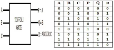
4.TOFFOLIGATE:(TG)Toffoli Gate is 3×3 reversible gate. The outputs are defined as shown in the below figure4. The Quantum Cost of TG is 4.
Fig.4 Toffoli Gate And Its Truth Table
5.FREDKIN GATE:(FDG) Fredkin Gate is a 3×3 reversible gate. The outputs are defined as shown in the below figure4. The Quantum Cost of FDG is 5. This paper mainly surrounds around Fredkin gate.
Available online:
http://edupediapublications.org/journals/index.php/IJR/
P a g e | 10856.PERES GATE (PG):Peres Gate is a is a 3×3 reversible gate. The outputs are defined as shown in the below figure6. The Quantum Cost of PG is 4.
Fig.6 Peres Gate And Its Truth Table
7.TR GATE: TR Gate is a 3×3 reversible gate. The outputs are defined as shown in the below figure7. The quantum cost of TRG gate is given by 4.
Fig.7 TR Gate And Its Truth Table
b) Basic Gates Using Reversible Gates:
Considering our circuit requirements ,the need is to design AND gate and OR gate using reversible gates. Here we used fredkin gate to design AND and OR gates as shown in figure8. Importance is given to fredkin gate because it gives optimistic performance at less Quantum Cost for designing AND and OR gates.
Fig.8 And Gate Using Fredkin And Or Gate Using Fredkin
IV. PROPOSED METHOD
Different Reversible Encoder(4x2,8x3,16x4) and Decoder circuits like (2×4, 3×8, 4×16 )are designed using Fredkin Gates (mainly), Feynman gates and Peres gate, TR gate. Some combinational circuits like adder, multiplexer etc., are designed using these reverse Encoder and reverse Decoders. The concept of duplicating a single output to required number of outputs using Feynman gate is introduced where Fan-out was not allowed in reversible computation. Thus by doing so and applying timing constraints to the circuit the power consumption is effectively reduced and the circuit run more faster and efficiently than the previous obtained results. The main aim of this paper is to reduce the power consumption and to use all the bits in the circuit effectively leaving no bit unused.
Fig 9: Circuit Diagram Of Reversible 4×16 Decoder
Available online:
http://edupediapublications.org/journals/index.php/IJR/
P a g e | 1086 Fig11: Circuit Diagram Of Adder CircuitFig12: Circuit Diagram Of Multiplexer Using Decoder
1.1.1.Third-order Headings. Third-order headings, as in this paragraph, are discouraged. However, if you must use them, use 10-point Times, boldface, initially capitalized, flush left, preceded by one blank line, followed by a period and your text on the same line.
2.
Acknowledgements
This work was supported in part by a grant from the National Science Foundation.
3.
References
List and number all bibliographical references in 9- point Times, single-spaced, at the end of your paper. When referenced in the text, enclose the citation number in square brackets, for example [2-4], [2, 5], and [1].
[1] Briand, L. C., Daly, J., and Wüst, J., "A unified framework for
coupling measurement in objectoriented systems", IEEE
Transactions on Software Engineering, 25, 1, January 1999, pp. 91-121.
[2] Maletic, J. I., Collard, M. L., and Marcus, A., "Source Code Files as Structured Documents", in Proceedings 10th IEEE International Workshop on Program Comprehension (IWPC'02), Paris, France, June 27-29 2002, pp. 289-292.
[3] Marcus, A., Semantic Driven Program Analysis, Kent State University, Kent, OH, USA, Doctoral Thesis, 2003.
[4] Marcus, A. and Maletic, J. I., "Recovering Documentation-to-Source-Code Traceability Links using Latent Semantic Indexing", in Proceedings 25th IEEE/ACM International Conference on Software Engineering (ICSE'03), Portland, OR, May 3-10 2003, pp. 125-137.
V.
SIMULATION RESULTS OF PROPOSED CIRCUITSa)4×16 Reverse Decoder
Fig.10 RTL Schematic Of 4×16 Reversible Decoder
Fig.11 Simulated Output For 4 ×16 Decoder
Available online:
http://edupediapublications.org/journals/index.php/IJR/
P a g e | 1087 output power has been reduced which makes the systemmore efficient and high throughput value can be obtained using minimum quantum costs in the circuit.
Fig.12 Implementation Output For 4 ×16 Decoder
Fig.13 Output Power For 4 ×16 Decoder
b) 16×4 Reverse Encoder
Fig.14 RTL Schematic Of 16×4 Reversible Encoder
Fig.15 Simulated Output For 16 ×4 Encoder
Available online:
http://edupediapublications.org/journals/index.php/IJR/
P a g e | 1088 Fig.16 Implementation Output For 16×4 EncoderFig.17 Output Power For 16x4 Encoder
c) Reverse Adder
Fig.18 RTL Schematic Of Reverse Adder Circuit
Fig.19 Simulated Output For Reverse Adder Circuit
Available online:
http://edupediapublications.org/journals/index.php/IJR/
P a g e | 1089 Fig.20 Implementation Of Output Of Reverse AdderFig.21 Output Power For Reverse Adder
d) Multiplexer
Fig.21 RTL Schematic Of Multiplexer
Fig.22 Simulated Output For Multiplexer
Available online:
http://edupediapublications.org/journals/index.php/IJR/
P a g e | 1090 Fig.23 Implementation Of Output Of MultiplexerFig.24 Output Power For Multiplexer
VI. CONCLUSION
In this paper, different combinational circuits like adder, multiplexer, circuits constructed using reversible encoder and decoder are designed. These circuits are designed for minimum quantum cost and minimum garbage outputs. The method proposed for designing the decoder circuit can be generalized. For example, a 3×8 decoder can be designed using a 2×4 decoder followed by 4 fredkin gates, Similarly a 4×16 decoder can be designed using 3×8 decoder followed by 8 fredkin gates .Similarly the circuit of 16x4 encoder can be constructed using the lower order gates and the other reversible gates like TR, feynman, fredkin, Not gate. The concept of duplicating the single output to required number of outputs is utilized to overcome the fan-out limitation in reversible logic circuits. This method of designing combinational circuits helps to implement many digital circuits with better performance for minimum quantum cost.
The combinational circuits designed using reversible decoder are analyzed in terms of Quantum cost and Garbage outputs.
CIRCUIT
QUANTUM COST GARBAGE OUTPUTS
3 TO 8 DECODER 31 4
16 TO 4 Encoder 48 5
4 TO 16 DECODER 71 5
BINARY
16 5
COMPARATOR
FULL ADDER 61 12
FULL SUBTRACTOR 63 12
4×1 MULTIPLEXER 46 17
8×1 MULTIPLEXER 75 39
VII. References:
[1].Gopi Chand Naguboina,K.Anusudha Dept. of Electronics Engineering,Pondicherry University, Design And Synthesis Of Combinational Circuits Using Reversible Decoder In Xilinx,IEEE International Conference on Computer, Communication, and Signal Processing (ICCCSP-2017)
[2]R. Landauer, “Irreversibility and Heat Generation in the Computational Process”, IBM Journal of Research and Development, 5, pp. 183- 191, 1961.
[3]C.H.Bennett, “Logical Reversibility of Computation”, IBM J.Research and Development, pp. 525-532, November 1973
[4]R.Feynman, quantum mechanical computers using
reverse logic,Optic News,vol. 11,pp 11-20, 1985.
[5] William C. Athas, Lars “J” ,Svensson, Jeffrey G.
koller,Nestoras Tzartzanis, and Eric Ying – Chin Chou,
Low-power Digital Systems based on Adiabatic-Switching principle”,IEEE Transactions on VLSI systems, Vol. 2, No.
4, December 1994.
[6]A. Peres, “Reversible logic and quantum computers”,
phys.rev. A, Gen. Phys., vol. 32, no. 6, pp. 32663276, Dec.
1985
Available online:
http://edupediapublications.org/journals/index.php/IJR/
P a g e | 1091 [8]J.M. Rabaey and M. Pedram, “Low Power DesignMethodologies,” Kluwer Academic Publisher, 1997.
[9]T. Toffoli., “Reversible Computing, Tech memo MIT/LCS/TM-151, MIT Lab for Computer Science 1980.
[10]E. Fredkin and T. Toffoli, “Conservative logic,” Int’l J.Theoretical Physics, Vol. 21, pp.219–253, 1982.
[11]Y. Syamala, and A.V. N. Tilak, Reversible Arithmetic Logic Unit”, Electronics Computer Technology (ICECT), 2011 3rd International, vol. 5, pp.207-211,07 july 2011.
[12]Thapliyal H, Ranganathan N,” Design of Reversible Latches Optimized for Quantum Cost, Delay and Garbage Outputs”, Centre for VLSI and Embedded.
[13]V.Rajmohan, V.Ranganathan, ,”Design of counter using reversible logic”, 978-1-4244-8679-3/11/$26.00 ©2011 IEEE
[14]Vivek V. Shende, Aditya K. Prasad, Igor L. Markov, and John P. Hayes,” Synthesis of Reversible Logic Circuits”, IEEE Transaction on computer-aided design of integrated circuits and systems,
[15]Payal Garg, Sandeep Saini,"A novel design of compact reversible SG gate and its applications, ”,2014 14th International Symposium on Communications and Information Technologies(ISCIT, Sept 2014,pages 400-403, doi: 10.1109/ISCIT.2014.7011941
[16]Jadav ChandraDas, Debashis De and Tapatosh Sadu, “A novel low power nano scale reversible decoder using quantum dot cellular automata for nano communication”, Third International Conferrence on devices, circuits and systems, 2016.
[17]Ritjit Maumdar, sandeep saini, “ A novel design of reversible 2: 4 decoder”, 978-1-4799-6761-2/$31.00©2015 IEEE