Design & Simulation of 11-level Cascaded H-bridge Grid-tied Inverter
for the application of Solar Panels
K Rama Chakravarthy I1, SK Gouse Basha2
1*Pursuing M.Tech in the field of Power Electronics, NCET, Vijayawada, AP, India 2*Working as, Assistant professor in the EEE Dept, NCET, Vijayawada, AP, India
ABSTRACT:
This paper presents, the design and simulation of 11-level Cascaded H-bridge DC-AC Grid-tied Inverter for the application of solar panels. A 200w solar panel connected to each inverter bridge. OPALRT lab was used as the hardware in the loop (HIL) real-time control system platform where a Maximum Power Point Tracking (MPPT) algorithm was implemented based on the inverter output power to assure optimal operation of the inverter when connected to the power grid as well as a Phase Locked Loop (PLL) for phase and frequency match. A novel SPWM scheme is proposed in this paper to be used with the solar panels that can account for voltage profile fluctuations among the panels during the day. The experiment is clearly verified with simulation results.
I.INTRODUCTION:
A solar cell is an electronic device that produces electricity when light falls on it. The light is absorbed and the cell produces dc voltage and current. The device has a positive and a negative contact between which the voltage is generated and through which the current can flow. An H-bridge is an electronic circuit which enables a voltage to be applied across a load in either direction. These circuits are often used in robotics and other applications to allow DC motors to run forwards and backwards. H-bridges are available as integrated circuits, or can be built from discrete components. General The term "H-bridge" is derived from the typical graphical representation of such a circuit. An H-bridge is built with four switches (solid-state or mechanical)
The cascaded H-bridge multilevel inverter topology requires a separate DC source for each H-bridge so that high power and/or high voltage that can result from the combination of the multiple modules in a multilevel inverter would favour this topology. To maximize the energy harvested from each string, a maximum power point tracking (MPPT) strategy is needed. The task of finding the optimum operation point might increase the complexity and component count as the number of isolated DC sources increase.
The approach chosen to deal with the number of input sources was to monitor AC output power parameters instead of DC input measurements. Traditional multilevel inverters include cascaded H-bridge inverter, diode clamped inverter, and flying capacitors inverter. Because energy resources and their utilization will be a prominent issue of this century, the problems of natural resource depletion, environmental impacts, and the rising demand for new energy resources have been discussed fervently in recent years. Several forms of renewable zero-pollution energy resources, including wind, solar, bio, geothermal and so forth, have gained more prominence and are being researched by many scientists and engineers. Solar cell installations involve the use of multiple solar panels or modules, which can be connected in series or in parallel to provide the desired voltage level to the inverter.
This paper focuses on the single-phase 11-level (5 H-bridges) cascade multi11-level inverter.
II.PROPOSED SYSTEM
DESCRIPTION:
1. SOLAR CELLS:
A solar cell is an electronic device that produces electricity when light falls on it. The light is absorbed and the cell produces dc voltage and current. The device has a positive and a negative contact between which the voltage is generated and through which the current can flow. You connect these contacts to whatever it is you want to power. Solar cells have no moving parts. Effectively they take light energy and convert it into electrical energy in an electrical circuit, exploiting a physical process known as the photovoltaic effect.
Inside a Solar Cell:
i. Photons: Photons are what make up the light we see. Light is an electromagnetic wave that is transmitted in tiny pulses of energy. These tiny pulses of energy are referred to as photons.
depends on its interatomic bonding and on how tightly the atoms of the substance hold their electrons. The interatomic bonding in some materials, such as silicon, is intermediate between that of a good conductor and that of a good insulator. Most metals are good conductors, most non-metals are poor conductors. Silicon and germanium belong to group of materials called semiconductors. They are good insulators in their pure crystalline form at very low temperature. Conductivity increases with temperature or when they are exposed to light Conductivity can be increased tremendously when even one atom in ten million is replaced with an impurity that adds or removes an electron from the crystal structure. The chips used in electronics are made of semiconductor materials, and so are photovoltaic cells.
The most common semiconductor is silicon. Semiconductor materials will also interact with light (see Figure 1). A photon hitting a silicon atom can give an electron within the atom enough energy to leave it and move off through the structure. The negatively charged electron leaves a positively charged hole (a position once occupied by an electron) in its place; so the photon has created an electron/hole pair. An electron orbiting a surrounding atom near to a hole can move into the hole leaving a new hole in its place; in this way the positively charged holes can also move through the structure. In the presence of an electric field the electrons move in one direction and the holes in the other, because they have opposite electric charges with holes behaving in nearly all respects as positive particles. In semiconductor materials, electric current is the flow of oppositely charged electrons and holes.
The Photovoltaic (PV) Effect: Without an electric field to separate the electrons and holes created by the light they would soon recombine and there would be no net current. To avoid this a photovoltaic cell (PV cell) is a wafer or thin film of semiconductor material which is arranged to have an internal electric field, pointing from the top surface of the wafer or film to the bottom surface (or vice versa). An electrical contact, usually aluminium, covers the bottom surface. The top surface also has an electrical contact, but this one is transparent so as to let in the light. When the silicon (or other semiconductor material) in the PV cell absorbs light, electron/hole pairs are generated. Because of the internal electric field the electrons move to one contact and holes to the other thus building up a voltage. The cell acts as a voltage source. If you connect the two contacts with a wire an electric current will flow in the wire; this is known as the "short-circuit current" of the PV cell; you can measure it with an ammeter. If you don't connect the contacts the electrons and holes build up on opposite surfaces of the cell, producing a voltage between the contacts that you can measure with a voltmeter; this is called the "open-circuit voltage" of the PV cell.
2. MULTILEVEL INVERTERS:
There are three main types of multilevel converters: diode-clamped, capacitor-clamped, and cascaded H-bridges. The detailed advantages and disadvantages of the three multilevel converters will be discussed in this chapter. Modulation techniques that have been proposed include traditional PWM method, space vector PWM method, space vector control method, and selective harmonics elimination method. Applications that have been proposed include multilevel rectifiers, DC/DC converters, large motor drives, distributed energy applications (such as static volt-ampere reactive (VAR) compensation), back-to-back high-voltage intertie, and adjustable speed drives (ASD).
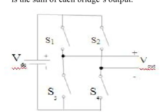
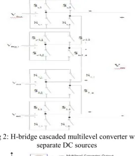
Cascaded H-bridge Converter: A cascaded H-bridge converter is several H-H-bridges in series configuration. A single H-bridge is shown in Figure 1. A single H-bridge is a three-level converter. The four switches S1, S2, S3 and S4 are controlled to generate three discrete outputs Voutwith levels Vdc, 0 and -Vdc . When S1and S4are on, the output is Vdc ; when S2 and S3are on, the output is –Vdc; when either pair S1 and S2 or S3 and S4 are on, the output is 0. An H-bridge cascaded multilevel converter with s separate DC sources is shown in Fig 2. A staircase sinusoidal waveform can be generated by combining specified output levels, which is shown in Figure 3. Load balance control for each H-bridge and each DC source can be acquired by rotating the switching angles to the H-bridges.
The advantages for cascaded multilevel H-bridge converter are the following:
(1) The series structure allows a scalable, modularized circuit layout and packaging due to the identical structure of each H-bridge.
(2) No extra clamping diodes or voltage balancing capacitors is necessary.
(3) Switching redundancy for inner voltage levels is possible because the phase voltage is the sum of each bridge’s output.
Fig 2: H-bridge cascaded multilevel converter with separate DC sources
Fig 3: Staircase sinusoidal waveform generated by H-bridge cascaded multilevel converter
The disadvantage for cascaded multilevel H-bridge converter is the following:
(1) Needs a separate DC source
Another kind of cascaded multilevel converters with transformers using standard three-phase bi-level converters has recently been proposed. The circuit is shown in Figure 4. The converter uses output transformers to add different voltages. In order for the converter output voltages to be added up, the outputs of the three converters need to be synchronized with a separation of 120 degrees between each phase. For example, obtaining a three-level voltage between outputs a and b, the output voltage can be synthesized by Vab = Va1-b1+Vb1-a2+Va2-b2. An isolated transformer is used to provide voltage boost. With three converters synchronized, the voltages Va1-b1, Vb1-a2, Va2-b2, are all in phase; thus, the output level can be tripled.
Fig 4: Cascaded multilevel converter with transformers using standard three-phase bi-level
converters
The advantage for the cascaded multilevel converters with transformers using standard three-phase bi-level converters is the three converters are identical. So control would be simple. The topology has two disadvantages. The first is the three converters need separate DC sources; the second is it needs a transformer to add up the output voltages.
3. PV INTERFACE & MULTILEVEL INVERTER:
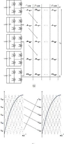
different panels uneven. The multilevel cascade topology does not require any of the H-bridges to be switched in a determined sequence as would be the case for a diode clamped multilevel (DCM) converter. This gives freedom to switch the H-bridges in the circuit in any order, which can be used as strategy to equalize the power transferred from individual panels. The control strategy implemented shifts the carrier signal over N cycles in the case of a (2N+1) level inverter to make it possible to draw the same amount of power from each string. Shifting the carrier down for each cycle is the same as physically changing the position of the H-bridges shown in Fig 7(a) for an 11-level inverter. In that figure five cycles of the fundamental frequency are needed to have each panel switch position with the other four. The energy stored in the capacitor will come to help in this process in a cycle-by-cycle basis to avoid a considerable voltage drop due to its considerable large capacitance (1000 uF).
Fig 6: Control block diagram.
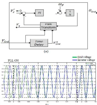
4. SYNCHRONIZATION & TRACKING CONTROL SYSTEM:
Synchronization between inverter and grid means that both will have the same phase angle, frequency and amplitude. This can be done noise proof with respect to the grid by sensing the grid voltage in a Phase Locked Loop (PLL). Typical PLL algorithms include inverse Park-based PLL, Hilbert transformer-based PLL, and transport delay-based PLL. The one to be included in this design is the transport delay-based PLL. Fig 12(a) shows the block diagram of the PLL algorithm. Notice that the delayed angle can be directly controlled at the computer station during the experiment to provide the signal in quadrature with the grid, which is the input to the Park transform block. The PLL output is the actual angle position of the grid voltage. This signal is used to generate the sine wave that is used as the reference signal to the control system, which will generate the SPWM, signals to drive the switches. The time required for synchronization will be dependent on the PI block parameters. Fig 12(b) shows the PLL synchronization simulation. In that figure, the PLL starts its synchronization at 0.03 second, and it is in synchronization after about 0.13 second. Since the
angle is now known, it is possible to control the phase difference between inverter and grid by controlling δ. This allows the power flow to be controlled according to (1).
Where Vinv is the inverter voltage, Vgrid is the grid voltage, XL is the connection impedance, and δ is the angle between grid and inverter.
Instead of sensing the individual panel voltages, the maximum power point tracking (MPPT) algorithm determines the optimal point of operation of the panel by calculating the output power and phase angle variation. It monitors output voltage and current parameters by making small changes on the phase angle and looking at the power variation, as in a hill climbing optimization method to track the maximum power point.
IV. SIMULATION RESULTS:
Fig 8: Input signal parameters
Fig 9: Expected AC output voltage waveform with (a) voltage gradational method and (b) PWM carrier
method.
Fig 10: Simulation results of AC output voltage waveform with (a) voltage gradational method and (b)
PWM carrier method.
Fig 11: Voltage and Current measurement of H-Bridge
III.SIMULATION CIRCUIT
:
Fig 12: Voltage and current measurement of multilevel H-bridge
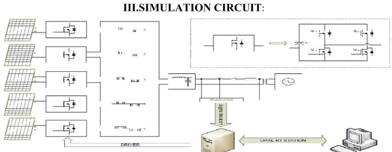
An H-bridge is an electronic circuit which enables a voltage to be applied across a load in either direction. Each one of the five H-bridges has its own 200 W PV panel connected as an independent source. The control signals to the bridges are sent by the OPAL-RT workstation where software and I/O boards are installed. The system acquires grid voltage and inverter output current and voltage to the control block (OPAL-RT workstation) to generate the driver signals to the inverter. The RT-Lab control platform, which connects the software (PWM, PLL, MPPT) with the hardware (solar panel, grid, 11- level cascaded H-bridge inverter), to create a real time platform, is the main tool to perform the experiments. Due to hardware limitation, the maximum achievable frequency for the SPWM signals is 2 kHz which requires bulk filtering components. A 2 kHz discrete-time RT Lab drives the inverter with five solar panels as DC inputs and provides a waveform to interface with the 60 Hz AC grid.
Fig 13: (a) Transport delay-based PLL algorithm and (b) voltage synchronization using PLL
V. CONCLUSION:
This paper presented the design and simulation of 11-level Cascaded H-bridge Grid-tied Inverter for the application of Solar Panels as DC sources to interact with the power grid. A SPWM approach was presented to deal with the uneven power transferring characteristics of the conventional SPWM modulation technique. This technique proved to be successful due to the irradiance profile and the use of capacitors to smooth the voltage fluctuation. The system was driven at 2 kHz because of speed constrains of the control platform, which required bulk filter components.
The grid connection results were shown using the proposed MPPT algorithm. Future work includes the use of a DSP platform to increase switching frequency and reduce filter requirements. The entire PV system structure and its interaction with the grid through PLL and MPPT algorithms are clearly shown by simulation results.
VI. REFERENCES:
[1] J. M. Carrasco, L. G. Franquelo, J. T. Bialasiewicz, E. Galvan, R. C. P. Guisado, Ma. A. M. Prats, J. I. Leon, N. Moreno-Alfonso, “Power-Electronic Systems for the Grid Integration of Renewable Energy Sources: A Survey,” IEEE Transactions on Industrial Electronics, vol. 53, no. 4, pp. 1002-1016, June 2006.
[2] A. J. Morrison, “Global Demand Projections for Renewable Energy Resources,” IEEE Canada Electrical Power Conference, 25-26 Oct. 2007, pp 537-542.
[3] J. Rodriguez, S. Bernet, Bin Wu, J. O. Pontt, S. Kouro, “Multilevel Voltage Source Converter Topologies for Industrial Medium-Voltage Drives, ”IEEE Transactions on Industrial Electronics, vol. 54, no. 6, pp. 2930-2945, Dec. 2007.
[4] L. M. Tolbert, F. Z. Peng, “Multilevel Converters as a Utility Interface for Renewable Energy Systems,” IEEE Power Engineering Society Summer Meeting, Seattle, Washington, July 15-20, 2000, pp. 1271-1274. [5] S. Khomfoi, L. M. Tolbert, “Multilevel Power Converters,” Power Electronics Handbook, 2nd Edition Elsevier, 2007, ISBN 978-0-12-088479-7, Chapter 17, pp. 451-482.
[6] S. Busquets-Monge, J. Rocabert, P. Rodriguez, S. Alepuz, J. Bordonau, “Multilevel Diode-clamped Converter for Photovoltaic Generators with Independent Voltage Control of Each Solar Array,” IEEE Transactions on Industrial Electronics,vol. 55, July 2008, pp. 2713-2723.
Photovoltaic Application,” IEEE Applied Power Electronics Conference and Exposition, Feb. 24-28, 2008, pp. 148-153.
[8] S. A. Khajehoddin, A. Bakhshai, P. Jain, “The Application of the Cascaded Multilevel Converters in Grid Connected Photovoltaic Systems,” IEEE Canada Electrical Power Conference, 25-26 Oct. 2007, pp. 296-301.
[9] S. Ozdemir, E. Ozdemir, L. M. Tolbert, S. Khomfoi, “Elimination of Harmonics in a Five-level Diode-clamped Multilevel Inverter Using Fundamental Modulation,” International Conference on Power Electronics and Drive Systems, Nov. 27-30, 2007, pp. 850-854.
[10] J. S. Lai, F. Z. Peng, “Multilevel Converters - A New Breed of Power Converters,” IEEE Transactions on Industry Applications, vol. 32, no. 3, May/Jun. 1996, pp. 509-517.
[11] B. Kavidha, K. Rajambal, “Transformerless Cascaded Inverter Topology for Photovoltaic Applications,” India International Conference on Power Electronics, Chennai, India, Dec. 19-21, 2006, pp. 328-331.
[12] O. Alonso, P. Sanchis, E. Gubia, L. Marroyo, “Cascaded H-bridge Multilevel Converter for Grid Connected Photovoltaic Generators with Independent Maximum Power Point Tracking of each Solar Array,” IEEE Power Electronics Specialist Conference, 15-19 June 2003, pp. 731-735.
[13] A. Abete, R. Napoli, F. Spertino, “A Simulation Procedure to Predict the Monthly Energy Supplied by Grid Connected PV Systems,” Photovoltaic Energy Conversion, 2003. Proceedings of 3rd World Conference on, vol. 3, 12-16 May 2003, pp. 2427-2430.
[14] E. Villanueva, P. Correa, J. Rodriguez, “Control of a Single Phase H-bridge Multilevel Inverter for Grid-connected PV Applications,” Power Electronics and Motion Control Conference, Poznan, Poland, Sept. 1-3, 2008, pp. 451-455.
[15] R. B. Godoy, H. Z. Maia, F. J. T. Filho, L. G. Junior, J. O. P. Pinto, G. S. Tatibana, “Design and Implementation of a Utility Interactive Converter for Small Distributed Generation,” IEEE Industry Applications Conference, Oct. 8-12, 2006, pp.
[16] S. M. Silva, B. M. Lopes, B. J. C. Filho, R. P. Campana, W. C. Boaventura, “Performance Evaluation of PLL Algorithms for Single-phase Grid-connected Systems,” IEEE Industry Applications Society Annual Meeting, Seattle, Washington, October 3-7, 2004, pp. 2259-2263.
[17] A. Pandey, N. Dasgupta, A. K. Mukerjee, “A Simple Single-sensor MPPT Solution,” IEEE Transactions on Power Electronics, vol. 22, no. 2, March 2007, pp. 698-700.
[18] T. Esram, P. L. Chapman, “Comparison of Photovoltaic Array Maximum Power Point Tracking Techniques,” IEEE Transactions on Energy Conversion, vol. 22, no. 2, June 2007, pp. 439-449.
AUTHOR PROFILE:
1* K RAMA CHAKRAVARTHY I is pursuing M.Tech in Nimra College of Engineering and Technology, Vijayawada. His specialization is Power Electronics. He graduated in Electrical and Electronics Engineering from JNTU Kakinada. His research interest includes Power Electronics and Applications.