Abstract—This paper presents a Model Predictive Control technique applied to a dual active bridge inverter where one of the bridges is floating. The proposed floating bridge topology eliminates the need for isolation transformer in a dual inverter system and therefore reduces the size, weight and losses in the system. To achieve multilevel output voltage waveforms the floating inverter DC link capacitor is charged to the half of the main DC link voltage. A finite-set Model Predictive Control technique is used to control the load current of the converter as well as the floating capacitor voltage. Model predictive control does not require any switching sequence design or complex switching time calculations as used for SVM, thus the technique has some advantages in this application. A detailed analysis of the converter as well as the predictive control strategy is given in this paper. Simulation and experimental results to validate the approach are also presented.
Index Terms—Dual inverter, model Predictive control, open end winding induction motor, floating bridge.
I. INTRODUCTION
HIS paper describes a power converter topology for use with an open-ended three phase load. This converter topology is considered due to its higher fault tolerance capacity, which may be useful in some applications such as EV or HEV applications [1, 2]. The use of a dual inverter bridge allows the converter to emulate the waveforms seen in three-level Neutral Point Clamped (NPC) converters [3]. Recently the dual bridge topology has received attention from researchers due to the simplicity of power stage. The circuit implementation requires fewer capacitors than the flying capacitor topology [4], fewer isolated DC supply than H-bridge converters [5] and fewer diodes than NPC converters [6]. For example, a three-phase three-level NPC converter has 6 extra diodes, the flying capacitor converter requires an additional capacitor control and H-bridge converters require two additional isolated supplies. The other advantages of dual bridge inverter with respect to single ended multi-level inverters includes fault tolerant capability [7] and reduction in the voltage blocking requirement for some of the power semiconductor devices. This topology also maintains the distribution of switching events, leading to a lower device commutation frequency and thus reducing the losses in the system for given output waveform quality. Dual inverter topologies have been considered in numerous papers for different applications.
Manuscript received November 6, 2015; revised January 28, 2016 and March 14, 2016; accepted April 12, 2016.
S. Chowdhury, P. W. Wheeler, C. Patel and C. Gerada are with the Power Electronics Machines and Control Group, Department of Electrical and Electronics Engineering, University of Nottingham, Nottingham NG7 2RD, UK.
(e-mail: [email protected], [email protected], [email protected], [email protected] ).
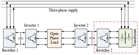
Traditional dual inverter topologies (using two isolated dc sources) have been analyzed [8-10], with different space vector modulation schemes used to generate multilevel output voltage waveforms. A block diagram of a traditional open phase load and associated converters is shown in Fig. 1. It is possible to use a single supply for the dual inverters with common mode elimination technique [8, 11]. These topologies use specific switching combinations that produce equal common mode voltages which cancel at load terminals. Reduction in the number of voltage levels and lower dc bus utilization are the main disadvantages of this type of topology.
[image:1.595.316.540.600.689.2]A modulation technique to balance power between the two inverters in a dual inverter system has been proposed [12, 13]. This topology still uses an isolation transformer; the size of this transformer can be reduced at the expense of reduced modulation index. The floating capacitor bridge topology along with a control scheme to allow the supply of reactive power was introduced in [14]. Other authors [15] have presented methods to compensate for supply voltage droop in order to keep the drive operational in constant power mode. This topology uses a floating capacitor bridge to offset the voltage droop in high speed machines.
To remove the isolation transformer and achieve multilevel output voltage waveforms, a dual inverter with a floating capacitor bridge is considered in this paper. The charging and discharging switching sequences are identified along with the limitation of the available states to allow proper control of the floating capacitor voltage. This paper also presents a model predictive control (MPC) scheme to control the load current and floating dc link voltage independently. MPC consider the model of the system in order to predict the future behavior of the system utilizing all available voltage vectors, thus calculation time will be higher. Identification of the available states limitation will allow the controller to choose between 25 states instead of 64, therefore the calculation time will be lower.
T
ra
ns
fo
rm
er
Three phase supply
Rectifier 1
Inverter 1 Inverter 2
Rectifier 2 Open
Phase Load
Fig. 1. Conventional Dual Active Bridge Topology.
II. PROPOSED DUAL INVERTER SYSTEM
A. Floating capacitor bridge inverter
The floating bridge capacitor dual inverter based topology has previously been analyzed for different applications [14-16]. The circuit can be used to supply
Model Predictive Control for a Dual Active
Bridge Inverter with a Floating Bridge
Shajjad Chowdhury,
Student Member, IEEE
, Patrick W. Wheeler,
Senior Member, IEEE
, Chris
Gerada,
Member, IEEE
and Chintan Patel,
Member, IEEE
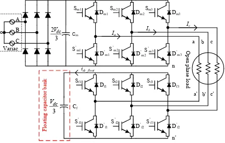
reactive power to a machine and to compensate for any supply voltage droop. In both cases the possibility of multilevel output voltage waveforms were not considered. A control scheme to charge the floating capacitor bridge along with multilevel voltage output has been presented [17]. In this reported method the main converter works in six step mode and the floating converter is called conditioning inverter which is improving the waveform quality. In this paper the capacitor in the floating inverter bridge is charged using redundant switching combinations to remove the need for any isolation transformer and to achieve multilevel output voltage waveforms. Fig. 2 shows a block diagram of the dual inverter with a floating bridge and associated capacitor. The use of a dc link voltage ratio of 2:1 allows the dual bridge inverter to produce up to a four-level output voltage waveform [18]. A circuit diagram of proposed system is presented in Fig 3.
Three phase supply
Rectifier 1
Inverter 1 Inverter 2
C
ap
ac
ito
r
ba
nk
[image:2.595.315.536.201.419.2]Open Phase Load
Fig. 2. Block diagram of proposed floating bridge topology.
B. Principles of operation
The floating bridge capacitor voltage can be controlled by directing the load current through the floating capacitor in either direction. To consider the direction of the load current through the floating capacitor, switching combinations produced by the dual two-level inverter have been analyzed. The dual two-level inverter produces 64 switching states as shown in fig. 4, which is a representation of three phase quantity utilizing a single vector in the α-β co-ordinates. The space vector diagram is obtained considering that both the converters are fed by isolated voltage sources with a voltage ratio of 2:1.
O
pe
n p
ha
se
lo
ad
Sm1 Sm2 Sm3
Sf1 Sf2 Sf3
a b c
F
lo
at
in
g
ca
pa
ci
to
r
ba
nk
Ia
Ib
Ic
S’
m1 S’m2 S’
m3
S’
f1 S’f2 S’f3
Dm1
D’
m1 D’m2 D’m3
Dm2 Dm3
Df1 Df2 Df3
D’
f1 D’f2 D’f2
A B C
Cf
Cm
o
Variac
a' b' c' n
n' 3
2Vdc
3 dc V
[image:2.595.55.279.244.359.2]idc_float
Fig. 3. Circuit diagram of proposed floating bridge topology (Capacitor bank is charged to half of the main DC link voltage).
In the state diagram red numbered switching combinations discharge the floating capacitor, while the green numbered switching combinations charge the floating capacitor. The blue numbered switching combinations hold the last state of capacitor and are therefore neutral in terms of the state of charge of the floating capacitor [19, 20]. As an example state (74) in Fig.4 gives the switching sequences for
both converter’s top switches 7 (1 1 1) represents the top three switches for main inverter and 4(0 1 1) represents the switching states for top three switches of the floating converter. A circuit diagram of charging and discharging switching states are presented in Fig. 5. It can be seen from the Fig. 5 that combination (11) charges the floating capacitor by directing the current from the positive to negative terminal of the floating capacitor. Combination (74) will result in a current in the opposite direction and will therefore act to discharge the capacitor whilst giving the same output voltage. Combinations ending with 7 (111) or 8 (000) are zero states and will therefore have no impact of floating capacitor's voltage.
25
24
15
14
13
64
63 62 53 52
51 42 41
46 31
36 35 26
37 38 21 34 27 28
32 45 33 86 22 85 23 16
47 48 44
81
71 78
77 88
11
74
84 17 18
56 43 55 82
72
66
83
73 12 65
57 58 61 54 67 68
87
Vdc
Vdc/3
2Vdc/3
Vdc = (Vdc/3)+(2Vdc/3)
ref
V
[image:2.595.320.535.452.563.2]
Fig. 4. Space vector of dual two-level inverter (source ratio 2:1).
1 0 0 1 0 0
Sm3 Sm2 Sm1
S’ m3 S’
m2 S’
m1
Sf1 Sf2 Sf3
S’
f1 S’f2 S’f3 (11)
2V
dc
/3
cf +
-1 -1 -1 (74) 0 1 1
cf + -Sm3
Sm2 Sm1
S’ m3 S’
m2 S’
m1
Sf1 Sf2 Sf3
S’
f1 S’f2 S’f3 Vdc
/3
2V
dc
/3
Vdc
/3
Fig. 5. Current flow for different switching states.
From Fig. 4 it is evident that if the reference voltage resides in outer hexagon then there are only two switching combinations in each sector to charge the floating capacitor. This is insufficient to maintain the charge under all operating conditions; therefore a restriction has to be imposed. As a result the achievable number of voltage levels is reduced to three along with lower than ideal DC bus utilization. Therefore the floating capacitor can charge to half of the main DC link capacitor voltage only if the reference voltage resides inside the green hexagon [Fig. 4].
III. PREDICTIVE CONTROL
A. Control Procedure
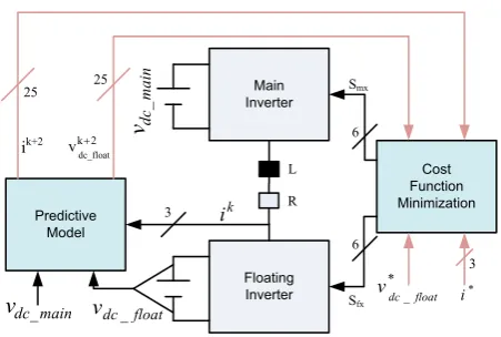
[image:2.595.57.280.527.669.2]achieve accurate control good quality load and converter modeling is necessary. Predictive control uses the finite number of possible switching states generated by the converter and in this case evaluates the load current and floating capacitor voltage for each state. The predicted value is then compared to reference value at each sample time and the control selects the next switching states to minimize the predicted error. A block diagram of control strategy for the proposed system with an R-L load is shown in Fig. 6 and the control algorithm can be summarized as
The values of current and floating DC link voltage reference are defined and the actual values are measured.
For each valid switching state of the converter the load current and floating DC link voltage for the next sampling instant are predicted.
A cost function is used to evaluate the error between references and the predicted values for each switching state.
A weighting factor is applied to the floating capacitor voltage term in the cost function to match the error magnitude with current error reference. The switching state that generates the minimum
cost function value is selected and applied to the converter for the next sampling period.
B. Modeling of the converter and load for predictive control
For the proposed converter topology shown in Fig.3, each of the two-level converters has eight possible switching states and when they are connected as shown the total number of states increases to sixty-four. All sixty-four states are presented in the vector diagram shown in Fig. 4. It can be seen that there are a lot of redundant states which can be ignored to make the calculation time smaller. To charge the capacitor and to achieve three-level voltage output only twenty-five states are selected. All the vectors of the outer hexagon are ignored.
The converter state combinations are selected so that the average generated voltages across the load are 180° phase shifted from each other. This phase shift is necessary to achieve maximum available converter voltage across load terminal. Using Clarke’s transformation the balanced three phase system can be represented as two phase (α-β) system using equation (1). In the equation X represents either the current or the voltage, as appropriate.
b c
c b a X X X X X X X 3 1 2 3 1 (1)
The output voltage of the converters can therefore be synthesized as a function of DC link voltage and the state of the switching devices Sα and Sβ.
main dc m main main dc m main
V
S
V
V
S
V
_ _ _ _ _ _
(2) float dc f float float dc f floatV
S
V
V
S
V
_ _ _ _ _ _
(3) float main float main V V V V V V _ _ _ _ (4)Subscript a, b, c represents the three phase system, α-β
represents the two phase system after using Clarke’s transformation. Components of main inverter and floating inverters are denoted by subscript ‘main’ and ‘float’. Now the continuous model of the load can be modeled in α-β
coordinates using equations (5 - 8).
dt di L Ri
V (5)
The equation (5) is then used to get the predicted current value L Ri L V dt
di
(6) L Ri L V Ts i
ik k k k
1 (7) k k k V L Ts i L RTs
i
1 1 (8)
Here, R and L are the load resistance and inductance, ik and Vk are the load current and voltage at current sample
time in α-β coordinates. Ts is the sample time and ik1 is one sample ahead predicted current value. To control the capacitor voltage the charging and discharging switching combinations are identified the green and red switching sequences in Fig. 4 respectively. Then DC link current for the floating DC link is identified.
i
S
i
S
i
dc_float
_float
_float (9)The prediction for floating capacitor voltage can be found by evaluating:
dt
dv
C
i
dc_float
dc_float (10)k float dc k k float dc
v
C
i
Ts
v
dc float_ 1 _ _
*
(11)Here,
i
dc_float is the floating DC link current, C is the1 1
2 1
k k
k V L Ts i L RTs
i (12)
1 _ 1 2 _ _ *
k
float dc k
k float
dc C v
i Ts
v dc float
(13)
Here, (k+2) refers to the predicted value at two sample periods ahead. As the DC link voltage does not change considerably in one sample period thus, 1
_ k
float dc
v is
assumed to be the current floating DC link value in this paper. The reference α-β currents are generated as sine and cosine functions which are 90o phase shifted from each
other. The reference floating DC link voltage is calculated from main inverters DC link voltage magnitude; by simply dividing the main inverters DC link voltage amplitude by two. To achieve proper control over the floating capacitor voltage a table is created to identify the floating inverters DC link current along with its direction related to the switching states. Identification of the floating DC link current is achieved using the states shown in Fig.5. The floating DC link voltage is then predicted using these current values and then compared with the reference value. The control is included in the cost function to minimize the error at the end of the next sampling period.
To predict the reference current value two sample periods ahead a Lagrange extrapolation method is used [22]. The reference current value becomes:
2 1
2 * * *
*k 6i k8i k 3i k
i (14)
(k+2) is two step ahead predicted value, k is the current value, (k-1) is the previous value and (k-2) is two step behind value. The reference for the floating DC link voltage is generally constant at all times. The two cost functions are defined separately for the current and voltage, all the values used in these calculations are two sample periods ahead of the sample time.
* 2
2
* 2
22
2
k k
i i i i i
g k k
(15)
2
2_ *
_
_float dc float dck float
v V v
g
(16)float v
i
g
g
g
_ (17)Here, * _ * float dc v i
(18)Here g is the total cost function and λ is the weighted factor to normalize the floating voltage error in contrast with the current errors.
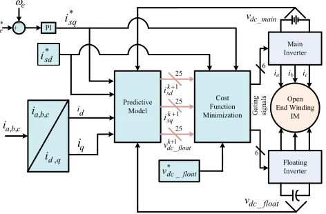
Finally, to demonstrate the performance of the converter an open end winding induction motor is used as a load. The predictive control algorithm used in this paper is based on well-known Indirect Rotor Flux Oriented (IRFO) induction motor control [23].The speed loop of the IRFO control will generate the torque producing current reference (i*
sq) and the
field current (i*sd) reference will be a constant value. Rotor
flux oriented stator voltage d-q equations (19 and 20) are used [23] to predict the d-q axis current shown in equations (21) and (22).
Floating Inverter Main Inverter Predictive Model Cost Function Minimization R L k i 3 float dc v _ main dc v _ mai n dc v _ * _float dc
v i*
3 6 6 Smx Sfx 25 25
ik+2 k2
[image:4.595.315.541.53.205.2]dc_float v
Fig. 6. Predictive current control of dual two-level inverter with one bridge floating with a R-L load.
To achieve two steps ahead current values first, one step ahead current values are calculated using previously applied voltage vector along with present current values. These one step ahead current value is then used to calculate the two step ahead current values using all available voltage vectors to minimize the predicted errors.
rd dt d r Lm L qs i e sd i dt d s L sd i s R sd
V
* (19) rd r L m L e ds i e sq i dt d s L sq i s R sq
V
* (20)
2 1 1 k 1
sq e s k sd s sd s k sd k sd i L i R V T i i (21) s r k sd m e k sd e s k sq s sq s k sq k
sq L L
i L i L i R V T i i 1 2 1 1 1
2 (22)
Here, * sd
V and Vsq* are the reference d and q axis stator
voltages, Rs, Ls, Lr and Lm are the stator resistance, stator
inductance, rotor inductance and magnetizing inductance respectively. Terms isd, isq, ωeandψrd are the stator d and q
axis currents, electrical speed and rotor d-axis flux correspondingly.Here, sigma (σ) is the leakage factor of the machine and can be described using equation (23).
Lm2 LsLr
1
(23)
As the controller is in d-q plane the converter voltages and currents can be transferred to d-q plane, using equation (24).
r
rq r r d X X X X X X sin cos sin cos (24)
re r sd sq r i i * * (25) r rr RL
(26)
Here, subscript d,q and θψr represents the d-q axis components and rotor flux angle. If the machine is operating in constant flux region then the rotor flux angle can be calculated using equation (25). In equation (25), re
time constant which can be described as equation (26) and superscript ‘*’ denotes the reference values. The floating DC link capacitor voltage is predicted using equation (13). The controller will generate different q-axis current reference for different operating conditions of the machine. To normalize the errors all three cost functions will require three separate weighing factors. The cost functions with different weighting factors are presented in equation (27 - 29).
* 2
2
* 2
22
2
k
sq sq q k sd sd d
i i i i i
g k k (27)
2
2_ *
_
_float dc dc float dck float
v V v
g
(28)float v
i g
g
g _ (29)
Here, λd, λq and λdc are the weighting factor for d-q axis
current and floating DC link voltage. The weighting factors are calculated using reference values, the stator d-axis reference current and floating capacitor voltage references are kept constant. The only variable is the reference torque producing (q-axis) current, which varies depending on loading conditions. To provide equal weight to all these three controllers the error of control variables is normalized using equation (30). The normalizing factor will update automatically depending on the load. The calculation of the weighting factors are provided in equation (30).
c b a i,,
q d i , Predictive Model d i * sd i q i * sq i G at in g si gn al s c b a i,,
+_ * e e PI Main Inverter Floating Inverter Open End Winding IM 6 6 Cost Function Minimization 25 25 25 1 k sd i 1 k sq i 1 _ k float dc v main dc v _ float dc v _ * _float dc v
[image:5.595.308.547.362.495.2]ia ib ic
Fig. 7. Block diaram of inducton motor drive using predictive current control of dual two-level inverter with one bridge floating.
*
_ * * _ * * * * * * _ * * _ * * * * _ * * _ * * _ * * * * _ * float dc q float dc d q d d q dc float dc q float dc d q d float dc d q float dc q float dc d q d float dc q d V i V i i i i i V i V i i i V i V i V i i i V i (30)A simplified block diagram of a motor drive using predictive control algorithm to control the d-q axis current is shown in Fig. 7. This is a hybrid control where fast inner current control loops are replaced with predictive control algorithm. The control requires the additional PI controller to generate the reference torque producing current. The floating DC link voltage reference is set using a constant
value which is equal to half of the main inverters DC link voltage to reduce calculation time for drive operation. C. Simulation results
The proposed system has been simulated using both PLECS and SIMULINK to compare losses between three different converter topologies. After the losses are compared, the converter performance with predictive control algorithm is demonstrated for static R-L load and with an induction machine.
[image:5.595.54.290.370.525.2]Three converter types were selected to compare losses of the proposed power converter topology, a single sided three-level NPC, a dual two-three-level inverter with equal DC link voltage ratio and the proposed dual inverter topology. All these three topologies provide three-level output voltages and therefore it is important to compare them in terms of losses. To calculate the losses the NPC and the main converter of the floating dual inverter was supplied with 970 volts DC and the secondary of floating topology was charged to 485 Volts. Dual inverter with equal DC link voltage was supplied with 485 volts DC on both sides. These DC link voltage levels were selected to achieve the rated fundamental load voltage of 690 Volts RMS. The dead-time was set to
4
.
1
s
. The device losses were calculated using semiconductor device characteristics selected according to required blocking voltage and current requirements of the topology.Fig. 8. Loss comparison in different power converter topologies.
Fig. 9. Phase voltage (VAA’) and current (Ia) when the reference is set to 4
[image:6.595.314.544.120.261.2]Amps.
[image:6.595.52.284.244.522.2]Fig. 10.FFT of phase current.
Fig. 11.Phase voltage (VAA’) and current (Ia) when the refernce is set to 9
[image:6.595.308.546.306.704.2]Amps.
Fig. 12.FFT of phase current.
Snubbers and parasitic inductors were ignored in this simulation. The output pulses were slightly altered to eliminate the dead-time interval effect inherent in this family of converter topologies [24]. Fig. 9 shows the phase voltage and current when the system demands peak current of 4 Amps. This result shows the two-level operation of the converter and the phase current follows the reference value with a small error as expected. Fig. 11 shows the same results for a reference of 9Amps, and show operation with a
three-level output voltage waveform. It can be seen that the actual current is closely following the reference current and that the converter can achieve a multilevel voltage output waveform. Frequency spectrums of both the currents are presented in Fig. 10 and Fig. 12, in both cases harmonics are spread all over the frequency range.
Fig. 13.Step response of the controller from top to bottom: Floating DC link voltage and three phase currents.
Fig. 14.Controller response to a step load applied after speed reaches steadystate. Top to bottom: floating capacitor voltage, rotor speed, d-axis current, q-axis current and electromagnetic torque.
[image:6.595.52.284.557.653.2]from the Fig. 13 that the output current magnitude changes immediately according to the change in reference and there is no effect on the floating capacitor voltage.
Finally, an open end winding induction motor was used to verify the performance of the converter. To achieve the results the main converter was supplied by a 500 Volts DC source and the floating capacitor voltage was charged at 250 Volts. The sampling frequency was set to 12.5 kHz. The performance of the drive is presented in Fig. 14. In the figure the machine is in steady state at 700 rpm when a step load is applied to the machine at t = 0.8 seconds and back to zero at t=1.1 seconds. The torque producing q-axis current quickly increases to counter the load torque. It can be seen from the simulation results in Fig. 13 and in Fig.14 that at no time does the capacitor voltage overcharge or collapse.
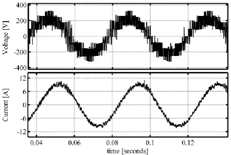
[image:7.595.56.280.265.399.2]The phase voltage and current are shown in Fig. 15 for the operation when the machine was loaded along with the frequency spectrum of the phase current shown in Fig.16.
[image:7.595.313.540.288.668.2]Fig. 15.Phase voltage (Vaa’) and current (Ia) when the machine is loaded.
Fig. 16.FFT of phase current.
It can be conclude from the simulation results that the proposed system can maintain the capacitor charge under all operating conditions and achieve multilevel output voltage waveform.
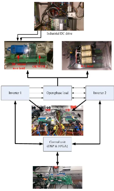
D. Experimental results
To validate simulation results an experimental converter has been built and tested, as shown in Fig. 17. The power converters used for this experiment is one of the ‘off the shelf’ converters manufactured by SEMIKEON [27]. These two-level converters have R-C snubbers and input and output common mode inductors. The converter also has onboard defined dead-time that varies from 4 – 4.1 μs along with propagation delay which varies from 0.1 to 0.2 μs and thus becomes very difficult to align the pulses for dead-time voltage spike removal algorithm. The power circuit of the experimental converter is shown in Fig.18. The system has been tested with an R-L load and the parameters are shown in table I. To demonstrate the behavior of the dual inverter system with predictive control, a demand reference current of 4Amps sinusoidal reference with a 50 Hz frequency was applied. The results are shown in Fig. 19 and can be
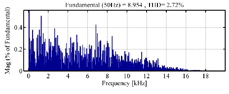
compared to the simulation results in Fig 9. Fig. 20 shows the frequency spectrum of phase current and it can be seen that the harmonic distortion is high and the harmonics are spread over the frequency range, as expected from model predictive control due to the inherent variable switching frequency. To demonstrate the multilevel operation of the converter, a 50 Hz and 9Amps current reference was applied to the control system. The results are presented in Fig.21. In the figure the converter achieves multilevel voltage output waveform as expected. Fig. 22 shows the frequency spectrum of the phase current waveform for multilevel voltage output. The current distortion is reduced from 8.66% to 4.05%. One way to control the frequency spectrum is to use modulated model predictive control [25, 26], but this is beyond the scope of this paper. A step change in current reference from 4Amps to 9Amps was demanded from the system to check the transient behavior of the control scheme. Results are presented in Fig. 23. It can be seen that the load current tracks the change in reference and it has no impact on floating capacitor voltage.
Fig. 17.Experimental Converter and Contorl Platform.
[image:7.595.53.283.428.515.2]winding induction motor drive, the main converter was supplied by a 500 Volt DC source. The floating capacitor was initially charged using reference d-axis current. After the floating capacitor was charged to the required value a speed command was set at 700 rpm. The results presented show the steady state and dynamic performance of the motor drive. It can be seen form Fig. 25 that, at steady state no load operation the floating capacitor voltage fluctuates but it is less than 3% of the steady-state value. A step load was applied at t = 1.45 seconds, reference q-axis current steps up immediately to counter the load torque. It can be seen that the floating DC link voltage is more stable when the machine is loaded, this is because the machine is drawing real power and the capacitor voltage can be charged and discharged quickly. It can be seen from Fig. 23 and Fig. 25 that the controller is robust enough to maintain the floating DC link voltage and currents to the required value for both static R-L load and induction motor drive. The phase voltage and current for the machine are presented in Fig. 26. It can be seen that the converter achieves multilevel output voltage.
S3 S2
S1
S6 S5
S4
Common mode choke
RC snubber
RC snubber Y-capacitor
+
- Common
mode choke
D
C
li
nk
c
ap
ac
it
or D
1 D2 D3
[image:8.595.313.543.49.211.2]D4 D5 D6
[image:8.595.312.543.248.524.2]Fig. 18.SEMIKRON’s SKAI module.
Fig. 19.Current reference is set to 4 amps. Top to bottom : phase voltage VAA’, and phase current Ia.
Fig. 20.FFT of the phase current.
Fig. 21.Current reference is set to 9 amps. Top to bottom : phase voltage VAA’, and phase current Ia.
[image:8.595.52.284.275.637.2]Fig. 22.FFT of phase current.
Fig. 23.A step change in current reference from 4 to 9 amps. Top to bottom : floating capacitor voltage and three phase currents.
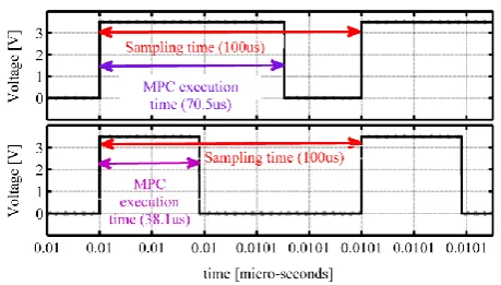
Fig. 24.MPC exicution time for utilizing 64 states (top), utilizing 25 states (bottom) for R-L load operation.
[image:8.595.314.544.562.692.2] [image:8.595.52.285.672.762.2]Furthermore, the snubber circuits are absent in simulation. The snubber circuits present in the experimental rig forms an L-C resonant circuit and cause oscillation in the current waveform thus increases the current harmonic distortion in experimental results.
[image:9.595.316.542.48.199.2]Fig. 25.Controller response to a step load applied after speed reaches steadystate. Top to bottom: floating capacitor voltage, rotor speed, d-axis current, q-axis current and electromagnetic torque.
TABLE I. PARAMETERS
R-L Load
Resistance R 10.6 Ohm
Inductance L 3.8e-3 H
DC link capacitance C 3250 μf
Main DC link Vdc_main 200 Volts
Floating DC link Vdc_float 100 Volts
Sampling frequency fs 20 kHz
Switching frequency (average) fsw 4 kHz Induction motor
Stator resistance Rs 1.4 Ohm
Rotor resistance Rr 1.02 Ohm
Stator leakage inductance Lls 0.01151 H
Rotor leakage inductance Llr 0.00926 H
Magnetizing inductance Lm 0.22580 H
DC link capacitance C 3250 μf
Main DC link Vdc_main 500 Volts
Floating DC link Vdc_float 250 Volts
Sampling frequency fs 12.5 kHz
Switching frequency (average) fsw 3 kHz
[image:9.595.51.288.112.497.2]Fig. 26.Phase voltage (Vaa’) and current (Ia) when the machine is loaded.
Fig. 27.FFT of the phase voltage.
Fig. 28.FFT of the phase current.
IV. CONCLUSIONS
A dual active bridge converter with a floating inverter has been proposed and analyzed in this paper. A set of charging and discharging switching sequences have been identified to enable the control of the floating capacitor bridge voltage to half of the main DC link voltage. This particular ratio is used to achieve multilevel output voltage waveforms. A model predictive control scheme is used to control the load current and floating capacitor voltage. The proposed system has been simulated and an experimental setup has been used to validate the results. It has been shown that the proposed system can charge the capacitor to the required value under all operating conditions and that the converter can achieve multilevel output voltage waveforms.
V. REFERENCES
[1] F. Meinguet, N. Ngac-Ky, P. Sandulescu, X. Kestelyn, and E. Semail, "Fault-tolerant operation of an open-end winding five-phase PMSM drive with inverter faults," IEEE Conf. on Ind. Electron. Soc.
IECON, pp. 5191-5196, 2013.
[2] B. A. Welchko, T. A. Lipo, T. M. Jahns, and S. E. Schulz, "Fault tolerant three-phase AC motor drive topologies: a comparison of features, cost, and limitations," IEEE Trans. Power Electron., vol. 19, pp. 1108-1116, 2004.
[3] K. Sivakumar, A. Das, R. Ramchand, C. Patel, and K. Gopakumar, "A three level voltage space vector generation for open end winding IM using single voltage source driven dual two-level inverter," IEEE
[image:9.595.309.542.231.408.2] [image:9.595.47.296.550.778.2][4] D. Janik, T. Kosan, P. Kamenicky, and Z. Peroutka, "Universal precharging method for dc-link and flying capacitors of four-level Flying Capacitor Converter," IEEE Conf. on Ind. Electron. Soc.
IECON, pp. 6322-6327, 2013.
[5] O. A. Taha and M. Pacas, "Hardware implementation of balance control for three-phase grid connection 5-level Cascaded H-Bridge converter using DSP," IEEE Int. Symp. Ind. Electron. ISIE, pp. 1366-1371, 2014.
[6] W. Bingsen, "Four-level neutral point clamped converter with reduced switch count," IEEE Power Electron. Spec. Conf. PESC, pp. 2626-2632, 2008.
[7] B. A. Welchko and J. M. Nagashima, "A comparative evaluation of motor drive topologies for low-voltage, high-power EV/HEV propulsion systems," IEEE Int. Symp. Ind. Electron. ISIE, pp. 379-384 vol. 1, 2003.
[8] N. Bodo, M. Jones, and E. Levi, "PWM techniques for an open-end winding fivephase drive with a single DC source supply," IEEE
Conf. on Ind. Electron. Soc. IECON, pp. 3641-3646, 2012.
[9] K. Ramachandrasekhar, S. Mohan, and S. Srinivas, "An improved PWM for a dual two-level inverter fed open-end winding induction motor drive," Int. Conf. on Electrical Machines ICEM, pp. 1-6, 2010.
[10] Y. Zhao and T. A. Lipo, "Space vector PWM control of dual three-phase induction machine using vector space decomposition," IEEE
Trans. Industry App., vol. 31,pp. 1100-1109, 1995.
[11] M. R. Baiju, K. K. Mohapatra, R. S. Kanchan, and K. Gopakumar, "A dual two-level inverter scheme with common mode voltage elimination for an induction motor drive," IEEE Trans. Power Electron., vol. 19, pp. 794-805, 2004.
[12] G. Grandi and D. Ostojic, "Dual inverter space vector modulation with power balancing capability," IEEEEUROCON, pp. 721-728, 2009.
[13] D. Casadei, G. Grandi, A. Lega, and C. Rossi, "Multilevel Operation and Input Power Balancing for a Dual Two-Level Inverter with Insulated DC Sources," IEEE Trans. Industry App., vol. 44, pp. 1815-1824, 2008.
[14] K. Junha, J. Jinhwan, and N. Kwanghee, "Dual-inverter control strategy for high-speed operation of EV induction motors," IEEE Trans. Ind. Electron., vol. 51, pp. 312-320, 2004.
[15] R. U. Haque, A. Kowal, J. Ewanchuk, A. Knight, and J. Salmon, "PWM control of a dual inverter drive using an open-ended winding induction motor," IEEEApplied Power Electron. Conf. and Expo. APEC, pp. 150-156, 2013.
[16] J. Ewanchuk, J. Salmon, and C. Chapelsky, "A Method for Supply Voltage Boosting in an Open-Ended Induction Machine Using a Dual Inverter System With a Floating Capacitor Bridge," IEEE
Trans. Power Electron., vol. 28, pp. 1348-1357, 2013.
[17] K. A. Corzine, M. W. Wielebski, F. Z. Peng, and W. Jin, "Control of cascaded multilevel inverters," IEEE Trans. Power Electron., vol. 19, pp. 732-738, 2004.
[18] B. V. Reddy and V. T. Somasekhar, "A Dual Inverter Fed Four-Level Open-End Winding Induction Motor Drive With a Nested Rectifier-Inverter," IEEE Trans. Ind. Info., vol. 9, pp. 938-946, 2013.
[19] S. Chowdhury, P. Wheeler, C. Gerada, and S. Lopez Arevalo, "A dual inverter for an open end winding induction motor drive without an isolation transformer," IEEEApplied Power Electron. Conf. and
Expo. APEC, 2015 IEEE, 2015, pp. 283-289.
[20] S. Chowdhury, P. Wheeler, C. Gerada, and C. Patel, "A dual two-level inverter with a single source for open end winding induction motor drive application," Euro. Conf. on Power Electron. and App.
EPE-ECCE-Europe, pp. 1-9, 2015.
[21] L. Tarisciotti, P. Zanchetta, A. Watson, S. Bifaretti, and J. C. Clare, "Modulated Model Predictive Control for a Seven-Level Cascaded H-Bridge Back-to-Back Converter," IEEE Trans. Ind. Electron., vol. 61, pp. 5375-5383, 2014.
[22] M. Odavic, P. Zanchetta, M. Sumner, and Z. Jakopovic, "High Performance Predictive Current Control for Active Shunt Filters,"Int. Conf. in Power Electron. and Motion Cont. Conf.
EPE-PEMC, pp. 1677-1681, 2006.
[23] B.K.Bose, "Modern power electronics and AC drives," Prentice
Hall PTR, Upper saddle river, NJ 07458, 2002.
[24] M. Darijevic, M. Jones, and E. Levi, "An Open-end Winding Four-level Five-phase Drive," IEEE Trans. Ind. Electron., vol. PP, pp. 1-1, 2015.
[25] M. Rivera, M. Perez, C. Baier, J. Munoz, V. Yaramasu, B. Wu, et al., "Predictive Current Control with fixed switching frequency for an NPC converter," EEE Int. Symp. Ind. Electron. ISIE, pp. 1034-1039, 2015.
[26] M. Rivera, F. Morales, C. Baier, J. Munoz, L. Tarisciotti, P. Zanchetta, et al., "A modulated model predictive control scheme for a two-level voltage source inverter," IEEE Int. Conf. in Ind. Tech. ICIT, pp. 2224-2229, 2015.
[27] SKAI 45 A2 GD12-WDI Available at: "http://www.semikron.com/products/product/classes/systems/detail/s
kai-45-a2-gd12-wdi-14282032.html" Accessed in: 29th October
2015.
Shajjad Chowdhury (S’15) received BSc degree in Electrical and Electronics Engineering, from The American International University – Bangladesh, in 2009 and MSc degree in Power and Control Engineering, from The Liverpool John Moores University, UK in 2011. In October 2012 he joined Power Electronics, Machines and Control Group at The University of Nottingham, UK, as a PhD student. He is a recipent of Dean of Engineering Research Scholarship for International Excellence for his PhD studies. His research interests include multilevel converters, modulation schemes and high performance AC drives.
Prof Pat Wheeler (M’00-SM’12) received his BEng [Hons] degree in 1990 from the University of Bristol, UK. He received his PhD degree in Electrical Engineering for his work on Matrix Converters from the University of Bristol, UK in 1994. In 1993 he moved to the University of Nottingham and worked as a research assistant in the Department of Electrical and Electronic Engineering. In 1996 he became a Lecturer in the Power Electronics, Machines and Control Group at the University of Nottingham, UK. Since January 2008 he has been a Full Professor in the same research group. He is currently Head of the Department of Electrical and Electronic Engineering at the University of Nottingham. He is an IEEE PELs ‘Member at Large’ and an IEEE PELs Distinguished Lecturer. He has published 400 academic publications in leading international conferences and journals.
Chris Gerada (M’05) received the Ph.D. degree in numerical modeling of electrical machines from The University of Nottingham, Nottingham, U.K., in 2005. He subsequently worked as a Researcher with The University of Nottingham on high-performance electrical drives and on the design and modeling of electromagnetic actuators for aerospace applications. Since 2006, he has been the Project Manager of the GE Aviation Strategic Partnership. In 2008, he was appointed as a Lecturer in electrical machines; in 2011, as an Associate Professor; and in 2013, as a Professor at The University of Nottingham. His main research interests include the design and modeling of high-performance electric drives and machines. Prof. Gerada serves as an Associate Editor for the IEEE TRANSACTIONS ON INDUSTRY APPLICATIONS and is the Chair of the IEEE IES Electrical Machines Committee.