44
Electrical Properties Of Nb-Doped TiO
2Thin Films Deposited
By Co-sputtering Process
Hoang Ngoc Lam Huong
*, Nguyen Minh Hieu,
Nguyen Thi Tien, Nguyen Tran Thuat, Nguyen Hoang Luong
Faculty of Physics, VNU University of Science, 334 Nguyen Trai, Hanoi, Vietnam
Received 12 March 2017
Revised 20 April 2017; Accepted 15 September 2017
Abstract: Nb-doped TiO2 thin films were fabricated by co-sputtering of TiO2 doped 6%wt by
Nb2O5and Nb targets. The anatase polycrystalline thin films were obtained by post-annealing at
350oC in vacuum atmosphere. The electrical properties of the film were determined by the Hall method using standard clove-leaf geometry. The results indicated that: when the Nb concentration increases followed by the numbers of electrons increase from 4×1018 cm-3 to 2.4×1020 cm-3. Meanwhile the resistivity fall down from 10 to 3.5×10⁻³ Ωcm. It means that this co-sputtering process is good method to improve conducting properties of Nb:TiO2 thin film. With low
resistivity and high optical transmittance (higher than 80% in the visible range), the fabricated thin film can be applicable for transparent conducting electrodes.
Keywords: Nb-doped TiO2, TNO thin film, co-sputtering method, transparent conducting.
1. Introduction
Transparent conducting oxides (TCOs) are among the key materials supporting optoelectronics technology [1], and sputter-deposited Sn-doped In2O3 (ITO) has been widely used as a practical TCO material because of its excellent resistivity ρ (~2 × 10⁻⁴Ωcm) and transparency in the visible region [2]. However, rapid growth of new optoelectronic devices, including blue light-emitting diodes, vertical cavity surface emitting lasers (VCSEL) and solar cells, requires the development of new TCOs with unique properties that conventional TCOs do not possess, such as high work function and durability against atomic hydrogen [3]. In addition, effort for the development of new and improved TCOs also arises from technological and global societal demands. Increasing world energy consumption cause the rising of global atmospheric CO2 level which is a major cause of global warming. TCOs are key elements in a number of “green” technologies, such as low-e and solar control windows, photovoltaics, OLEDs for indoor lighting and vehicle heat treatment [4]. This provides further motivation to new TCOs for less environmental impact, lower cost, efficiency improvements in important devices.
_______
Corresponding author. Tel.: 84-1222400966. Email: [email protected]
Recently, Nb-doped anatase TiO2 (Ti1-xNbxO2; NTO) thin films in both epitaxial and polycrystalline forms were found to exhibit low ρ of the order of 10-4 Ωcm and high transmittance of 60 ~ 90 % in the visible region [5-9]. TiO2 has properties that other conventional host materials of TCOs do not possess, such as a high refractive index [10], high transmittance in the infrared region, large static permittivity [11] and high chemical stability especially in a reducing atmosphere [12]
.
These lead us to expect that TNO shave sufficient potential as a next-generation TCOs. As a TCOs, NTO has low infrared transparency, hence possibly becomes a promising material for application of heat-resistant glass window which is an energy saving solution [3].In order to obtain highly conductive NTO films, it is important to encourage oxygen vacancy formation [13]. Thus, crystallization of amorphous films by annealing in reductive atmosphere [14] or using lower-oxide based such as Ti2O3- or Ti-metal based targets [15] are effective methods to prepare highly conducting NTO films. Oxygen-deficient NTO showed metallic conductivity [16]. In this paper, we introduce a reductive deposition process of NTO thin films by co-sputtering of TiO2 doped 6%wt by Nb2O5 and Nb targets in order to obtain highly conductive NTO thin films for application of saving-energy window glass.
2. Experiments
NTO thin films were fabricated on unheated Corning glass substrates. As a target, we used a 2-in. ceramic disk of 6 wt% Nb-doped TiO2 composition and 2-in. metal disk of Nb. The base pressure for each deposition was kept about 310-6 Torr. The total pressure during sputtering process varied from 7.5 to 25 mTorr. The RF sputtering power applied to the ceramic target was kept constant at 90 W during 120 min-process, while DC sputtering power applied to the metal target was kept at 20W. Polycrystalline NTO films were obtained by annealing as-deposited thin film at 350oC in vacuum (~110-5 Torr) or N2 atmosphere within 30 min.
The thickness of NTO thin films was determined by cross-section Scanning electron microscope (SEM) (NOVANANOSEM FEI 450) measurement. Structural properties were characterized by X-ray diffraction (D5005 BRUKER). Energy dispersive X-ray spectroscopy (EDX) was employed to determine elemental compositions of fabricated thin film. Light absorption and transmission properties were measured by UV-Vis spectrometer (JASCO 2450). The band gap Eg of material was estimated using Tauc plot method by plotting (αhν)1/2 vs. hν (α is absorbance coefficient, hν is photon energy) [17]. The sheet resistance of thin films was measured on a four-point prober, Jandel RM3000. The electrical properties were evaluated by Hall measurement using standard clove-leaf geometry.
3. Results and discussion
Firstly, the NTO thin films were deposited by sputtering process by using 6 at% Nb-doped TiO2 target. Figure 1 shows the sheet resistances RS of sputtering NTO thin films deposited at various
processpressuresPfrom 7.5 to 25 mTorr. It can be seen that vacuum annealed films were moreconductive than N2 annealed films. This might be because that vacuum atmosphere was more reductive than N2 atmosphere. Although the NTO film deposited at condition of P = 7.5 mTorr had the lowest RS of 0.3 MΩ/sq this was still too high.
At this experiment, time of sputtering process was 120 mins. The RF power is kept constant at 90W forthe NTO target. While the DC power of the Nb target was fixed at 20 W in order to minimize Nb content added to NTO films. At first, both targets were initiated, then the shutter of Nb target was closed after 1, 3, 5, and 7 mins, and the NTO target continued to be sputtered during sputtering process. The proposed structure of these co-sputtered films was shown as Figure 2. After co-sputtering process, the amorphous as-deposited NTO thin films were annealed in vacuum atmosphere. It is expected that Nb metal could be diffused inside the fabricated thin film during annealing process.
Figure 1. Sheet resistances of Nb:TiO2 thin films vs. sputtering pressure annealed in vacuum and N2atmosphere.
Figure 2. Proposed structure of as-deposited NTO thin films fabricated by co-sputtering process.
Figure 3. Content of Nb in co-sputtered NTO thin films measured by EDX
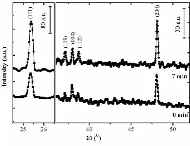
Figure 4. XRD patterns of NTO films deposited at condition of co-sputtered time of 0 and 7 min.
Figure 5 shows the dependence of (αhν)1/2 versus photon energy. At higher photon energy, the linear feature is observed, giving the way to extrapolate the Tauc band gap of the NTO thin films. The extrapolation indicates that the direct band gap value is in the range between 3.25 and 3.42 eV. Dobromir et al. reported that Tauc band gap values of NTO thin films were between 3.27 and 3.45 eV with Nb doped content from 6.7 to 16.2 at% [18]. Our calculated band gap values were equivalent.
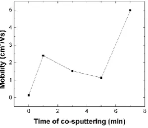
Hall measurement was used to evaluate electrical properties of co-sputtered NTO films after annealing. Figure 6, 7 and 8 show resistivity, carrier concentration, and Hall mobility of co-sputtered NTO films as a function of co-sputtered time. All of electrical properties improved significantly when Nb was added to NTO films. Resistivity decreased and carrier concentration became higher as co-sputtered time decreased. Mobility did not have progressive behavior but also improved. The optimized film was obtained at co-sputtered time of 7 mins, with resistivity of 3.5×10⁻³ Ωcm, carrier concentration of 2.4×1020 cm-3, and Hall mobility of 5.0 cm2V-1s-1. We were successful in fabricating a conductive NTO film by using co-sputter method.
Figure 6. Resistivity of NTO films as a function of Nb co-sputtered time.
Figure 7. Carrier concentration of NTO films as a function of Nb co-sputtered time.
4. Conclusion
In this study, we introduce a co-sputtered process for fabricating low resistive NTO thin films. Nb content at surface area was evaluated by EDX measurement; the results showed that Nb content was increased from 5% to 14% when co-sputtering time raised from 0 to 7 mins. These results confirmed that Nb successfully diffused inside thin films during annealing process. Co-sputtered films after annealing were in anatase polycrystalline phase without any other peak. Electrical properties were significantly improved when Nb was added. The optimized thin film show a resistivity of 3.5×10⁻³ Ωcm, a carrier concentration of 2.4×10²⁰
cm-3, and a Hall mobility of 5.0 cm2V-1s-1. These NTO thin films may be suggested to applications in the low-cost semiconducting oxide based solar cells or heat-resistant coatings on glass windows.
Acknowledgements
The authors greatly acknowledge the financial support of Vietnam National University Hanoi under the project “Fabrication of Nb:TiO2 thin films for smart windows: thermal insulation by reflecting the infrared radiation” through the contract number QG.14.23.
References
[1] D. S. Ginley and C. Bright, Transparent Conducting Oxides, MRS Bull.25 (2000) 15-18.
[2] S. Ishibashi, Y. Higuchi, Y. Ota, and K. Nakamura, Low resistivity indium–tin oxide transparent conductive films. II. Effect of sputtering voltage on electrical property of films,J. Vac. Sci. Technol. A 8 (1990) 1403 [3] R. D. Gordon, Criteria for Choosing Transparent Conductors, MRS Bulletin 25 (2000) 52
[4] Handbook of transparent conductors, edited by David S. Ginley, Hideo Hosono, David C. Paine, Springer, New York, America (2010), pp.8.
[5] Y. Furubayashi, H. Hitosugi, Y. Yamamoto, K. Inaba, G. Kinoda, Y. Hirose, T. Shimada, and T. Hasegawa, A transparent metal: Nb-doped anatase TiO2, Appl. Phys. Lett. 86 (2005) 252101.
[6] N. L. H. Hoang, N. Yamada, T. Hitosugi, J. Kasai, S. Nakao, T. Shimada, and T. Hasegawa, Low-temperature Fabrication of Transparent Conducting Anatase Nb-doped TiO2 Films by Sputtering, Appl. Phys. Express 1
(2008) 115001
[7] D. S. Bhachu, S.Sathasivam, G.Sankar, D. O. Scanlon, G. Cibin, C. J. Carmalt, I. P.Parkin,G. W. Watson, S. M. Bawaked, A. Y. Obaid, S. Al-Thabaiti, and S. N. Basahel, Solution Processing Route to Multifunctional Titania Thin Films: Highly Conductive and Photcatalytically Active Nb:TiO2,Adv. Funct. Mater. 24 (2014) 5075
[8] S.Seegera, K.Ellmerb, M.Weisea, D.Gogovac, D.Abou-Rasb, and R.Mientusa, Reactive magnetron sputtering of Nb-doped TiO2 films: Relationships between structure, composition and electrical properties, Thin Solid Films
605 (2016) 44.
[9] J. Osorio-Guillen, S. Lany, and A. Zunger, Atomic Control of Conductivity Versus Ferromagnetism in Wide-Gap Oxides Via Selective Doping: V, Nb, Ta in Anatase TiO2, Phys. Rev. Lett.100 (2008) 036601.
[10] G. E. Jellison, L. A. Boatner, J. D. Budai, B. S. Jeong and D. P. Norton, Spectroscopic ellipsometry of thin film and bulk anatase(TiO2), J. Appl. Phys. 93 (2003)9537
[11] B. H. Park, L. S. Li, B. J. Gibbons, J. Y. Huang and Q. X. Jia, Photovoltaic response and dielectric properties of epitaxial anatase TiO2 films grown on conductive La0.5Sr0.5CoO3 electrodes, Appl. Phys. Lett. 79 (2001)2797
[12] M. Kambe, K. Sato, D. Kobayashi, Y. Korogawa, S. Miyajima, M. Fukawa, N. Taneda, A. Yamada and M. Konagai, TiO2-Coated Transparent Conductive Oxide (SnO2:F) Films Prepared by Atmospheric Pressure
Chemical Vapor Deposition with High Durability against Atomic Hydrogen,Jpn. J. Appl. Phys.45 (2006) L291 [13] H. Nogawa, T. Hitosugi, H. Kamisaka, K. Yamashita, A. Chikamatsu, K. Yoshimatsu, H. Kumigashira, M.
of Highly Conductive Anatase Ti0.94Nb0.06O2Epitaxial Thin Films, Mater. Res. Soc. Symp. Proc.1074 (2008)
1074-I05-08.
[14] T. Hitosugi, A. Ueda, S. Nakao, N. Yamada, Y. Furubayashi, Y. Hirose, T. Shimada, and T. Hasegawa, Fabrication of highly conductive Ti1−xNbxO2 polycrystalline films on glass substrates via crystallization of
amorphous phase grown by pulsed laser deposition,Appl. Phys. Lett. 90 (2007) 212106
[15] N. Yamada, T. Hitosugi, J. Kasai, N. L. H. Hoang, S. Nakao,Y. Hirose, T. Shimada, and T. Hasegawa, Transparent conducting Nb-doped anatase TiO2 (TNO) thin films sputtered from various oxide targets, Thin Solid
Films 518 (2010) 3101.
[16] N. Yamada, T. Hitosugi, J. Kasai, N. L. H. Hoang, S. Nakao. Y. Hirose, T. Shimada and T. Hasegawa, Direct growth of transparent conducting Nb-doped anatase TiO2 polycrystalline films on glass, J. Appl. Phys. 105
(2009) 123702
[17] D. Mardare, M. Tasca, M. Delibas and G.I. Rusu, On the structural properties and optical transmittance of TiO2
r.f. sputtered thin films, Appl. Surf. Sci 156 (2000) 200.