196 | P a g e
IMPLEMENTATION OF AN EFFICIENT CLASS-AB
OP-AMPS WITH HIGH AND SYMMETRICAL SLEW
RATE USING H-SPICE
P. Ambica Devi
1, V. Srinivasa Rao
21
PG Scholar, Shri Vishnu Engineering College for Women, Bhimavaram, AP, (India)
2Associate Professor, Department of ECE,
Shri Vishnu Engineering College for Women(Autonomous), Bhimavaram, AP, (India)
ABSTRACT
The operational amplifier is widely used in various integrated circuits these days such as in analogue
computers, simulation systems and in many electronic applications as filtering, buffering and comparison of
signal levels. In this paper various schemes of power efficient class AB two stage op-amps with nearly
symmetric slew rate and very simple architectures are introduced. These schemes have been implemented by
using a current replication branch with scaled down transistors in combination with adaptive loads. The
proposed operational amplifier has been implemented by modifying the existing power efficient class AB
two-state op-amps with current replication branch and adaptive loads with symmetrical and high slew rate. The
improved architecture provides maximum output current several times higher than the bias current. Hence it is
used to provide a push-pull output stage with maximum output current. Post layout simulations and
comparisons are made for all these architectures where the proposed circuit has obtained much better slew rate
when compared to the all existing schemes. The circuits presented in this work are analysed by using the
backend tool H-Spice and are designed in 120nm technology.
Keywords: Class-AB Operation, CMOS Analog Integrated Circuit, Operational Amplifier, Slew
Rate
I INTRODUCTION
The designing of op-amps puts new challenges in low power applications because as technology advances the
channel length of the device is reducing day by day. Hence the design of op-amp is becoming a complex task.
Various advancements have been made through new techniques and technology which appeared recently. They
allow us to implement the designs in multiple alternative ways. Involvement of design automation tools that are
used in analog and mixed signal design are yet to be matured as in the case of digital design domain. For EDA
designers, short channel effects in design automation for mixed signal design are also a challenging task.
Designing of two-stage op-amps is a multi dimensional optimization problem because optimizations of one or
more parameters can easily results into degradation of other parameters. To achieve high symmetrical slew rate
197 | P a g e
gain Aol is possible for these schemes. This is the main drawback of single stage op-amps based on this
technique. This is due to the inclusion of the output cascading transistors which are tended to increase the output
resistance Rout for increasing Aol which is open loop gain. But it would seriously limit the maximum output
current and the slew rate enhancement factor.
Conventional single stage class-A miller compensated op-amp is descried initially. Then Two-stage op-amps
with nearly symmetrical slew rate are presented in this brief. Class-AB operation also achieved for these
op-amps but only for static input signals. The coming sections describe other existing and proposed topologies,
simulation results and experimental values respectively. Finally some comparisons and conclusions are drawn
from the obtained results.
II EXISTING CLASS AB TWO-STAGE OP-AMPS
2.1 Conventional Class-A two-stage Miller Compensated Op-Amp
The conventional class-A two stage Miller compensated op-amp which is shown in fig 1(a) is characterized by a
highly asymmetrical slew rate. Its positive slew rate is very much higher than the negative slew rate. Expression
of the negative slew rate is SR- = 2IB/CL. Biasing current is represented by IB and CL is load capacitance. It
has much lower negative slew rate. This is due to the fact that nmos transistor which is placed at the output stage
(MoN) acts as a dc current source. The magnitude of the current source is 2IB. In class-A op-amps the only way
to increase slew rate is by increasing IB. But static power increases with the increment of IB. This is the main
limitation in class-A op-amps. Schematic diagram and transient simulations of the Conventional two-stage
Miller op-amp are shown in fig 1(a) and fig 1(b) respectively.
Fig. 1(a) Schematic diagram of Conventional Class-A two-stage Miller op-amp
198 | P a g e
2.2 Class AB-two Stage Op-amps
Class-AB op-amps avoid this limitation mentioned in A op-amps. There have been reported many
class-AB two-stage op-amps in [5]-[7]. Most of them feature relatively modest effective slew rate improvement. This
improvement in slew rate can be achieved by requiring additional complex circuitry and/or additional static
power dissipation which is non negligible or it can be done by increasing power supply requirements. Current
efficiency (CE) is defined as the ratio of the maximum current at the output (Ioutmax) to the total op-amp static
current (IQtot).The expression of current efficiency is CE= Ioutmax/ IQtot. Additional circuitry added to the
circuit to achieve class-AB operation. So IQtot increases so that current efficiency decrases.
2.2.1 Free Class-AB Op-Amp
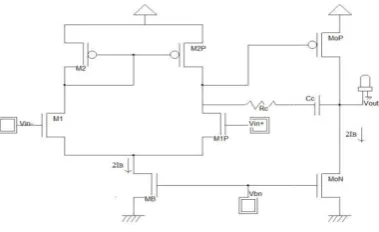
One of the schemes which have been reported in [8] is illustrated here in the fig 2(a). This circuit achieves
class-AB operation. This needs very small additional hardware for achieving class-class-AB operation. This circuit is
designed by adding two components Rlarge and Cbat. Resistive element Rlarge is implemented by a minimum
size diode connected transistor. Capacitor Cbat is of very small value. This combination of Cbat and Rlarge
works as floating battery. And that transfers ac variations which are taking place at the MoP gate to the MoN transistor’s gate terminal. The ouput stage functions like a push-pull amplifier.
Fig. 2(a) Schematic diagram of Free-class AB op-amp
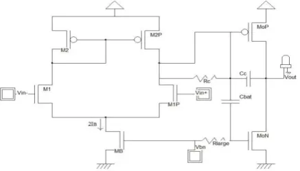
All this process which is due to the additional components Cbat and Rlarge make the circuit to provide dynamic
class-AB operation. This architecture provides large output positive current as well as negative current. The
main advantage of this circuit is power dissipation or supply requirement are same as miller circuit. It does not
need extra supply or increasing power dissipation. But the limitation is it operates only for a certain range of
frequencies where f>1/(2π Rlarge Cbat). When f is more than the upper limit then only this this free class-AB
op-amp works. Schematic diagram and transient simulations of the Free class AB op-amp are shown in fig 2(a)
199 | P a g e
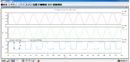
Fig. 2(b) Transient Simulations of Free-class AB op-amp
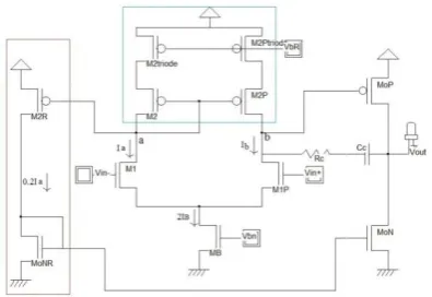
2.2.2 Op-Amp With Current Replication Branch
Class-AB operation can be achieved initially by transforming the output transistor MoN into an active
amplifying device. This is done by simply adding a current replication branch which is formed by two scaled
down transistors M2R and MoNR as shown in fig 3(a). Current replication branch is shown in square box. The
role of this branch is transforming current variations in M1-M2 transistors which is denoted by Ia to the output
transistor MoN, which in turn increases the maximum positive output current by the value twice the bias current
2IB.(which achieved when the transistor MoN is turned off ).
Fig. 3(a) Schematic diagram of Push pull op-amp with current replication branch M2R, MoNR.
Fig. 3(b) Transient Simulations of Push pull op-amp with current replication branch M2R,
MoNR.
This limitation of this circuit is the low value of negative ouput current. The maximum negative current is
200 | P a g e
is that the additional compensation is not required due to current replication branch. It has only one node with
gain, which is in current replication branch and is from the gate terminal to the drain terminal of the transistor
MoN. Miller compensation(with capacitor Cc and Resistance Rc) causes MoP transistor to act as low impedance
diode connected load at the higher frequencies. So the gain (and Miller effect) is reduced between the gate
terminal of MoN (which is denoted by the node Vx) and the output terminal of the op-amp to approximately a
unity value and hence Miller multiplication is prevented by a large factor at node Vx (where Vx is low
impedance node) at large frequencies. Since transistors in current replication branch are downscaled by a factor
of 5, it has negligible dimensions hence reduces static power consumption and area.
Large negative slew rate can be achieved by large negative output currents. But current replication branch
circuit give maximum output current which is limited to only twice the bias current 2IB. So in order to
overcome this limitation and to achieve large negative output currents, non linear adaptive loads can be used
which is similar to the technique introduced in [9] and that reported in paper [10] and also [11]. The
modifications are seen in the coming sections.
Schematic diagram and transient simulations of the Push pull op-amp with current replication branch are
shown in fig 3(a) and fig 3(b) respectively.
2.2.3 Class AB Two-Stage Op-Amp Using Adaptive Loads
Class-AB operation can be achieved by adding an adaptive load to the circuit in the fig 1(a) at the input stage.
Many combinations are possible by adding adaptive loads to the circuits in fig 1(a) and fig 2(a). Two of them
are presented here and are shown by fig 4(a) and fig 5(a). Fig 4(a) is named as adaptive load type II and fig 5(a)
is named as adaptive load type I. In these two cases, the adaptive loads exhibit huge variation of output
resistance between the saturation region and triode region of the transistors M2triode-M2Ptriode. These two
transistors are set at the boundary between ohmic region and constant current region by the biasing voltage VbR
in quiescent conditions. In both schemes, when current in Ia or Ib increases, the transistors M2 triode or
M2Ptriode pulled to go into linear mode (triode mode) hence develop large dain-source voltages. These changes
made because the adaptive loads cause large variations at node voltage a and b, which lead to increase the
maximum current at the output transistors MoP (with the current replication branch) and MoN.
201 | P a g e
Fig 4(b) Transient Simulations of Class AB two-stage op-amp with current replicating branch
using adaptive load II at the input stage.
The performance of the circuits with adaptive loads is nearly similar to the circuit shown in fig 6(a). In this
circuit (fig 6(a)) the adaptive load is directly included in the current replication branch (with scaled down
transistors). This causes extremely large negative output current to flow in output transistors. This circuit is
formed by simply modifying the diode connected load in the current replication branch. Transistor MoNtriode
is included in current replication branch between the gate terminal of transistor MoNR and the lower supply
rails. The required bias voltage is Vbtriode=Vss+VGS+VDSsat=VTH=2VDSsat at gate of MoNR transistor.
Where VDSsat=VGS-VTH is the minimum VDS voltage required to operate in saturation region. To generate it
a small circuit is used. It is formed by using a diode connected transistor MBtriode with W/L ration which is
nearly equal to one fourth of MoNtriode and MoNR. Hence it obtains two times the VDSsat and thus its VGS
voltage is the required Vbtriode voltage. This biasing voltage Vbtriode leaves a quiescent drain-source voltage
for MoNtriode with the value of VDSsat, that causes MoNtriode to be operated (under static conditions) at the
boundary between the ohmic region and constant current regions, similar to M2triode-M2Ptriode as in the fig
4(a) and fig 5(a).When the current in Ia increases gate source voltage of MoNR tend to be increased, and
drain-source voltage of MoNtriode decreases, that brings this transistor into ohmic region and generates consequently
a huge voltage increase at the node Vx and large output current in MoN also be generated correspondingly.
Current through MoN corresponds to negative slew rate hence it increases which is nearly equal to its positive
slew rate.
202 | P a g e
Fig. 5(b) Transient Simulaitons of Class AB two-stage op-amp with current replicating branch
using adaptive load I at the input stage.
Fig. 6(a) Schematic diagram of class AB two-stage op-amp with current replicating branch
using an adaptive load.
Fig. 6(b) Transient Simulations of class AB two-stage op-amp with current replicating branch
using an adaptive load.
“Operational amplifier with current replication branch and adaptive load” is the denotation given to the circuit
in fig 1(f). This circuit has two gain branches but is not harmful for the stability of the circuit in terms of ac
response, and in some cases it is beneficial. The current replication branch is very helpful and compensates the
203 | P a g e
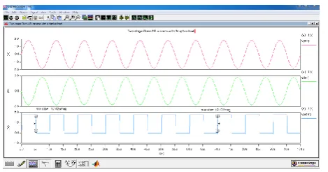
Transient Simulations of op-amps with adaptive load II, adaptive load I and op-amp with adaptive load and
current replication branch are shown in fig 4(b), fig 5(b) and fig 6(b) respectively.
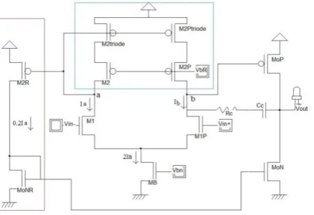
2.3 Proposed Class AB Two- Stage Op-Amp
The proposed operational amplifier has been implemented by modifying the existing power efficient class AB
two-state op-amps with current replication branch and adaptive loads with symmetrical and high slew rate. This
op-amp is denoted by “Class-AB two-stage operational amplifier using two adaptive loads adaptive load 1 and
another adaptive load in current replication branch” and is shown in fig 7(a).
Current replication branch transforms current variations in M1-M2 transistors which is denoted by Ia to the
output transistor MoN, which in turn increases the maximum positive output current by the value twice the bias
current 2IB. Other advantage of this branch is that additional compensation is not required. Large negative slew
rate is achieved by two adaptive loads. One of the adaptive load is directly included in the current replication
branch (Transistor MoNtriode) between the gate terminal of transistor MoNR and the lower supply rails. The
required bias voltage (Vbtriode) for this transistor MoNtriode and the operation is same as the circuit in fig 6(a).
Current through MoN corresponds to negative slew rate hence it increases which is nearly equal to its positive
slew rate. Another load which is connected as is fig 5(a) is responsible for increasing the maximum current at
the output transistors MoP (with the current replication branch) and MoN. The operation of this adaptive load is
similar to the circuit in fig 5(a).
Fig. 7(a) Schematic diagram of Class-AB two-stage operational amplifier using two adaptive
loads adaptive load 1 and another adaptive load in current replication branch
204 | P a g e
Fig. 7(c) Layout of Class-AB two-stage operational amplifier using two adaptive loads adaptive
load 1 and another adaptive load in current replication branch
The improved architecture provides maximum positive and negative output currents (SR+ and SR-) several
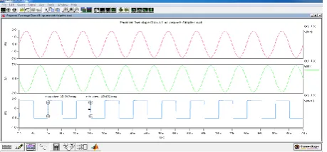
times higher than the previous schemes. Schematic diagram, Transient simulations and the layout of the
Class-AB two-stage operational amplifier with current replication branch using two adaptive loads are shown in fig
7(a), fig 7(b) and fig 7(c) respectively.
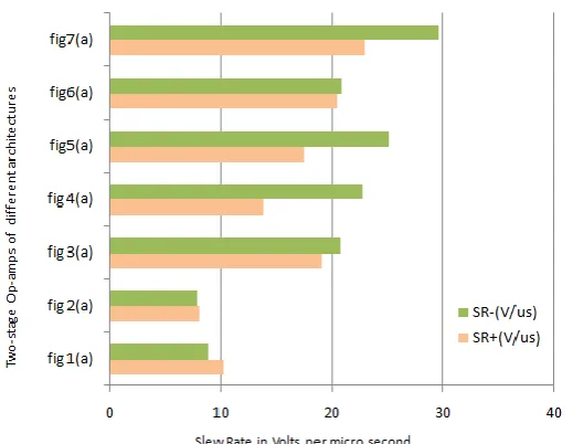
III SIMULATION RESULTS
Post layout simulations and comparisons are made for all these architectures where the proposed circuit has
obtained much better slew rate when compared to the all existing schemes. Slew rate comparison is shown with
the help of the bar graph shown in fig 8(a) where only absolute value of the negative slew rate (SR-) is
mentioned. Here bars correspond to fig 7(a) are the slew rates of the proposed amp (Two stage class-AB
op-amp with current replication branch using two adaptive loads) which are higher than all the previous circuits.
Fig 8(a) Bar graph comparing slew rates of different op-amps
Performance comparison table represents measured values of all the schemes are shown in table 1 where slew
rates are improved for the proposed op-amp. The circuits presented in this work are analysed by using the
205 | P a g e
Table1. Performance comparison
Type of op-amp Technology SR+
(V/us)
SR-(V/us)
Conventional two-stage Miller
op-amp
120nm 10.207 -8.9565
Free class AB op-amp 120nm 8.0624 -7.9303
Push pull op-amp with current
replication branch
120nm 19.018 -20.805
Class AB two-stage op-amp with
current replication branch using
adaptive load II
120nm 13.89 -22.831
Class AB two-stage op-amp with
current replication branch using
adaptive load I
120nm 17.567 -25.07
Class AB two-stage op-amp with
current replication branch using an
adaptive load
120nm 20.424 -20.859
Class-AB two-stage operational
amplifier using two adaptive loads
adaptive load 1 and another
adaptive load in current replication
branch
120nm 23.017 -29.572
IV CONCLUSION
An efficient class AB two-stage op-amp with current replication branch using two adaptive load has been
implemented. It has been tested experimentally and compared with the various schemes of two-stage op-amps.
The measured results show that it has achieved better performance in terms of slew rate. So it can be concluded
that it is advantageous to include two adaptive loads one adaptive load directly in the current replication branch
206 | P a g e
REFERENCES
[1] Jesus Aguado-Ruiz, Antonio Lopez-Martin, Javier Lopez-Lemus, and Jaime Ramirez-Angulo, “Power Efficient
Class AB Op-AmpsWith High and Symmetrical Slew Rate”, IEEE Trans. Very Large Scale Integration (VLSI)
Systtems, vol. 22, no. 4, April 2014.
[2] J. Ramirez-Angulo and M. Holmes, “Simple technique using local CMFB to enhance slew rate and bandwidth of
one-stage CMOS op-amps,” Electron. Lett., vol. 38, no. 23, pp. 1409–1411, Nov. 2002.
[3] A. J. López-Martín, S. Baswa, J. Ramirez-Angulo, and R. G. Carvajal, “Low-voltage super class AB CMOS OTA
cells with very high slew rate and power efficiency,” IEEE J. Solid-State Circuits, vol. 40, no. 5, pp. 1068–1077,
May 2005.
[4] J. A. Galan, A. J. Lopez-Martin, R. G. Carvajal, J. Ramirez-Angulo, and C. Rubia, “Super Class-AB OTAs with
adaptive biasing and dynamic output current scaling,” IEEE Trans. Circuits Syst. I, Reg. Papers, vol. 54, no. 3, pp.
449–457, Mar. 2007.
[5] W. Sansen, “Class AB and driver amplifiers,” in Analog Design Essentials, W. Sansen, Eds., 1st ed. New York,
NY, USA: Springer-Verlag, 2006, pp. 337–362.
[6] C. K. Chava and J. Silva-Martinez, “A frequency compensation scheme for LDO voltage regulators,” IEEE Trans.
Circuits Syst. I, Reg. Papers, vol. 51, no. 6, pp. 1041–1050, Jun. 2004.
[7] D. M. Monticelli, “A quad CMOS single-supply op-amp with rial to rail output swing,” IEEE J. Solid-State
Circuits, vol. 21, no. 6, pp. 1026–1034, Jun. 1986.
[8] K. J. De Langen and J. H. Huising, “Compact low-voltage powerefficient operational amplifier cells for VLSI,”
IEEE J. Solid-State Circuits, vol. 33, no. 10, pp. 1482–1496, Oct. 1998.
[9] J. Ramirez-Angulo, R. G. Carvajal, A. Lopez-Martin, and J. A. Galan, “A free but efficient class AB two-stage
operational amplifier,” IEEE Trans. Circuits Syst. II, Exp. Briefs, vol. 53, no. 7, pp. 568–571,
Jul. 2006.
[10] J. Ramírez-Angulo, “A novel slew-rate enhancement technique for one stage operational amplifiers,” in Proc.
IEEE 39th Midwest Symp. Circuits Syst., vol. 1. Aug. 1996, pp. 7–10.
[11] F. You, S. H. K. Embabi, and E. Sanchez-Sinencio, “Low-voltage Class-AB buffers with quiescent current
control,” IEEE J. Solid-State Circuits, vol. 33, no. 6, pp. 915–920, May 1998.
[12] J. Ramírez-Angulo, R.G. Carvajal, J. Tombs, and A. Torralba, “Low-voltage CMOS op-amp with rail-to-rail
input and output signal swing for continuous-time signal processing using multiple-input
floating-gate transistors,” IEEE Trans. Circuits Syst. II, Analog Digital Signal Process., vol. 48, no. 1, pp. 111–117,
Jan. 2001.
[13] R. Eschauzier and J. Huijsing, Frequency Compensation Techniques for Low-Power Operational Amplifiers.
Norwell, MA, USA: Kluwer, 1995.
[14] G. Palumbo and S. Pennisi, “Design methodology and advances in nested Miller compensation,” IEEE Trans.
Circuits Syst. I, Fundam. Theory Appl., vol. 49, no. 7, pp. 893–903, Jul. 2002.
[15] S. Sakurai, S. R. Zarabadi, and M. Ismail, “Folded-cascode CMOS operational amplifier with slew rate
enhancement circuit,” in Proc. IEEE Int. Symp. Circuits Syst., vol. 4. May 1990, pp. 320–3208.
[16] C. H. Lin and M. Ismail, “A low-voltage CMOS rail-to-rail class-AB input/output opamp with slew-rate and