IJIRT 145292
INTERNATIONAL JO URNAL OF INNOVATIVE RESEARCH IN TECHNOLOGY407
Implementation of High Speed and Energy Efficient
Carry Skip Adder
Miss. Pranita R.Bujadkar
1, Prof. N N Gyanchandani
2 1PG Scholar, Dept. of E&TC, J.D College of Engineering and Management, Nagpur
2
Professor, Dept. of E&TC, J.D College of Engineering and Management, Nagpur
Abstract-
In this paper we design carry skip adder for
the purpose of lower energy consumption and it gives higher speed. The main function is that improves the delay, it is also known as carry bypass adder. The carry skip adder is that improves the delay of ripple carry adder with less effort compared with the other adder. Also the improvement in the worst-case delay is achieved by using various carry-skip adders to form a block-carry-skip adder. In this paper we shown that efficient carry skip adder in terms speed enhancement and it can be achieved by various method such as concatenation and increme ntation method. Also i n addition, instead of using multiplexer logic, the proposed scheme makes use of AND OR Invert and OR AND Invert compound gate for the skip logic.AND OR Invert logic gates and AOI are basically two level compound logic functions constructed by or from the combination of one or more AND gates followed by a NOR gate. Also these gates can be easily implemented in CMOS circuitry. And or gates are particularly better than the total number of transistors or gate less than if the AND, NOT and OR functions were implemented separately. These results are in increased speed, reduced power, smaller area and potentially lower fabrication cost. And the results can be obtained by various tools such as Xilinx and Modesim 6.4b. Using this we can improves the delay on an average of 45% and the energy will be minimum 39%. Using CS KA we can achieve reduction power consumption compared with latest works in the field.
Index Terms- AOI, OAI, CS KA, RCA, PPA, CS LA
I. INTRODUCTION
Adder is known as digital circuit which performs addition of numbers. In so many computers and other kind of processors adders are used in the arithmetic logic units. Adders are also utilized in other parts of the processor, such as they are used to calculate addresses, table indices, increment and decrement operators, and similar operations. In our paper, gives
IJIRT 145292
INTERNATIONAL JO URNAL OF INNOVATIVE RESEARCH IN TECHNOLOGY408
whereas its area and power consumption are similarto those of the RCA.
In addition to the power-delay product of the CSKA is smaller than those of the CSLA and PPA structures. And due to the small number of transistors, the CSKA benefits from relatively short wiring lengths as well as a regular and simple layout. It gives comparatively lower speed of this adder structure, however, limits its use for high-speed applications. Therefore in our paper, given the attractive features of the CSKA structure, we have focused on reducing its delay by modifying its implementation based on the static CMOS logic. The concentration on the static CMOS originates from the desire to have a reliably operating circuit under a wide range of supply voltages in highly scaled technologies. The proposed modification increases the speed considerably while maintaining the low area and power consumption features of the CSKA.
Hence, the contributions of this paper can be summarized as follows.
1.Proposing a modified CSKA structure by
combining the concatenation and the incrimination schemes to the conventional CSKA (Conk-CSKA) structure for enhancing the speed and energy efficiency of the adder. These modification provides us with the ability to use simpler carry skip logics based on the A-O Invert/O-A Invert compound gates instead of the multiplexer.
2. Providing a design strategy for constructing an efficient CSKA structure based on analytically expressions presented for the critical path delay. 3. Investigate the impact of voltage scaling on the efficiency of the proposed CSKA structure from the nominal supply voltage to the near-threshold voltage 4. Proposing a hybrid variable latency CSKA structure based on the extension of the suggested CSKA, by replacing some of the middle stages in its structure with a PPA.
II. RESEARCH METHODOLOGY
The conventional structure of CSKA consists of many stages containing chain of full adders blocks of RCA and 2:1 multiplexer carry skip logic. The RCA blocks are connected to each other throug h 2:1 multiplexers, which can placed into one or more level structures. The CSKA configuration the number of
the FAs per stage has a great impact on the speed of this type of adder. The structure of an N -bit Conventional CSKA, which is based on blocks of the RCA blocks as shown in Fig. 1. In addition to the chain of Full adder in each stage, there is a carry skip logic. For an Ripple carry adder that contains N cascaded FAs, the worst propagation delay of the summation of two N bit numbers, A and B belongs to the case where all the FAs are in the propagation mode. It means that worst case delay belongs to the case where Qi is the propagation signal related to Ai and Bi . This is shows that the delay of the RCA is linearly related to N. the N FAs of the CSKA are grouped in Q stages. Each stage contains an RCA block with M j FAs ( j = 1,….P) and a skip logic. In each stage, the inputs of the multiplexer (skip logic) are the carry input of the stage and the carry output of its RCA block (FA chain). In addition, the product of the propagation signals of the stage is used as the selector signal of the multiplexer.
The CSKA may be implemented using FSS and VSS where the highest speed may be obtained for the VSS structure in charge of your proceedings see author-kit message for contact info
Figure1: Conventional structure of CSKA
1. Fixed Stage Size CSKA:
By assuming that each stage of the CSKA contains MFAs, there are Q=N/M stages where for the sake of simplicity, we assume Q is an integer. The input signals of the jth multiplexer are the carry output of the FAs chain in the j-th stage denoted by C0j, the carry output of the previous stage (carry input of the j-th stage) denoted by C1j.
The critical path of the CSKA contains three parts: 1. The path of the FA chain of the first stage whose delay is equal to M×TCARRY;
2. The path of the intermediate carry skip multiplexer whose delay is equal to the (Q–1)×TMUX;
IJIRT 145292
INTERNATIONAL JO URNAL OF INNOVATIVE RESEARCH IN TECHNOLOGY409
that TCARRY, TSUM, and TMUX are thepropagation delays of the carry output of an FA, the sum output of an FA, and the output delay of a 2:1 multiplexer, respectively. Hence, the critical path delay of a FSS CSKA is formulated by
Based on (1), the optimum value of M (M opt) that leads to optimum propagation delay may be calculated as(0.5Nα)1/2 where α is equal to
TMUX/TCARRY. Therefore, the optimum
propagation delay (TD, opt) is obtained from
2. Variable Stage Size CSKA:
As mentioned before, by assigning variable sizes to the stages, the speed of the CSKA may be improved. The speed improvement in this type is achieved by lowering the delays of the first and third terms in (1). These delays are minimized by lowering sizes of first and last RCA blocks. For instance, the first RCA block size may be set to one, whereas sizes of the following blocks may increase. To determine the rate of increase, let us express the propagation delay of the C1j (t1j) by
Where t0j−1(t1j−1) shows the calculating delay of C0j−1(C1j−1) signal in the (j −1)th stage. In a FSS CSKA, except in the first stage, t0j is smaller than t1j. Hence, based on (3), the delay of t0j−1 may be increased from t01 to t1j−1 without increasing the delay of C1j signal. This means that one could increase the size of the (j −1)th stage (i.e., Mj−1) without increasing the propagation delay of the CSKA. Therefore, increasing the size of Mj for the jth stage should be bounded by
The structure is based on combining the
concatenation and the incrementation schemes with the Conv-CSKA structure, and hence, is denoted by CI-CSKA. It provides us with the ability to use simpler carry skip logics. The logic replaces 2:1 multiplexers by AOI/OAI compound gates. The
gates, which consist of fewer transistors, have lower
delay, area, and smaller power consumption
compared with those of the 2:1 multiplexer. Note that, in this structure, as the carry propagates through the skip logics, it becomes complemented. Therefore, at the output of the skip logic of even stages, the complement of the carry is generated. The structure has a considerable lower propagation delay with a slightly smaller area compared with those of the conventional one. Note that while the power consumptions of the AOI (or OAI) gate are smaller than that of the multiplexer, the power consumption of the proposed CI-CSKA is a little more than that of the conventional one. This is due to the increase in the number of the gates, which imposes a higher wiring capacitance (in the noncritical paths). Now, we describe the internal structure of the proposed CI-CSKA shown in below Fig. in more detail. The adder contains two N bits inputs, A and B, and Q stages.
Figure2. Proposed Ci-CSKA Structure.
IJIRT 145292
INTERNATIONAL JO URNAL OF INNOVATIVE RESEARCH IN TECHNOLOGY410
{ZKj+Mj,...,ZKj+2,ZKj+1} for Kj =Σ j−1r=1 Mr(j = 2,...,Q)],and also Cj signals. In the proposed structure, the first stage has only one block, which is RCA. The stages 2 to Q consist of two blocks of RCA and incrementation.
3. Area and Delay of the Proposed Structure: As mentioned before, the use of the static AOI and OAI gates (six transistors) compared with the static 2:1 multiplexer (12 transistors), leads to decreases in the area usage and delay of the skip logic. In addition, except for the first RCA block, the carry input for all other blocks is zero, and hence, for these blocks, the first adder cell in the RCA chain is a HA. This means that (Q−1) FAs in the conventional structure are replaced with the same number of HAs in the suggested structure decreasing the area usage. In addition, note that the proposed structure utilizes incrementation blocks that do not exist in the conventional one. These blocks, however, may be implemented with about the same logic gates (XOR and AND gates) as those used for generating the select signal of the multiplexer in the conventional structure.
Therefore, the area usage of the proposed CI-CSKA structure is decreased compared with that of the conventional one. The critical path of the proposed CI-CSKA structure, which contains three parts. These parts include the chain of the FAs of the first stage, the path of the skip logics, and the incrementation block in the last stage. The delay of this path (TD) may be expressed as
Where the three brackets correspond to the three parts mentioned above, respectively. Here, TAND and TXOR are the delays of the two inputs static AND and XOR gates, respectively. Note that, [(Mj −1) TAND+TXOR] shows the critical path delay of the jth incrementation block (TINC,j). To calculate the delay of the skip logic, the average of the delays of the AOI and OAI gates, which are typically close to one another [35], is used. Thus, may be modified.
Where TAOI and TOAI are the delays of the static AOI and OAI gates, respectively. The comparison of (1) and (11) indicates that the delay of the proposed structure is smaller than that of the conventional one. The First reason is that the delay of the skip logic is considerably smaller than that of the conventional structure while the number of the stages is about the same in both structures. Second, since TAND and TXOR are smaller than TCARRY and TSUM, the third additive term in (11) becomes smaller than the third term in (1). It should be noted that the delay reduction of the skip logic has the largest imp act on the delay decrease of the whole structure.
1. The size of the RCA block of the first stage is one. 2. From the second stage to the nucleus stage, the size of jth stage is determined based on the delay of the product of the sum of its RCA block and the delay of the carry output of the (j −1)th stage. Hence, based on the description, the size of the RCA block of the jth stage should be as large as possible, while the delay of the product of the it’s output sum should be smaller than the delay of the carry output of the (j −1)th stage. Therefore, in this case, the sizes of the stages are either not changed or increased.
IJIRT 145292
INTERNATIONAL JO URNAL OF INNOVATIVE RESEARCH IN TECHNOLOGY411
(13)5. Finally, note that, it is possible that the sum of all the stage sizes does not become equal to N. In the case, where the sum is smaller than N by d bits, we should add another stage with the size of d. The stage is placed close to the stage with the same size. In the case, where the sum is larger than N by d bits, the size of the stages should be revised (Step 3). For more details on how to revise the stage size
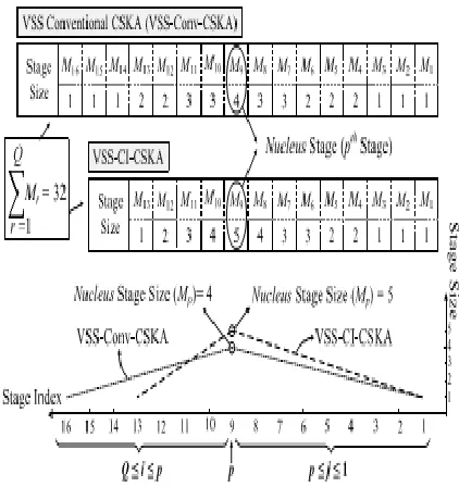
Now, the procedure for determining the stage sizes is demonstrated for the 16-bit adder. It includes both the conventional and the proposed CI-CSKA structures. The number of stages and the corresponding size for each stage, which are given in Fig. 4, have been determined based on a 45-nm static CMOS technology. The dashed and dotted lines in the plot indicate the rates of size increase and decrease. While the increase and decrease rates in the conventional structure are balanced, the decrease rate is more than the increase one in the case of the proposed structure.
Figure3. Sizes of The Stages.
In The Case Of Vss for the Proposed and Conventional 16-Bit CSKA Structures in 45-Nm Static Cmos Technology. It originates from the fact that, in the Conv-CSKA structure, both of the stages size increase and decrease is determined based on the RCA block delay while in the proposed CI-CSKA structure, the increase is determined based on the RCA block delay and the decrease is determined
based on the incrementation block delay. The imbalanced rates may yield a larger nucleus stage an d smaller number of stages leading to a smaller propagation delay.
4. Proposed Hybrid Variable Latency CSKA:
In this section, a hybrid variable latency CSKA structure based on the CI-CSKA structure is proposed.
i) Proposed Hybrid Variable Latency CSKA
Structure:
The basic idea behind using VSS CSKA structures was based on almost balancing the delays of paths such that the delay of the critical path is minimized compared with that of the FSS structure. This deprives us from having the opportunity of using the slack time for the supply voltage scaling. To provide the variable latency feature for the VSS CSKA structure, we replace some of the middle stages in our proposed structure with a PPA modified in this paper. It should be noted that since the Conv -CSKA structure has a lower speed than that of the proposed one, in this section, we do not consider the conventional structure. The proposed hybrid variable latency CSKA structure where an Mp-bit modified PPA is used for the pth stage (nucleus stage). Since the nucleus stage, which has the largest size (and delay) among the stages, is present in both SLP1 and SLP2, replacing it by the PPA reduces the delay of the longest.
IJIRT 145292
INTERNATIONAL JO URNAL OF INNOVATIVE RESEARCH IN TECHNOLOGY412
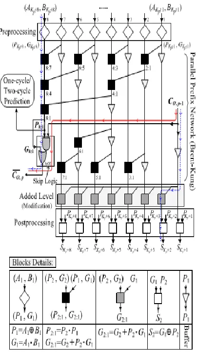
Figure ii): Internal Structure of the pth Stage of theProposed Hybrid Variable Latency CSKA.
Thus, the use of the fast PPA helps increasing the available slack time in the variable latency structure. It should be mentioned that since the input bits of the PPA block are used in the predictor block, this block becomes parts of both SLP1 and SLP2. In the proposed hybrid structure, the prefix network of the Brent–Kung adder is used for constructing the nucleus stage. One the advantages of the this adder compared with other prefix adders is that in this structure, using forward paths, the longest carry is calculated sooner compared with the intermediate carries, which are computed by backward paths. In addition, the fan-out of adder is less than other parallel adders, while the length of its wiring is smaller. Finally, it has a simple and regular layout. The internal structure of the stage p, including the modified PPA and skip logic.
Note that, for this figure, the size of the PPA is assumed to be 8 (i.e.,Mp=8). As shown in the figure, in the preprocessing level, the propagate signals (Pi) and generate signals (Gi)for the inputs are calculated. In the next level, using Brent–Kung parallel prefix network, the longest carry (i.e., G8:1) of the prefix network along with P8:1, which is the product of the all propagate signals of the inputs, are calculated sooner than other intermediate signals in this network. The signal P8:1 is used in the skip logic to determine if the carry output of the previous stage (i.e., CO,p−1) should be skipped or not. In addition, this signal is exploited as the predictor signal in the variable latency adder. It should be mentioned that all of these operations are performed in parallel with other stages. In the case, whereP8:1is one, CO,p−1should skips this stage predicting that some critical paths are activated. On the other hand, when P8:1 is zero, CO.
In addition, no critical path will be activated in this
case. After the parallel prefix network, the
intermediate carries, which are functions ofCO,p −1 and intermediate signals, are computed. Finally, in the post processing level, the output sums of this stage are calculated. It should be noted that this implementation is based on the similar ideas of the concatenation and incrementation concepts used in the CI-CSKA discussed. It should be noted that the end part of the SPL1 path fromCO,p−1 to final summation results of the PPA block and the beginning part of the SPL2 paths from inputs of this block to CO,P belong to the PPA block. In addition, similar to the proposed CI-CSKA structure, the first point of SPL1 is the first input bit of the first stage, and the last point of SPL2 is the last bit of the sum output of the incrementation block of the stage-Q. The steps for determining the sizes of the stages in the hybrid variable latency CSKA structure are similar to the ones. Since the PPA structure is more efficient when its size is equal to an integer power of two, we can select a larger size for the nucleus stage accordingly.
IJIRT 145292
INTERNATIONAL JO URNAL OF INNOVATIVE RESEARCH IN TECHNOLOGY413
III. RESULTS Simulation Results:
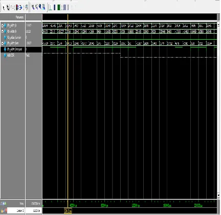
In this project architecture is designed by Verilog HDL, this is simulated by using Modelsim6.4b, verifiy the functionality. We have verified the functionality for 32 bit. Below fig shows the addition of two 32 bit numbers.
Figure a): Simulation Results.
3.1 Simulation Results:
In this project architecture is designed by Verilog HDL, this is simulated by using Modelsim6.4b, verifiy the functionality. We have verified the functionality for 32 bit. Below fig shows the addition of two 32 bit numbers.
Figure 3.1(a): Simulation Results.
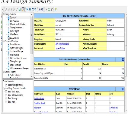
3.2 Synthesis Results:
The developed project is simulated and verified their functionality. Once the functional verification is done, the RTL model is taken to the synthesis process using the Xilinx ISE tool. In synthesis process, the RTL model will be converted to the gate level netlist mapped to a specific technology library. Here in this Spartan 3E family, many different devices were available in the Xilinx ISE tool. In order to synthesis this design the device named as “XC3S500E” has been chosen and the package as “FG320” with the device speed such as “-4”.
This design is synthesized and its results were analyzed as follows.
RTL Schematic:
Figure 3.2(a): RTL Schematic.
3.3 Technology Schematic:
IJIRT 145292
INTERNATIONAL JO URNAL OF INNOVATIVE RESEARCH IN TECHNOLOGY414
3.4 Design Summary:Figure 3.4(a): Design Summary.
IV. CONCLUSION
In this paper, a static CMOS CSKA structure called CI-CSKA was proposed, which exhibits a higher speed and lower energy consumption compared with those of the conventional one. The speed enhancement was achieved by modifying the
structure through the concatenation and
incrementation techniques. In addition, AOI and OAI compound gates were exploited for the carry skip logics. The efficiency of the proposed structure for both FSS and VSS was studied by comparing its power and delay with those of the Conv -CSKA, RCA, CIA, SQRT-CSLA, and KSA structures. The results revealed considerably lower PDP for the VSS implementation of the CI-CSKA structure over a wide range of voltage from super-threshold to near threshold.
The results also suggested the CI-CSKA structure as a very good adder for the applications where both the speed and energy consumption are critical. In addition, a hybrid variable latency extension of the structure was proposed. It exploited a modified parallel adder structure at the middle stage for increasing the slack time, which provided us with the opportunity for lowering the energy consumption by reducing the supply voltage. The efficacy of this structure was compared versus those of the variable latency RCA, C2SLA, and hybrid C2SLA structures. Again, the suggested structure showed the lowest delay and PDP making itself as a better candidate for high-speed low-energy applications.
REFERENCES
[1] I. Koren, Computer Arithmetic Algorithms, 2nd ed. Natick, MA, USA: A K Peters, Ltd., 2002. [2] R. Zlatanovici, S. Kao, and B. Nikolic, “Energy–
delay optimization of 64-bit carry-look ahead adders with a 240 ps 90 nm CMOS design example,” IEEE J. Solid-State Circuits, vol. 44, no. 2, pp. 569–583, Feb. 2009.
[3] S. K. Mathew, M. A. Anders, B. Bloechel, T. Nguyen, R. K. Krishnamurthy, and S. Borkar, “A 4-GHz 300-mW 64-bit integer execution ALU with dual supply voltages in 90-nm CMOS,” IEEE J. Solid-State Circuits, vol. 40, no. 1, pp. 44–51, Jan. 2005.
[4] V. G. Oklobdzija, B. R. Zeydel, H. Q. Dao, S. Mathew, and R. Krishnamurthy, “Comparison of high-performance VLSI adders in the energy-delay space,” IEEE Trans. Very Large Scale Integr. (VLSI) Syst., vol. 13, no. 6, pp. 754–758, Jun. 2005.
[5] B. Ramkumar and H. M. Kittur, “Low-power
and area-efficient carry select adder,”IEEE Trans. Very Large Scale Integr. (VLSI) Syst., vol. 20, no. 2, pp. 371–375, Feb. 2012.
[6] M. Vratonjic, B. R. Zeydel, and V. G.
Oklobdzija, “Low- and ultra low-power
arithmetic units: Design and comparison,” in Proc. IEEE Int. Conf. Comput. Design, VLSI Comput. Process. (ICCD), Oct. 2005, pp. 249– 252.
[7] C. Nagendra, M. J. Irwin, and R. M. Owens, “Area-time-power tradeoffs in parallel adders,” IEEE Trans. Circuits Syst. II, Analog Digit. Signal Process., vol. 43, no. 10, pp. 689–702, Oct. 1996.
[8] Y. He and C.-H. Chang, “A power-delay
efficient hybrid carry look ahead/carry-select based redundant binary to two’s complement converter,” IEEE Trans. Circuits Syst. I, Reg. Papers, vol. 55, no. 1, pp. 336–346, Feb. 2008. [9] C.-H. Chang, J. Gu, and M. Zhang, “A review of