c:
•
RESEARCH, INC.
eRA Y PROPRIETARY
CRAY® COMPUTER SYSTEMS
CRAY X-MP/1 SYSTEM
PROGRAMMER REFERENCE MANUAL
CSM0111000
-...
Ii:::ti~~
RECORD OF REVISION RESEARCH. INC. PUBLICATION NUMBER CSMOIII000
Each time this manual is revised and reprinted, all changes issued against the previous version are incorporated into the new version and the new version is assigned an alphabetic level.
Every page changed by a reprint with revision has the revision level in the lower righthand corner. Changes to part of a page are noted by a change bar in the margin directly opposite the change. A change bar in the margin opposite the page number indicates that the entire page is new. If the manual is rewritten, the revision level changes but the manual does not contain change bars.
Requests for copies of Cray Research, Inc. publications should be directed to Logistics and comments about these publications should be directed to:
CRAY RESEARCH, INC. ATTENTION: Publications 890 Industrial Blvd.
Technical Operations Building Chippewa Falls, WI 54729
i i
Revision Description
July 1984 - Original printing.
A November 1985 - Reprint with revision. Memory addressing
formats and Exchange Package changes for 64K-chip systems and
8-million-word memories were added. The Gather/scatter,
compressed index, and the 24-bit immediate constant load
instructions were also added. Numerous editorial changes and
corrections were also made. This revision obsoletes all
previous printings.
B August 1986 - Reprint with revision. Corrections were made to
the SECDED maintenance mode function statement documentation and
the underflow detection statement. Additions were made to the
scalar reference hold issue condition and the vector load
information. The clock period (CP) time on serial number 326
and above has been upgraded from 9.~-ns to 8.5-ns. Numerous
technical and editorial changes and corrections were also made. This revision obsoletes all previous printings.
June 1987 - This manual has been converted to a system programmer reference manual to protect Cray propriety
information. When ordering this manual, use publication
number CSM0111000.
CRAY, CRAY-l, and SSD are registered trademarks and APML, CFT, CFT77, CFT2, COS, CRAY-2, CRAY X-MP, CSIM, IDS, SEGLDR, SID, SUPERLINK/ISP,
and UNICOS are trademarks of Cray Research, Inc. The UNICOS system is
derived form the AT&T UNIX system; UNIX is a registered trademark of AT&T.
PREFACE
This manual describes the functions of CRAY X-MP series single-processor
computer systems. It is written to assist programmers and engineers and
assumes a familiarity with digital computers.
This manual describes the overall computer system, its configurations,'
and equipment. It also describes the operation of the Central Processing
Unit (CPU) that executes instructions, provides memory protection, and reports hardware exceptions within the computer systems.
The following publications give details of the I/O Subsystem (lOS), the disk storage units (DSUs), and the SSD solid-state storage device:
HR-0030 HR-0031 HR-0630 HR-0077
I/O Subsystem Hardware Reference Manual
Solid-state Storage Device Hardware Reference Manual Mass Storage Subsystem Hardware Reference Manual Disk Systems Hardware Reference Manual
/ / / / / / / / / / / / / / / / / / / / / / / / / / / / / / / / / / / / / / / / / / / / / / / / / / / / / / /
WARNING
This equipment generates, uses, and can radiate radio frequency energy and if not installed and used in accordance with the instructions manual, may cause
interference to radio communications. It has been
tested and found to comply with the limits for a
Class A computing device pursuant to Subpart J of Part 15 of FCC Rules, which are designed to provide
reasonable protection against such interference when
operated in a commercial environment. Operation of
this equipment in a residential area is likely to cause interference, in which case, the user at his own
expense will be required to take whatever measures may be required to correct the interference.
/ / / / / / / / / / / / / / / / / / / / / / / / / / / / / / / / / / / / / / / / / / / / / / / / / / / / / / /
CONTENTS
PREFACE. . . • • • . . . • . • • • . . . . . i i i
1.
2.
iv
SYSTEM DESCRIPTION .
CONVENTIONS Italics
.
... . . .
.
.
.
.
.
. . .
. .
Register conventions . . . . . Number conventions . . . . . Clock period . . . .
SYSTEM COMPONENTS . . . . .
Central Processing Unit Interfaces . . . . .
1/0 Subsystem
Disk storage units .
Solid-state Storage Device . Condensing units . . . . Power distribution units . Motor-generator units SYSTEM CONFIGURATION . . . . .
CPU RESOURCES
CENTRAL MEMORY . .
Memory organization . . . • • . . • • .
Memory addressing . . . • . . . .
Memory addressing for 16-bank, 16K-chip, 1- and 2-million-word system . . . . • • • • . • .
Memory addressing for 32-bank, 16K-chip,
4-million-word system . . . . . . • • • . . .
Memory addressing for 16-bank, 64K-chip,
4-million-word system. . . . . . . • . • . . . . • . . . .
Memory addressing for 32-bank, 64K-chip,
8-million-word system . . . .
Memory access . • . .
Conflict resolution . Memory access priorities
16-bank phasing . . . .
Memory error correction
1-1 1-4 1-4 1-4 1-4 1-4 1-5 1-5 1-7 1-8 1-10 1-11 1-12 1-13 1-14 1-15 2-1 2-1 2-2 2-3 2-3 2-3 2-3 2-3 2-5 2-7 2-7 2-7 2-8
2. CPU RESOURCES (continued)
3.
INTER-CPU COMMUNICATION SECTION
CPU
Real-time clock
Inter-CPU communication and control
Shared Address and Shared Scalar registers Semaphore registers . . . • . . INPUT/OUTPUT SECTION {Maximum Configuration} Data transfer for Solid-state Storage Device Data transfer for I/O Subsystem
6 Mbyte per second channels
6 Mbyte per second channel operation . • . . .
Input channel programming . . . .
Input channel error conditions . . . . Output channel programming . . . • . .
Programmed Master Clear to external device . . • . . Memory access
I/O lockout
Memory bank conflicts I/O memory conflicts . . . I/O memory request conditions
I/O memory addressing . . . .
CPU CONTROL SECTION
INSTRUCTION ISSUE AND CONTROL
Program Address register . . . . • • .
Next Instruction Parcel register . Current Instruction Parcel register Lower Instruction Parcel register Instruction buffers
EXCHANGE MECHANISM . . . . Exchange Package . . . . .
Processor number Memory error data . Program Address register Memory field registers Mode register . . . . Vector not used (VNU) . . .
Enable second vector logical (ESVL)
Flag register . . . . Exchange Address register . . • .
Enhanced addressing mode (EAM) • • . . . • . •
Data Base Address register
Program State register • . . . .
Cluster Number register . . . • . .
Data Limit Address register . . • • .
A registers . • . . . . . • • • .
S registers • • . . . .
Active Exchange Package . . . •
CSM0111000 CRAY PROPRIETARY
4.
vi
EXCHANGE MECHANISM (continued)
Exchange sequence . . . • . . . . Exchange initiated by deadstart sequence Exchange initiated by Interrupt flag set Exchange initiated by program exit
Exchange sequence issue conditions Exchange Package management
MEMORY FIELD PROTECTION . . . .
Instruction Base Address register Instruction Limit Address register Data Base Address register •
Data Limit Address register Program range error
Operand range error PROGRAMMABLE CLOCK . .
Instructions . . . . . Interrupt Interval register Interrupt Countdown counter
Clear programmable clock interrupt PERFORMANCE MONITOR
DEADSTART SEQUENCE . .
CPU COMPUTATION SECTION
OPERATING REGISTERS ADDRESS REGISTERS
A registers B registers SCALAR REGISTERS . .
S registers T registers VECTOR REGISTERS .
V registers
request .
V register reservations and chaining . • . •
Vector control registers . • • . . . .
Vector Length register Vector Mask register
FUNCTIONAL UNITS . • . . . • . . . • . Address functional units . .
Address Add functional unit . Address Multiply functional unit
Scalar functional units . . . • .
Scalar Add functional unit . • . .
Scalar Shift functional unit • . . • . •
Scalar Logical functional unit . . • . • . • . .
Scalar Population/Parity/Leading Zero functional unit
Vector functional units . . . .
Vector functional unit reservation
3-14 3-14 3-14 3-14 3-15 3-15 3-16 3-17 3-17 3-17 3-18 3-19 3-19 3-19 3-19 3-20 3-20 3-21 3-21 3-21 4-1 4-3 4-3 4-3 4-6 4-6 4-7 4-9 4-9 4-9 4-12 4-13 4-13 4-13 4-14 4-14 4-15 4-15 4-15 4-15 4-16 4-16 4-16 4-16 4-17
5.
FUNCTIONAL UNITS (continued)
Vector Add functional unit . . . • . . . .
Vector Shift functional unit . • . .
Full Vector Logical functional unit . . . . • . . . . Second Vector Logical functional unit . . . • . . Vector Population/Parity functional unit
Floating-point functional units . . . .
Floating-point Add functional unit
Floating-point Multiply functional unit . . Reciprocal Approximation functional unit
ARITHMETIC OPERATIONS . . . .
Integer arithmetic . . . .
Floating-point arithmetic . . . . .
Normalized floating-point numbers . . . . .
Floating-point range errors . . . .
Double-precision numbers . . . . .
Addition algorithm
Multiplication algorithm . • . •
Division algorithm . . . .
Derivation of the division algorithm
LOGICAL OPERATIONS . . . • • .
CPU INSTRUCTIONS .
INSTRUCTION FORMAT .
4-17 4-17 4-18 4-18 4-19 4-19 4-20 4-20 4-21 4-21 4-21 4-22 4-24 4-24 4-28 4-28 4-29 4-31 4-31 4-36 5-1 5-1
1-parcel instruction format with discrete
j
and k fields. 5-11-parcel instruction format with combined
j
and k fields. 5-22-parcel instruction format with combined j,
k,
and m fields . . . • . . . 5-3
2-parcel instruction format with combined i, j,
k,
and
m
fields . . . .SPECIAL REGISTER VALUES INSTRUCTION ISSUE
INSTRUCTION DESCRIPTIONS
5-4 5-5 5-5 5-6
APPENDIX SECTION
A.
..
B.INSTRUCTION SUMMARY FOR CRAY X-MP SINGLE-PROCESSOR COMPUTER SYSTEMS . • . • . . . .
6 MBYTE PER SECOND CHANNEL DESCRIPTIONS
6 MBYTE PER SECOND INPUT CHANNEL
Data bits 2 0 through 2 15 . Parity bits 0 through 3 Ready signal . . • Resume signal • . . . Disconnect signal
SIGNAL SEQUENCE .
CSMOI11000 CRAY PROPRIETARY
B. 6 MBYTE PER SECOND CHANNEL DESCRIPTIONS (continued)
C.
D.
6 MBYTE PER SECOND OUTPUT CHANNEL SIGNAL SEQUENCE
Data bits 20 through 2 15 . . . • • .
Parity bits 0 through 3 • • • • •
Ready signal • • . Resume signal Disconnect signal
PERFORMANCE MONITOR
SELECTING PERFORMANCE EVENTS . .
READING PERFORMAN~E RESULTS
TESTING PERFORMANCE COUNTERS .
SECDED MAINTENANCE FUNCTIONS . . . .
B-3 B-4 B-5 B-5 B-5 B-5 C-1 C-1 C-3 C-4 D-1
VERIFICATION OF CHECK BIT STORAGE . . . . . . . . D-1
VERIFICATION OF CHECK BIT GENERATION . . • . . . D-2
VERIFICATION OF ERROR DETECTION AND CORRECTION • . . . . D-2
CLEARING MAINTENANCE MODE FUNCTIONS D-3
FIGURES 1-1 1-2 1-3 1-4 1-5 1-6 1-7 1-8 1-9 1-10 1-11 2-1 2-2 2-3 2-4 2-5 2-6 2-7 3-1 3-2 3-3 4-1 viii
CRAY X-MP Model 11, 12, 14, or 18 with a Cray I/O Subsystem . Basic Organization of the Single-processor System .
Control and Datapaths for the CPU . Typical Interface Cabinet . • . . . I/O Subsystem Chassis . • . • . . . Solid-state Storage Device Chassis Condensing Unit . • • • .
Power Distribution Units
Motor-generator Equipment . • . • .
Block Diagram of a Typical CRAY X-MP Single-processor System with Full Disk Capacity . . . . • . • • • . . . Block Diagram of a Typical CRAY X-MP Single-processor System with Block Multiplexer Channels . . . • . • . •
Central Memory Organization for a Single-processor System Memory Datapath with SECDED . . .
Error Correction Matrix . . . . . Shared Registers and Real-time Clock Basic I/O Program Flowchart .
Channel I/O Control . . . .
Input/Output Datapaths • • • • •
Instruction Issue and Control Elements . . • . • • • .
Instruction Buffers . . . • • Exchange Package for a Four-processor System Address Registers and Functional Units
1-2 1-5 1-6 1-8 1-9 1-11 1-12 1-13 1-14 1-15 1-16 2-2 2-8 2-9 2-11 2-17 2-20 2-21 3-1 3-3 3-6 4-4
FIGURES (continued) 4-2 4-3 4-4 4-5 4-6 4-7 4-8 4-9 4-10 4-11 5-1 5-2 5-3 5-4 5-5 5-6 5-7 5-8 5-9 5-10 5-11 5-12 TABLES 1-1 2-1 2-2 5-1 B-1 B-2 C-1 INDEX
Scalar Registers and Functional Units • Vector Registers and Functional Units •
Integer Data Formats . • . • . . . • .
Floating-point Data Format . • • . . . .
Internal Representation of Floating-point Number (Octal) Exponent Matrix for Floating-point Multiply Unit
Integer Multiply in Floating-point Multiply
Functional Unit . . . . . . . . .
49-bit Floating-point Addition . . . . . . . .
Floating-point Multiply Partial-product Sums Pyramid . . . .
Newton's Method . . . .
General Form for Instructions . . . • . • . . .
1-parcel Instruction Format with Discrete
j
and k Fields1-parcel Instruction Format with Combined j and k Fields
2-parcel Instruction Format with Combined j, k,
and m Fields . . . .
2-parcel Instruction Format with Combined i, j,
k,
and
m
Fields . . . . • . . . . .2-parcel Instruction Format for a 24-bit Immediate
Constant with Combined
i,
j, k, and m Fields . • . • . • . •Vector Left Double Shift, First Element, VL Greater than 1
Vector Left Double Shift, Second Element, VL Greater than 2 .
Vector Left Double Shift, Last Element . . . .
Vector Right Double Shift, First Element . . • .
Vector Right Double Shift, Second Element, VL Greater than 1 . • . . • . • . . . . • . Vector Right Double Shift, Last Operation .
CRAY X-MP Single-processor System Characteristics . Memory Addressing Formats . • . . . .
Channel Word Assembly/Disassembly . Special Register Values • • • . Input Channel Signal Exchange . . Output Channel Signal Exchange
Performance Counter Group Descriptions
CSM0111000 CRAY PROPRIETARY
SYSTEM DESCRIPTION
1
CRAY X-MP single-processor computer systems are powerful, general purpose
single-processor computer systems. They are able to achieve extremely
high processing rates by efficiently using the scalar and vector capabilities of the Central Processing Unit (CPU) combined with the systems' solid-state, random-access memory (RAM), and registers.
Vector processing is the performance of iterative operations on sets of
ordered data. When two or more vector operations are chained together,
two or more operations can be executing simultaneously; therefore, the computational rates for vector processing greatly exceed the
computational rates of conventional scalar processing. Scalar operations
complement the vector capability by providing solutions to problems not readily adaptable to vector techniques.
Equipment options allow the systems to be configured for a particular use
(refer to table 1-1). Central Memory of the single-processor mainframe
can be 1 million (model 11), 2 million (model 12), 4 million (model 14),
or 8 million (model 18) 54-bit words. The system is compatible with all
existing models of the Cray I/O Subsystem (IDS), which matches the
mainframe's processing rates with high input/output (I/O) transfer rates for communication with mass storage units, other peripheral devices, and a wide variety of host computers.
In addition to the mainframe and IDS, a Cray Research, Inc. (CRI) SSD
Solid-state Storage Device can be configured with the system. An SSD
provides significantly improved throughput of programs that access large
data files repetitively. Figure 1-1 shows the mainframe configured with
a Cray IDS and an SSD~
This section describes system components and configurations. Table 1-1
gives overall system characteristics.
1-2
Figure 1-1. CRAY X-MP Model 11, 12, 14 or 18 with a Cray
liD Subsystem
[image:12.613.154.516.58.492.2]Table 1-1. CRAY X-MP Single-processor System Characteristics
Configuration - One CPU
• lOS with 2, 3, or 4 IIO Processors (lOPs)
- Optional SSD
8.5-ns clock - 8.5-ns CPU CP
CPU speed • 117 million floating-point additions per second
- 117 million floating-point multiplications per second
• 117 million half-precision, floating-point divisions
per second
- 37 million full-precision, floating-point divisions per
second
- Simultaneous floating-point addtion, multiplication,
and reciprocal approximation
9.5-ns clock
-CPU speed
-9.5-ns CPU CP
105 million floating-point additions per second per CPU
Memories
Input/Output
Physical
CSMOI11000
• 105 million floating-point multiplications per second
per CPU
- 105 million half-precision, floating-point divisions
per second per CPU
- 33 million full-precision, floating-point divisions per
second per CPU
- Simultaneous floating-point addition, multiplication,
and reciprocal approximation within each CPU
- Mainframe has 1 million (model 11), 2 million
(model 12), 4 million (model 14), or 8 million (model 18) 64-bit words in Central Memory
-
1250 Mbytes per second channel pair to interface an SSDto the mainframe
•
-•
-•
--
-Up to two 100 Mbyte per second channel pairs for interface to an lOS
Up to four 6 Mbyte per second channel pairs
19 sq ft (1.76 m2 ) floor space for the mainframe 15 sq ft (1.39 m2 ) floor space for the lOS
15 sq ft (1.39 m2 ) floor space for the SSD 2.625 tons (2.38 Mg), mainframe weight 1.5 tons (1.36 Mg), lOS weight
1.5 tons (1.36 Mg), SSD weight
Liquid refrigeration of each chassis 400-Hz power from motor-generators
[image:13.615.70.550.67.701.2]CONVENTIONS
This manual uses the following conventions.
ITALICS
Italicized lowercase letters, such as
jk,
indicate variable information.REGISTER CONVENTIONS
Parenthesized register names are used frequently as a form of shorthand
notation for the expression the contents of register ---. For example,
Branch to (P) means Branch to the address indicated by the contents of register P.
Designations for the A, B, S, T, and V registers are used extensively.
For example, Transmit
(Tjk)
toSi
means Transmit the contents of the Tregister specified by the
jk
designators to the S register specified bythe
i
designator.Register bits are numbered right to left as powers of 2, starting with
20. Bit 2 63 of an S, V, or T register value represents the most
significant bit. Bit 223 of an A or B register value represents the
most significant bit. (A and B registers are 24 bits.) The numbering
conventions for the Exchange Package and the Vector Mask register are
exceptions. Bits in the Exchange Package are numbered from left to right
and are not numbered as powers of 2 but as bits
°
through 63 with bit°
asthe most significant and bit 63 as the least significant. The Vector Mask
register has 64 bits, each corresponding to a word element in a vector
register. Bit 2 63 corresponds to element 0, bit 20 corresponds to
element 63.
NUMBER CONVENTIONS
Unless otherwise indicated, numbers are decimal numbers. Octal numbers
are indicated with an 8 subscript. Exceptions are register numbers,
channel numbers, instruction parcels in instruction buffers, and instruction forms, which are given in octal without the subscript.
CLOCK PERIOD
The basic unit of CPU computation time is the clock period (CP). For
mainframes with serial numbers 406 and above, the CP is 8.5-ns. For
mainframes with serial numbers 405 and below, the CP is 9.5-ns.
Instruction issue, memory references, and other timing considerations are often measured in CPs.
SYSTEM COMPONENTS
The system is composed of a mainframe and an lOS. Mass storage devices,
front-end interfaces, and optional tape devices are also integral parts of
a system. Optionally, a Cray SSD can be part of the system. Supporting
this equipment are condensing units for refrigeration, motor-generators to provide system power, and power distribution units for the mainframe, the
lOS, and the SSD. The following pages describe the system components.
CENTRAL PROCESSING UNIT
The CPU for the single-processor CRAY X-MP is an integrated processing unit which has a memory section, a control section, a computation section,
an inter-CPU communication section, and an
lID
section. (CPU sections aredescribed later.) Figure 1-2 shows the basic organization of the
computer. Figure 1-3 shows the components and control and datapaths of
the CPU.
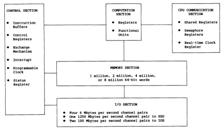
CONTROL SECTION COMPUTATION CPU COMMUNICATION
SECTION SECTION
•
Instruction•
Registers•
Shared RegistersBuffers
•
Functional•
Semaphore•
control Units RegistersRegisters
•
Real-time Clock•
Exchange RegisterMechanism
•
Interrupt•
Programmable MEMORY SECTIONClock
>----1 million, 2 million, 4 million,
•
Status or 8 million 64-bit wordsRegister
I - - - I/O SECTION
•
Four 6 Mbytes per second channel pairs•
One 1250 Mbytes per second channel pair to SSD [image:15.613.87.543.346.610.2]•
Two 100 Mbytes per second channel pairs to lOSFigure 1-2. Basic Organization of the Single-processor System
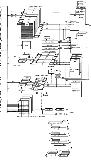
Ak
lAO)
.~ I +1 I
i
~~~~~III~
~---~~~~-.-.
31 Instruction Buffers,=.===;~_..:S.:..J1 I
t
The Vector Pop/ParIty .shares its input path with the Reciprocal Approximation unit
The Second Vector LOQlcal shares its input and output path with the Floatlnq-polnt Multiply unit.
Second Vector Loolcal and Index Generation units are not available on all systems.
Figure 1-3. Control and Datapaths for the CPU
[image:16.612.197.497.75.614.2]INTERFACES
The Cray mainframe is designed for use with front-end computers in a
computer network. A front-end computer system is self-contained and
executes under the control of its own operating system.
Standard interfaces connect the Cray mainframe's 1/0 channels to channels
of front-end computers, providing input data to the Cray and receiving
output from i t for distribution to peripheral equipment. Interfaces
compensate for differences in channel widths, machine word size,
electrical logic levels, and control signals. The front-end computer
system can be connected either to the Master 1/0 Processor (MIOP) of the
lOS or to the mainframe.
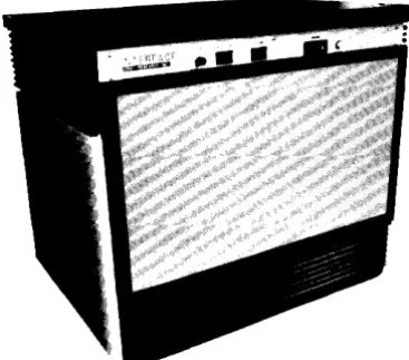
The front-end interface is housed in a stand-alone cabinet (figure 1-4)
located near the host computer. Its operation is invisible to both the
front-end computer user and the Cray user.
A primary goal of the interface is to maximize the use of the front-end
channel connected to the Cray system. Since the MIOP channel connected to
the interface is faster than any front-end channel connected to the
interface, the burst rate of the interface is limited by the maximum rate of the front-end channel.
Interfaces to front-end computers allow the front-end computers to service the Cray mainframe in the following ways:
• As a master operator station
• As a local operator station
• As a local batch entry station
• As a data concentrator for multiplexing several other stations
into a single Cray channel
• As a remote batch entry station
• As an interactive communication station
Peripheral equipment attached to the front-end computer varies depending on the use of the Cray system.
Figure 1-4. Typical Interface Cabinet
I/O SUBSYSTEM
The lOS, shown in figure 1-5, is standard on all CRAY X-MP series
computer systems and has two, three, or four lOPs, a Buffer Memory, and
required interfaces. It is designed for fast data transfer between
front-end computers, peripheral devices, storage devices, and the lOS's Buffer Memory or between its Buffer Memory and the Central Memory of a Cray mainframe.
Four types of lOPs may be configured in an lOS: an MIOP, a Buffer lOP
(BIOP), a Disk lOP (DIOP), and an Auxiliary lOP (XIOP). All lOSs must
have at least one MIOP and one BIOP. The number of DIOPs and XIOPs is
site dependent.
Each lOP 6f the lOS has a memory section, a control section, a
computation section, and an I/O section. I/O sections are independent
and handle some portion of the I/O requirements for the subsystem. Each
lOP also has six direct memory access (DMA) ports to its Local Memory.
The MIOP controls the front-end interfaces and the standard group of
stationt peripherals. The Peripheral Expander interfaces the station
peripherals to one DMA port of the MIOP. The MIOP also connects to
Buffer Memory and to the mainframe over a 6 Mbyte per second channel
pair.
t The term station means both hardware and software. Station is the
link to the front-end system or can act as a limited front-end system (as the MIOP).
[image:18.617.222.406.85.247.2]Figure 1-5. 1/0 Subsystem Chassis
The BIOP is the main link between the mainframe's Central Memory and the
mass storage devices. Data from mass storage is transferred through the
BlOP's Local Memory to the mainframe's Central Memory through a 100 Mbyte per second channel pair.
[image:19.612.206.405.69.475.2]The DIOP is used for additional disk storage units (DSUs). This
processor can handle up to four disk controller units (DCUs).with up to
16 disk storage units. The DIOP uses one DMA port for each controller,
one DMA port to connect to Buffer Memory, and another DMA port to connect a 100 Mbyte per second channel pair to the mainframe Central Memory.
The XlOP is used for block multiplexer channels and interfaces to a
maximum of four BMC-4 Block Multiplexer Controllers. Each controller can
handle up to four block multiplexer channels. The XIOP uses one DMA port
for each controller and another DMA port to connect with Buffer Memory.
lOS hardware allows simultaneous data transfers between the MIOP, BIOP, DIOP, or XIOP of the lOS and the mainframe's Central Memory.t
Section 2 describes the CPU 1/0 section for the Cray System. Refer to
the 1/0 Subsystem Hardware Reference Manual for a complete description of
the lOS.
DISK STORAGE UNITS
For mass storage, the system uses CRI disk storage units. A disk
controller unit interfaces the disk storage units with an lOP of an lOS
through one DMA port. Up to four disk storage units can be connected to
a single disk controller unit.
The lOP and the disk controller unit can transfer data between the DMA port and four disk storage units with all disk storage units operating at
full speed without missing data or skipping revolutions. A m1n1mum of 2
and a maximum of 48 disk storage units can be configured on an lOS. The
lOS chassis houses the disk controller uni~.
Each disk storage unit has two accesses for connecting i t to
controllers. The second independent datapath to each disk storage unit
exists through another CRl controller. Reservation logic provides
controlled access to each disk storage unit. The Cray operating system
COS software does not support dynamic sharing of devices. The Disk
Systems Hardware Reference Manual includes further information about the mass storage subsystem.
t
Software to support the 100 Mbyte per second channel pair to the MIOPand XIOP is not currently available.
SOLID-STATE STORAGE DEVICE
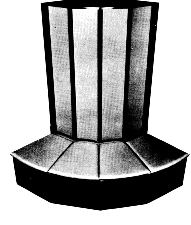
The SSD, shown in figure 1-6, is used for temporary data storage. A
special Cray interface cable, set at a maximum speed of 1250 Mbytes per
second, transfers data between the mainframe's Central Memory and theSSD.
Refer to the SSD Solid-state Storage Device Hardware Reference
Manual for more information about the SSD to mainframe channel connection.
Figure 1-6. Solid-state Storage Device Chassis
CSM0111000
CRAY PROPRIETARY
1-11 [image:21.612.116.497.162.610.2]---,,---CONDENSING UNITS
Condensing units (figure 1-7) contain the major components of the
refrigeration system used to cool the computer chassis and consist of two
25-ton condensers. Heat is removed from the condensing unit by a
second-level cooling system that is not part of the computer system. Freon, which cools the computer, picks up heat and transfers i t to water in the condensing unit.
Figure 1-7. Condensing Unit
POWER DISTRIBUTION UNITS
The Cray mainframe, IDS, and SSD all operate from 400-Hz, three-phase
power.
The mainframe and IDS operate from the same power distribution
unit. This unit contains adjustable transformers for regulating the
voltage to each chassis column.
The power distribution unit also contains temperature and voltage
monitoring equipment that checks temperatures at strategic locations on the chassis columns, and automatic warning and shutdown circuitry to protect the equipment in case of overheating or excessive cooling. Control switches for the motor-generators and the condensing unit are also mounted on the power distribution unit.
A smaller power distribution unit performs similar functions for the SSD chassis.
Figure 1-8 shows the power distribution units for the mainframe and lOS (left) and for the SSD (right).
Figure 1-8. Power Distribution Units
MOTOR-GENERATOR UNITS
Motor-generator units convert primary power from the commercial power
mains to the 400-Hz power used by the system. These units isolate the
system from transients and fluctuations on the commercial power mains. The equipment consists of two or three motor-generator units and a
control cabinet. Figure 1-9 shows a typical motor-generator and its
control cabinet.
Figure 1-9. Motor-generator Equipment
[image:24.613.369.540.174.456.2]SYSTEM CONFIGURATION
Figures 1-10 and 1-11 illustrate two configurations for the CRAY X-MP
single-processor computer systems.
MIOP
BIOP
FRONT -END
COMPUTERS
FRONT-END
INTERFACES
TO MAINFRAME OR I/O SUBSYSTEM
CRAY X-MP MAINFRAME . . . 1.2.4. OR 8 MILLION DIOP
X lOP
- Cray 6 Mbyte channel
. . . . Cray 100 Mbyte channel
. . . . Cray 1250 Mbyte channel
64-B IT WORDS
Figure 1-10. Block Diagram of a Typical CRAY X-MP Single-processor
System with Full Disk Capacity
CSM0111000 CRAY PROPRIETARY
550
>-a:
ffi
PERI PHERAL EXPANDER
MIOP
BIOP
FRONT -END
COMPUTERS
FRONT-END INTERFACES
TO MAINFRAI4E OR I/O SUBSYSTEM
~ ~---1 CRAY X - MP MAINFRAME
~
,.
... ..
: : . . I, 2,4, OR 8 MILLION
~ DIOP 64-8 IT WORDS
)( lOP
1 TO 4
BLOCK MULTIPLEXER - - 1 TO 16 CHANNELS CONTROLLERS
- Cray 6 Mbyte channel
_ Cray 100 Mbyte channel
- Cray 1250 Mbyte channel
Figure 1-11. Block Diagram of a Typical CRAY X-MP Single-processor
System with Block Multiplexer Channels
SSD
[image:26.612.81.538.60.373.2]CPU RESOURCES
The Central Processing Unit (CPU) has access to the mainframe's Central
Memory, the inter-CPU communication section, and the liD section. The
following pages describe these areas.
CENTRAL MEMORY
Central Memory consists of a number of banks of solid-state,
random-access memory (RAM) that is shared by the CPU and the I/O
2
section. Four Central Memory sizes are available with either 16K- or
64K-chip technology: 1 or 2 million words in 16 banks (16K), 4 million
words in 32 banks (16K), 4 million words in 16 banks (64K), and 8 million
words in 32 banks (64K). Banks are independent of each other;
sequentially addressed words reside in sequential banks. Each word is 72
bits with 64 data bits and 8 check bits.
Central Memory cycle time takes 8 clock periods (CPs) to execute. Access
time, the time required to fetch an operand from Central Memory to an operating register, is 17 CPs for address (A) and scalar (S) registers.
Access time is 20 CPs plus vector length for a vector (V) register and
19 CPs plus block length for a block transfer to a intermediate address
(B) or intermediate scalar (T) register.
The maximum transfer rate for B, T, and V registers is 3 words per CP;
for A and S registers, i t is 1 word every 2 CPs. Transfer of
instructions to instruction buffers occurs at a rate of 32 parcels
(8 words) per CPo For the liD section, the transfer rate is 2 words per
CPo
Central Memory features are summarized below and are described in detail in the following paragraphs.
• 1, 2, 4, or 8 million words of integrated circuit memory
• 64 data bits and 8 error-correction bits per word
• 16 or 32 interleaved banks
• 8-CP bank cycle time
• Single-error-correction/double-error-detection (SECDED)
• 3 words per CP transfer rate to B, T, and V registers
• 1 word per 2-CP transfer rate to A and S registers
• 8 words per CP transfer rate to instruction buffers
• 2 words per CP transfer rate to I/O concurrent with all memory
activity except instruction fetch and exchange
MEMORY ORGANIZATION
Memory is organized to provide fast, efficient access for the CPU. Data
transfers to and from memory are corrected with SECDED. Central Memory
is organized into four sections with 4 or 8 banks in each section. The
16-bank phasing is standard for a 1- or 2-million-word system (16K) and 4-million-word system (64K); 32-bank phasing is standard for a
4-million-word system (16K) and a 8-million-word system (64K).
As shown in figure 2-1, the CPU has an independent access path into each
of the four memory sections. For 1/0 and instruction fetch operations,
an additional access path into each section of memory is provided (dashed
lines in figure 2-1). These additional access paths allow instruction
fetches to proceed at 8 words per CP and 1/0 to reference 2 words per CPo
SECTION 0
Banks 0,4,10,14,t 20,24,30,34
SECTION 1
Banks 1,5,11,15,t 21,25,31,35
A
CPU
Ports
B C
Upper
CPU Path Selection
CPU Path Selection
SECTION 2
Banks 2,6,12,16,t 22,26,32,36
SECTION 3
Banks 3,7,13,17,t 23,27,33,37
Figure 2-1. Central Memory Organization for a
Single-processor System
t
Low-numbered 4 banks in each section are in a 16-bank system.MEMORY ADDRESSING
Memory addressing is dependent on system memory architecture (chip size
and number of banks) and memory size. The following paragraphs describe
the memory addressing for the different configurations of the single-processor system.
Memory addressing for 16-bank, 16K-chip, 1- and 2-million-word system
A word in a 16-bank, 16K-chip memory is addressed in a maximum of 21 bits,
as shown in table 2-1. The low-order 4 bits specify one of the 16 banks.
The next 14-bit field specifies an address within the chip. The
high-order 3 bits specify one chip on a module.t
Memory addressing for 32-bank, 16K-chip, 4-million-word system
A word in a 32-bank, 16K-chip memory is addressed in a maximum of 22 bits,
as shown tn table 2-1. The low-order 5 bits specify one of the 32 banks.
The next 14-bit field specifies an address within the chip. The
high-order 3 bits specify one chip on the module.
Memory addressing for 16-bank, 64K-chip, 4-million-word system
A word in a 16-bank, 64K-chip memory is addressed in a maximum of 22 bits,
as shown in table 2-1. The low-order 4 bits specify one of the 16 banks.
The next 16-bit field specifies an address within the chip. The
high-order 2 bits specify one chip on the module. t
Memory addressing for 32-bank, 64K-chip, 8-million-word system
A word in a 32-bank, 64K-chip memory is addressed in a maximum of 23 bits,
as shown in table 2-1. The low-order 5 bits specify one of the 32 banks.
The next 16-bit field specifies an address within the chip. The
high-order 2 bits specify one chip on the module.
t Hardware assembles the address using a 4-bit bank field. The
software, when assembling the address for memory error correction,
receives 5 significant bits from the Exchange Package. The high-order
bit (bit 4 counting right to left from 0) must be discarded by the
software when assembling the address for memory error correction.
Table 2-1. Memory Addressing Formats
Chip Memory No. of No. of
Type Size Banks Columns Address Format
16K 1 or 2 16 6
220 217 2 3 2°
Chip Internal bit 4-bit
address address in bank
select chip
16K 4 32 6
221 2 18 24 2°
Chip Internal bit 5-bit
address address in bank
select chip
64K 4 16 6
221 2 19 2 3 20
Chip Internal bit 4-bit
address address in bank
select chip
64K 8 32 6
222 220 24 2°
Chip Internal bit 5-bit
address address in bank
select chip
[image:30.612.91.536.71.524.2]MEMORY ACCESS
The CPU has five memory access ports: Port A, Port B, Port C, and two
1/0 ports. Each port is capable of making one reference per CPo Both
1/0 ports can be active simultaneously. Ports A, B, and C are used for
CPU register transfers. B, T, and vector memory instructions issue to a
particular memory port:
• Vector read (block reads only), and B read instructions (176,
034) use Port A
• Vector read (block reads only), and T read instructions (176,
036) use Port B
• Vector store, B, or T store instructions (177, 035, and 037)
and scalar instructions (100 through 137) use Port C
Once an instruction issues to a port, that port is reserved until all references are made for that instruction.
The references for each element of a block transfer (V, B, or T) are made
and completed in sequence through a port. Since each reference is
examined individually for possible conflicts, the data flow for a
transfer may not be continuous. If an instruction requires a port that
is busy, issue is blocked. Total execution time of the transfer depends
on the number and type of conflicts encountered during the transfer.
NOTE
Because concurrent block reads and writes are not
examined for memory overlap hazard conditions (that is,
read before write or write before read), the software must detect where this condition occurs and ensure sequential operation.
The bidirectional memory mode enable (002600), bidirectional memory mode
disable (002500), and the complete memory reference (002700) instructions
are provided to resolve these cases and assure sequential operation. If
the bidirectional memory mode is clear, block reads and writes are not
allowed to operate concurrently. Instruction 0027 allows the program to
wait until the last references of all preceding block transfers are past the conflict resolution stage and the transferred data is being
transmitted to the designated memory or register locations. Instruction
0027 provides software a mechanism, wherever necessary in the program, to guarantee sequential memory operation.
Issue of scalar memory references requires Ports A, B, and C to be available, ensuring sequential operation between block transfers and scalar references.
A scalar reference conflict is detected in CP 3 of execution. If a
conflict occurs, one more scalar reference is allowed to issue. A third
scalar reference holds issue if the conflict condition still exists for the preceding scalar reference.
Scalar references always execute in the order they are issued.
Instruction 0027 detects when all scalar references are past the conflict resolution stage within the CPU.
One-half of the liD channels reference memory through each of the liD
ports. The liD ports can be active regardless of the activities on Ports
A, B, or C.
When an instruction fetch request occurs, all referencing from the eight memory ports is inhibited (in this regard, the CRAY X-MP single-processor
system is like the CRAY X-MP dual-processor system). When memory is
quiet, the fetch proceeds and references 32 banks in the next 4 CPs (10
CPs if 16 banks). Then nonfetch referencing from the ports is enabled.
NOTE
A fetch sequence that follows a scalar store can, under
certain conditions, complete before the store. For
this to happen, however, an out-of-buffer condition must arise before the scalar store is in CP 2 of
execution. The out-of-buffer condition can occur
before the scalar store is in CP 2 of execution if a buffer boundary is crossed without doing a branch. This presents a problem only if the fetch and store are
to the same area in memory. Therefore, software that
uses dynamic coding should ensure that the code generated is actually in memory before that area of memory is fetched into the instruction buffers.
An exchange requires all activities within the CPU to complete before the exchange request is made.
When the exchange request is made, all referencing from the memory ports
is inhibited. When memory is quiet, the exchange proceeds and references
16 banks in the next 25 CPs. Each bank is referenced twice during this
time, once for a read and once for a write. A fetch request follows
immediately after the exchange reference is complete and then referencing from the memory ports is enabled.
Conflict resolution
During each CP, references to the memory ports in the system are examined
for memory access conflicts. If a conflict occurs for a reference, the
reference is held and no further referencing from that port is allowed until the conflict is resolved.
Two types of memory access conflicts can occur; Bank Busy and Section
Access.
Bank Busy conflict - The Bank Busy conflict is caused by any port
requesting a bank currently in a reference cycle. Resolution of this
conflict occurs when the bank cycle is complete. Hold reference because
of a Bank Busy conflict, 1 to 7 CPs.
Section Access conflict - The Section Access conflict is caused by two or more ports in the CPU requesting any bank in the same section.
Resolution of this conflict is based on priority and the Bank Busy
conflict. The highest priority port with no Bank Busy conflict is
allowed to proceed, all other ports involved in this conflict hold (refer
to Memory access priorities subsection). Hold reference 1 CP because of
a section access conflict.
Memory access priorities
The following statements are used to resolve memory access conflicts and determine the priority between Ports A, B, and C:
• Any port with an odd increment always has a higher priority than a
port with an even increment regardless of their issued sequence.
• Among all ports with the same type of increment (odd or even), the
relative time of issue determines the priority, with the first issued having the highest priority.
• 1/0 ports are always lowest priority.
16-BANK PHASING
The effect of 16-bank phasing on instruction fetches is a predictable
increase of 6 CPs for filling instruction buffers. Otherwise, the amount
of performance degradation for 16 banks instead of 32 banks is not
readily predictable since i t largely results from an increased number of memory conflicts.
For maintenance purposes, a 32-bank system can be modified to operate with only 16 banks and use either the lower or upper half of memory. Maintenance is accomplished by setting the bank select switch on the mainframe's control panel to the lower or upper banks.
MEMORY ERROR CORRECTION
A SECDED network is used between the CPU and memory. SECDED assures that
data written into memory can be returned to the CPU with consistent precision (figure 2-2).
If a single bit of a data word is altered, the single error alteration is
automatically corrected before passing the data word to the computer. If
2 bits of the same data word are altered, the error is detected but not
corrected. In either case, the CPU can be interrupted, depending on
interrupt options selected to allow processing of the error. For 3 or
more bits in error, results are ambiguous.
o
'" '"
..
-
Data Fanin Error-
CPUCorrect
Data Memory
Bits
63
~
Error
..
Detect-r
CheckBits 71
Figure 2-2. Memory Datapath with SECDED
The SECDED error processing scheme is based on error detection and
correction codes devised by R. W. Hamming.t An 8-bit check byte is
appended to the 64-bit data word before the data is written in memory. The 8 check bits are generated as even parity bits for a specific group
of data bits. Figure 2-3 shows the bits of the data word used to
determine the state of each check bit. An X in the horizontal row
indicates that data bit contributes to the generation of that check bit. Thus, check bit 0 is the bit that makes group parity even for the group of bits 21, 2 3 , 2 5 , 27, 2 9 , 211, 213 , 2 15 , 217, 219 , 221, 223, 225, 227, 2 29 , and 2 31 through 255.
t
Hamming, R.W., "Error Detection and Correcting Codes", Bell SystemTechnical Journal, 29, No.2, pp. 147-160 (April, 1950).
check bit 0 check bit 1
check bi t
check bit 3
check bit 4 check bi t 5
CHECK BYTE
x
x
x
check bi t 6
check bi t 7 x
y.
x x x x x x x x x x x x x x x x x x x x x x x x
x x x x
x x x x x x x x
x x x x
x x x
x x x x
x x x x
x x x x
x x x x x x x x x x x x x x x x x x x x x x x x
Figure 2-3.
x x x x x x x x
x
x x x x x x x x x x x x x x x x
x x x x x x x
x x x x x x x x
x x x x
x x x x x x x x
x x x x x x
x x x x x x x x x x x x
x x x x x x x x x x x x x x x x x x x x x x x
x x x x
x x x x
x x x x x x x x x x x x x x x x x x x x x x x x x x x x x x x x x x x x
x x x x
x x x x x x x x
x x x x x x x x
x x x x x x x x
x x x x x x x x x x x x x x x x x x x x x x x x x x x x x x x x x x x x x x x x x x x x x x x x
Error Correction Matrix
The 8 check bits and the data word are stored in memory at the same
location. When read from memory, the same 64-bit matrix of figure 2-3 is
used to generate a new set of check bits, which are compared with the old
check bits. The resulting 8 comparison bits are called syndromet bits
(S bits). The states of these S bits are all symptoms of any error that
occurred (1=No compare). If all syndrome bits are 0, no memory error is
assumed.
Any change of state of a single bit in memory causes an odd number of
syndrome bits to be set to 1. A double error (an error in 2 bits)
appears as an even number of syndrome bits set to 1.
t Syndrome: Any set of characteristics regarded as identifying a
certain type, condition, and so on. (Webster's New World Dictionary).
CSM0111000 CRAY PROPRIETARY 2-9
[image:35.613.85.540.71.464.2]The matrix is designed so that:
• If all S bits are 0, no error is assumed.
• If only 1 S bit is 1, the associated check bit is in error.
• If more than 1 S bit is 1 and the parity of S bits SO through S7
is even, a double error (or an even number of bit errors) occurred within the data bits or check bits.
• If more than 1 S bit is 1 and the parity of all S bits is odd, a
single and correctable error is assumed to have occurred. The
syndrome bits can be decoded to identify the bit in error.
• If 3 or more memory bits are in error, the parity of all S bits is
odd and results are ambiguous.
Modules involved with generating and interpreting the 8-bit check byte used for SECDED include logic that can be used for verifying check bit
storage, check bit generation, and error detection and correction. Refer
to appendix D for information on SECDED maintenance functions.
INTER-CPU COMMUNICATION SECTION
The inter-CPU communication section of the mainframe contains special
hardware for data storage, control, and for a Real-time Clock (RTC). The
RTC, Shared Address (S8), Shared Scalar (ST), and Semaphore (SM) registers
are available for use by the CPU. These registers, with their sources and
destinations, are shown in figure 2-4 and d~scribed in the following
paragraphs.
REAL-TIME CLOCK
The mainframe contains one RTC register. Programs can be timed precisely
by using the CP counter. This counter is 64 bits and advances one count
each CPo Since the clock advances synchronously with program execution,
i t can be used to time the program to an exact number of CPs. In such an
application, however, the counting can contain counts from other tasks if an interrupt occurs before the end time is read.
Instructions used with the RTC register are:
2-10
Octal Code
0014jO 072iOO
CAL Syntax
RT Sj
si
RTDescription
Enter the RTC register with (Sj)
Transmit (RTC) to
Si
Sj
---11
RTCSi .. :
Si
STj ~--~~~...L___.
Figure 2-4. Shared Registers and Real-time Clock
In monitor mode, a program reads the CP counter by using instruction 072
and resets i t with instruction 0014jO.
INTER-CPU COMMUNICATION AND CONTROL
Three sets of shared registers can be used by the CPU for storage and
control. Each set contains eight 24-bit SB registers, eight 64-bit ST
registers, and 32 1-bit SM registers.
The CPU's Cluster Number (CLN) register determines which set of shared
registers is accessed by the CPU (clustering). The CLN register is
loaded from the Exchange Package or if the CPU is in monitor mode,
through instruction 0014j3.
[image:37.612.199.423.73.396.2]The CLN register can contain one of four different values. Values 1, 2, or 3 allow the CPU to access one of the three sets of shared registers.
Value 0 prevents any access to shared registers by the CPU. If the value
is 0, instructions regarding the shared registers become no-ops, except
for the instructions returning values to Ai or
Si,
which return azero value.
Shared Address and Shared Scalar registers
The Shared Address (SB) and Shared Scalar (ST) registers require no
hardware reservations. Instructions used with the SB and ST registers
are:
Octal Code CAL Syntax Description
026ij7
AiSBj
Transmit(SBj)
to Ai027ij7
SBj
Ai Transmit (Ai) toSBj
072ij3
siSTj
Transmit(STj)
to si073ij3
STj Si
Transmit(Si)
toSTj
Semaphore registers
The SM registers can be used by the CPU for storage and control. The
test and set instruction first tests the value of the selected SM
~~ister. If the value is 0, the instruction issues and sets that SM
register to a 1. If the value is 1, the instruction holds issue until
the value is
o.
If the CPU holds issue on a test and set instruction, i t receives a
deadlock interrupt. No deadlock interrupt can occur in cluster 0 (CLN=O).
When an interrupt occurs, normally the instructions already in the Next
Instruction Parcel (NIP) and Current Instructio~ Parcel (CIP) registers
are allowed to issue before the exchange sequence starts. If a test and
set instruction is holding in the CIP register and an interrupt occurs, a
special exchange startup sequence is initiated. Here, the instruction in
the NIP register and the test and set instruction in the CIP register are discarded and the Program Counter {P} register is adjusted to point to
the discarded test and set instruction. The Waiting on Semaphore (WS)
flag in the Exchange Package sets, indicating a test and set instruction
was holding in the CIP register when the interrupt occurred. The
exchange sequence is then started.
Instructions used with the SM registers are:
2-12
Octal Code
0034jk
0036jk
CAL Syntax
SMjk
SMjk
1,TS
o
Description
Test and set,
SMjk
Clear
SMjk
Octal Code CAL Syntax Description
0037jk SMjk 1 Set SMjk
072i02
Si
SM
Transmit(SM)
toSi
073i02 SM Si Transmit (Si) to SM
CPU INPUT/OUTPUT SECTION (Maximum Configuration)
The mainframe supports channels connecting i t to the lOS, the optional
SSD, and front-end interfaces. The lOS channel operates at 100 Mbytes
per second, the SSD channel operates at 1250 Mbyte per second, and the front-end interface channels operate at 6 Mbytes per second.
One 1250 Mbyte per second channel pair is used to transfer data between
Central Memory and the SSD. These channels are 128 bits wide and use
16 check bits in each direction. A maximum transfer rate of over
10 gigabits/s is possible on the channel. The channel is two parallel
64-bit channels, each with SECDED; therefore, under certain circumstances the full-width channel can correct double errors.
Two 100 Mbyte per second channel pairs transfer data between Central
Memory and an lOS. A 100 Mbyte per second channel is 64 bits wide and
uses 8 check bits in each direction. Data words are transferred in
blocks of 16 under control of Data Ready and Data Transmit control
signals. Each 100 Mbyte per second channel has a maximum transfer rate
of approximately 850 Mbits per second.
lOS communication with the CPUs is over four pairs of control channels,
each with a maximum transfer rate of 6 Mbytes per second. Each 6 Mbyte
per second channel is 16 bits wide.
There are two 1/0 ports. The channels are hardwired into a port with two
6 Mbyte per second channel pairs, one 100 Mbyte per second channel pair,
and one-half of the SSD's 1250 Mbyte per second channel per port. Each
port can transfer data at a rate of 1 word per CPo For the 100 Mbyte per
second channels and one-half of the 1250 Mbyte per second channels, each time a buffer makes a reference, i t holds the port until complete,
usually 16 words.
All 1/0 uses the 1/0 ports to memory, and a scanner controls access to
these ports. All CPU memory ports (Ports A, B, and C) have higher
priority than the 1/0 ports.
Channel features of the 1/0 section are summarized below and described in the remainder of this section.
• One channel pair with a 1250 Mbytes per second maximum transfer
rate per channel; 128 data bits and 16 check bits in each direction.
• Two channel pairs with a 100 Mbytes per second maximum
transfer rate per channel; 64 data bits, 3 control bits, and 8 check bits in each direction.
• Four IIO channel pairs with a 6 Mbytes per second maximum
transfer rate per channel
•
•
•
16 data bits, 3 control bits, and 4 parity bits in each direction
Lost data detection
Channels are divided into groups, each group contains either input or output channels
Channel groups are served equally by memory (each group is scanned every 4 CPs)
Channel priority resolved within channel groups
DATA TRANSFER FOR SOLID-STATE STORAGE DEVICE
Data is transferred directly between the SSD and the mainframe using 1250
Mbyte per second channels. This 1250 Mbyte per second channel is
128 bits wide and is programmed through software. The Solid-state
Storage Device (SSD®) Reference Manual describes programming details for the SSD.
DATA TRANSFER FOR IIO SUBSYSTEM
A 100 Mbyte per second channel pair transfers data between Central Memory
of the mainframe and the lOP. Each channel is 64 bits wide and handles
data at approximately 100 Mbytes per second. Each channel uses an
additional 8 check bits for SECDED, as is used in Central Memory.
The CPU side of a 100 Mbyte per second channel pair uses a pair of
16-word buffers to stream the data out of Central Memory and another pair
to stream data into Central Memory. On output, as one buffer block is
being sent to the lOP, the other buffer is filling from Central Memory. Similarly, on input, one buffer block is filling from an lOP while the other is transmitting to Central Memory.
At the lOP side of a 100 Mbyte per second channel pair, data passing into Local Memory (an lOP's memory) is double-buffered and disassembled into
16-bit parcels. The channel side passing data from Local Memory simply
assembles 16-bit parcels into 64-bit words for transmission to a CPU.
An lOP controls a 100 Mbyte per second channel pair linking i t with
Central Memory. The lOP initiates all data transfers on the channel and
performs all error processing required for the channel. There are no CPU
instructions for the 100 Mbyte per second channel pair. The I/O
Subsystem Hardware Reference Manual for your lOS contains programming details for the 100 Mbyte per second channel pair.
6 MBYTE PER SECOND CHANNELS
Standard control channels for the system are 6 Mbyte per second
channels. Each 6 Mbyte per second channel has 16-bit asynchronous
control logic used for front-end interfaces. The instructions used with
6 Mbyte per second channels follow.
Octal Code CAL Syntax
0010jk CA,Aj Ak
0011jk CL,Aj Ak
0012jk CI,Aj
033iOO Ai CI
033ijO Ai CA,Aj
033ij1 Ai CE,Aj
Description
Set the Current Address (CA) register
for the channel indicated by (Aj) to
(Ak) and activate the channel
Set the Limit Address (CL) register for
the channel indicated by (Aj) to
(Ak)
Clear the Interrupt flag and Error flag
for the channel indicated by (Aj):
Output channel k=O; clear MC, k=l; set
MC. Input channel k=O; no operation,
k=l; clear held ready.
Transmit channel number to Ai
Transmit address of channel (Aj) to Ai
Transmit Error flag of channel (Aj)
to Ai
6 MBYTE PER SECOND CHANNEL OPERATION
Each input or each output channel directly accesses Central Memory. Input channels store external data in memory and output channels read
data from memory. A primary task of a channel is to convert 64-bit
Central Memory words into 16-bit parcels or 16-bit parcels into 64-bit
Central Memory words. Four parcels make up one Central Memory word with