LOW NOISE LOW POWER TRANSIMPEDANCE AMPLIFIER
IN 0.18µM CMOS TECHNOLOGY
MOHAMMAD ARIF SOBHAN BHUIYAN, KALAIVANI A. TARUMARAJA, MAMUN BIN IBNE REAZ, FAZIDA HANIM HASHIM, SAWAL HAMID MD. ALI
Department of Electrical, Electronic and Systems Engineering, University Kebangsaan Malaysia,
43600, Bangi, Selangor, Malaysia E-mail: [email protected]
ABSTRACT
Low noise and low Power transimpedance amplifiers (TIA) are essential modules for optical sensor based systems. But low power and low noise TIAs are still a challenge for the scientists despite of rapid advances in complementary metal oxide semiconductor (CMOS) technology. This paper proposes a three-stage nested miller compensated (NMC) based design of low noise low power transimpedance amplifier for stable wideband operation. The circuit is designed in the 0.18µm CMOS technology by using Mentor Graphics environment. The simulation results show that the proposed TIA can operate at frequency 20 KHz and produces an output of 1.4265V for ±1.2 V input voltages dissipating only 2.9206 mW power at 27°C temperature. The complete layout of the TIA is only 0.005 µ m2.This shunt-feedback TIA can be a better choice for high-resolution, low-to mid frequency applications.
Keywords: CMOS, low power, Opamp, TIA
1. INTRODUCTION
The current trend of all modern devices is to make it small, portable and cost-effective [1-5]. As a result the level of integration in all concurrent devices such as RFID, Bluetooth, Zigbee, Wi-Fi etc. has rapidly been increased, in last few years, due to the considerable advancement of CMOS technology [6-12]. Therefore, the prospect for integration of RF/digital/analogue circuits on a single chip becomes feasible and economical. As a result both individual and industry are becoming benefited [13-15].
A transimpedance amplifier (TIA) is a voltage amplifier that converts the current into a voltage. It is commonly used as shunt feedback path [16]. The ideal input has zero impedance, and the input signal is current. An output has low output impedance. Transimpedance amplifiers are commonly used in receivers for optical sensor based communication devices specially in preamplifier circuits [17]. The current generated by a photodetector causes a photo voltage in a nonlinear fashion and therefore, the amplifier has to prevent any large voltage by its low input impedance and generate either a 50 Ohm signal to drive a coaxial cable or a voltage signal for further amplification. Several fundamental structures of such amplifiers are available for different kinds of applications. The amplifiers have gained
preponderance over other linear amplifiers for low power and low voltage applications [18]. A low noise operational amplifier is suppose to have application oriented optimized performance [19].
Design of a high performance transimpedance amplifier is still a challenge for the sensor designers. For sensors that uses shunt feedback photo detectors should have a low noise, low power, high gain, fast settling and wide bandwidth amplifier [20, 21]. To achieve a best trade-off among these parameters, different researchers proposed several design compensation [20, 22-24]. The basic shunt-feedback topology uses a voltage amplifier with a feedback network that has the potential of obtaining lower overall input referred noise by optimizing the transistor sizes and aspect ratios in the amplifier’s input stage [16].
This paper proposes low power design of a three stage Nested Miller compensation based transimpedance amplifier for the applications where low noise and stable wide band operation is the requirements. The circuit is designed in the 0.18µm CMOS technology by using Mentor Graphics environment. The simulation results confirm that the proposed TIA can be the best choice for low power optical sensor based communication receivers.
2. SHUNT-FEEDBACK TOPOLOGY
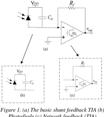
The basic shunt feedback topology, as shown in figure 1, usually uses a feedback loop network with the voltage amplifier to achieve wide band tuning. Such a structure can degrade the noise performance and it leads to a balance between sensitivity and bandwidth. It also reduces the DC voltage gain of the circuit. In the case of shunt feedback TIA, as an alternative, using the voltage gain control (CVG) and bootstrapping circuits are recommended to improve the bandwidth and to eliminate the signal swing from the photodiode. In addition, it also allows CVG shunt feedback TIA to handle the signal with soft edges and sharp transitions without affecting the transimpedance bandwidth.
Figure 1. (a) The basic shunt feedback TIA (b) Photodiode (c) Network feedback (TIA)
3. NMC VOLTAGE AMPLIFIER OF THREE
STAGE
[image:2.612.312.521.69.252.2]In this paper, a three stage NMC based feedback network for shunt-feedback TIA is proposed. The schematic of the three-stage NMC based amplifier is shown in Fig. 2. The voltage amplifier is made up of two complementary differential gain stages (M1−M5 and M6−M9) and a final common-source gain stage (M10−M11). The compensation network includes, other than capacitors Cc1 and Cc2, a single nulling resistor Rc to eliminate the right-half-plane (RHP) zero. The NMC amplifier design approach is based on the design procedures used in [25] and [26]. The additional circuit design techniques are summarized in the subsequent paragraphs.
Figure 2. Schematic of three-stage NMC amplifier[25][26]
To maximize the slew rate (SR) and gain bandwidth, a p-channel input pair is required at the input stage to compensate the output noise caused by flicker noise. But the main problem is the increase in thermal noise because of less carrier mobility of p-channel transistors compared to their n-channel counterparts. Maximizing the bias current can help to overcome this drawback where input pair (M3, M4) maintains high aspect ratio and large sizes.
The output of the first differential amplifier connected to the gate M10 improves SR performance by providing a pseudo class AB output stage. As a result, output stage has much higher current when it drives a load capacitor than the current flowing through the output with no load. Compensation network is made up of a nulling resistor Rc. At higher frequencies, this compensation network moves the RHP to zero by achieving stability with minimum values of compensation capacitors (Cc1 and Cc2) with NMC amplifier.
Figure 3. Schematic of proposed three-stage NMC amplifier
[image:2.612.110.278.285.473.2] [image:2.612.314.524.521.650.2](M1-M5) and (M6-M9) and final common-source gain stage (M10-M11). However, other compensation networks including Rc, Cc1 & Cc2 in are omitted for the proposed design. The aspect ratios of the width and length of the transistor are shown in Table 1.
Table 1: Transistors Ratio W/L (µm).
Transistor Aspect Ratio (µm)
M1, M2 0.5 / 0.18
M3, M4 0.6 / 0.18
M5 0.65 / 0.18
M6. M7 1.4 / 0.18
M8, M9 0.65 / 0.18
M10 22.5 / 0.18
M11 12.5 / 0.18
While the input noise components of the basic shunt-feedback TIA originate mainly from the thermal noise of feedback resistor, Rf, and the input referred noise of the voltage amplifier. At low frequencies, the input noise is dominated by the feedback resistor’s thermal noise. But at higher frequencies and for sufficiently high loop gain A0, the input referred noise of the voltage amplifier may become dominant [16]. In the proposed TIA, the input noise and the bandwidth are dependent on the feedback resistor Rf. For applications like Photodiode based sensors, large TIA gain is required. While increasing the value of Rf can cause a decrease in the input noise contribution and an increase in the TIA transimpedance gain.
4. RESULTS AND DISCUSSIONS
The proposed TIA has been designed in 0.18 µm CMOS process using the Mentor Graphics software environment. The properties of input and output voltages used in the simulation are described in table 2. The simulation result of three stage NMC voltage amplifier is shown in Fig. 4. Both the input voltages V (inA) and V (inB) of the amplifier are ±1.2 V and the output is 1.4265V. Total power dissipation is 2.9206 mW. The operational frequency of TIA is 20 KHz.
Table 2: Characteristics of input and output voltages.
Parameter NMC Amplifier
Voltage(V) V(inA/inB) V(out)
Pulse width (µs) 21.000 20.855
Risetime (ns) 800 799.97
Settle Time (µs) 72.950 72.938
Fall time (ns) 800 792.36
Maximum Voltage(V)
±1.2 1.4265
[image:3.612.311.526.45.242.2]Voltage(V) V(inA/inB) V(out)
Figure 4. Input and output waveforms of TIA
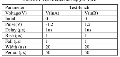
[image:3.612.316.520.368.466.2]It should be noted that in case of soft-edged waveforms, the first operating mode of the TIA is preferred to reduce the DC and lower frequency components. On the other hand, in the case of sharp-edged waveforms, the second operating mode of the TIA is required for its appropriate function. The test bench set up for proposed TIA is given in table 3.
Table 3: Test bench set up for TIA.
Parameter TestBench
Voltage(V) V(inA) V(inB)
Intial 0 0
Pulse(V) -1.2 1.2
Delay (µs) 1us 1us
Rise (µs) 1 1
Fall (µs) 1 1
Width (µs) 20 20
Period (µs) 50 50
RMS Noise performance of the proposed TIA is shown in figure 5. Information of RMS noise value describe in table 4.
Figure 5. RMS Noise of Output
Table 4: RMS Noise measurement data.
Noise RMS
Maximum 1.3619m
Peak to Peak 1.3619m
Average 431.22µ
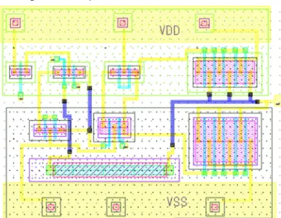
Complete layout of the proposed TIA is shown in figure 6. IC design tools of mentor graphics is used to design the layout. Total size of the chip is 0.005 µm2.
Figure 6. Complete layout of the proposed TIA
5. CONCLUSION
In an optical sensor based communication device, a high-performance transimpedance amplifier is an essential module. In this paper, a three stage operational amplifiers have been designed in 0.18µm CMOS process technology based on NMC technique to improve the power and noise performances. Total power dissipation is 2.9206 mW at input voltages of ±1.2 V which is very low. The total dimension of the proposed TIA is only 0.005 µ m2. Such an amplifier will be the best choice for low power, low noise low-to mid frequency SOC applications.
REFRENCES:
[1] W. M. Kader, H. Rashid, M. Mamun, and M. A. S. Bhuiyan, "Advancement of CMOS Schmitt Trigger Circuits," Modern Applied
Science, vol. 6, pp. 51-56, 2012.
[2] S. S. B. M. Sallah, H. Mohamed, M. Mamun, and M. S. Amin, "Cmos Downsizing: Present, Past And Future," Journal of Applied Sciences
Research, vol. 8, pp. 4138-4146, 2012.
[3] F. B. Arith, M. Mamun, M. A. S. Bhuiyan, and A. A. A. Bakar, "Low Voltage Schmitt Trigger In 0.18 µm CMOS Technology," Advances in
Natural and Applied Sciences, vol. 7, pp.
33-38, 2013.
[4] N. B. Romli, M. Mamun, M. A. S. Bhuiyan, and H. Husain, "Design of a Low Power Dissipation and Low Input Voltage Range Level Shifter in Cedec 0.18-µ m Cmos
Process," World Applied Sciences Journal, vol. 19, pp. 1140-1148, 2012.
[5] M. J. Uddin, A. N. Nordin, M. Reaz, and M. A. S. Bhuiyan, "A CMOS power splitter for 2, 45 GHz ISM band RFID reader in 0, 18 µ m CMOS technology," Tehnički vjesnik, vol. 20,
pp. 125-129, 2013.
[6] K. A. Rosli, M. Mamun, M. A. S. Bhuiyan, and H. Husain, "A Low Loss Wide Swing Cascode Current Mirror in 0.18-µm CMOS Technology,” Journal of Applied Sciences Research, vol. 8, pp. 4096-4102, 2012.
[7] M. B. I. Reaz, M. Islam, M. Sulaiman, M. Ali, H. Sarwar, and S. Rafique, "FPGA realization of multipurpose FIR filter," Proceeding of 4th
International Conference on Parallel and Distributed Computing, Applications and Technologies- 2003, 2003, pp. 912-915.
[8] F. M. Yasin, M. K. Khaw, and M. B. I. Reaz, "Techniques of RFID systems: Architectures and applications," Microwave Journal, vol. 49, pp. 62-74, 2006.
[9] L. F. Rahman, M. B. I. Reaz, M. A. Mohd. Ali, and M. Kamada, "Design of an EEPROM in RFID tag: Employing mapped EPC and IPv6 address," Proceeding of IEEE Asia Pacific Conference on Circuits and Systems, 2010, pp.
168-171.
[10] F. I. B. A. Aziz, M. Mamun, M. A. S. Bhuiyan, and A. A. A. Bakar, "A Low Drop-Out Voltage Regulator in 0.18 µ m CMOS Technology,"
Modern Applied Science, vol. 7, p. p70, 2013.
[11] F. M. Yasin, M. K. Khaw and M. B. I. Reaz, "Radio frequency identification: Evolution of transponder circuit design," Microwave Journal, vol. 49, pp. 56-70, 2006.
[12] J. Uddin, M. B. I. Reaz, M. A. Hasan, A. N. Nordin, M. I. Ibrahimy, and M. A. M. Ali, "UHF RFID antenna architectures and applications," Scientific Research and Essays, vol. 5, pp. 1033-1051, 2010.
[13] K. A. Rosli, R. M. N. H. R. Daud, M. Mamun, and M. A. S. Bhuiyan, "A Comparative Study on SOI MOSFETs for Low Power Applications," Research Journal of Applied
Sciences, Engineering and Technology, vol. 5,
pp. 2586-2591, 2013..
[14] J. Jalil, M. Bin Ibne Reaz, and M. A. M. Ali, "CMOS Differential Ring Oscillators: Review of the Performance of CMOS ROs in Communication Systems," IEEE Microwave
Magazine, vol. 14, pp. 97-109, 2013.
Clock Frequency Divider," Australian Journal
of Basic and Applied Sciences, vol. 6, pp.
73-79, 2012.
[16] A. Trabelsi and M. Boukadoum, "A Comparison of Two CMOS Front-End Transimpedance Amplifiers for Optical Biosensors," 2013.
[17] C. Jung, M. H. Izadi, M. L. La Haye, G. H. Chapman, and K. S. Karim, "Noise analysis of fault tolerant active pixel sensors," in 20th
IEEE International Symposium on Defect and Fault Tolerance in VLSI Systems, 2005, pp.
140-148.
[18] Y. Nemirovsky, I. Brouk, and C. G. Jakobson, "1/f noise in CMOS transistors for analog applications," IEEE Transactions on Electron
Devices, vol. 48, pp. 921-927, 2001.
[19] L. Zhiyuan, Y. Yizheng, and M. Jianguo, "Design procedure for optimizing CMOS low noise operational amplifiers," Journal of
Semiconductors, vol. 30, p. 045005, 2009.
[20] A. Trabelsi, M. Boukadoum, and M. Siaj, "A dual-mode, low-power and low-noise 0.18 µ m CMOS front-end for optical biosensors," in
2012 IEEE International Symposium on Circuits and Systems (ISCAS), 2012, pp.
2405-2408.
[21] S. Hasan, "Analysis and design of a multistage CMOS band-pass low-noise preamplifier for ultrawideband RF receiver," IEEE Transactions on Very Large Scale Integration (VLSI) Systems, vol. 18, pp. 638-651, 2010.
[22] B. K. Ahuja, "An improved frequency compensation technique for CMOS operational amplifiers," IEEE Journal of Solid-State
Circuits, vol. 18, pp. 629-633, 1983.
[23] A. Yadav, "A Review Paper on Design and Synthesis of two stage CMOS op-amp,"
International Journal of Advances in
Engineering & Technology©(IJAET), ISSN,
pp. 2231-1963, 2012.
[24] M. Mishra and R. Nema, "Designing Of Cmos Op-Amp Using Reverse Nested Miller Compensation Technique To Improve Gainbandwidth And Loading Capacity,"
International Journal of Advanced Research in Computer Science and Electronics Engineering (IJARCSEE), vol. 2, pp. pp: 451-453, 2013.
[25] S. O. Cannizzaro, A. D. Grasso, R. Mita, G. Palumbo, and S. Pennisi, "Design procedures for three-stage CMOS OTAs with nested-Miller compensation," IEEE Transactions on
Circuits and Systems I: Regular Papers, vol.
54, pp. 933-940, 2007.
[26] A. Pugliese, F. A. Amoroso, G. Cappuccino, and G. Cocorullo, "Settling time optimization for three-stage CMOS amplifier topologies,"