N A N O E X P R E S S
Open Access
Nearly Efficiency-Droop-Free AlGaN-Based
Ultraviolet Light-Emitting Diodes with a
Specifically Designed Superlattice p-Type
Electron Blocking Layer for High Mg
Doping Efficiency
Zi-Hui Zhang
1*, Sung-Wen Huang Chen
2, Chunshuang Chu
1, Kangkai Tian
1, Mengqian Fang
1, Yonghui Zhang
1,
Wengang Bi
1and Hao-Chung Kuo
2*Abstract
This work reports a nearly efficiency-droop-free AlGaN-based deep ultraviolet light-emitting diode (DUV LED) emitting in the peak wavelength of 270 nm. The DUV LED utilizes a specifically designed superlattice p-type electron blocking layer (p-EBL). The superlattice p-EBL enables a high hole concentration in the p-EBL which correspondingly increases the hole injection efficiency into the multiple quantum wells (MQWs). The enhanced hole concentration within the MQW region can more efficiently recombine with electrons in the way of favoring the radiative recombination, leading to a reduced electron leakage current level. As a result, the external quantum efficiency for the proposed DUV LED structure is increased by 100% and the nearly efficiency-droop-free DUV LED structure is obtained experimentally.
Keywords:DUV LED, Superlattice p-EBL, Hole injection, Electron leakage, Efficiency-droop-free
Background
Ultraviolet beams in the wavelength regime of 200 nm~ 280 nm have found potential applications in water puri-fication system [1, 2]. Considering the low DC driving voltage and the more compatibility with the water purifica-tion system, AlGaN-based deep ultraviolet light-emitting diodes (DUV LEDs) are selected as the excellent candidate. It is worthy of mentioning that treating the water with a big volume requires the purification system to provide the high-power UVC light source. However, the external quantum efficiency (EQE) for AlGaN-based DUV LEDs with the emission wavelength shorter than 280 nm is not satisfied at this moment [3]. The major limiting factor for the poor EQE partly arises from the large threading
dislocation density (TDD) in the Al-rich quantum wells [2, 3]. The internal quantum efficiency (IQE) quickly decreases once the TDD is in the order of 109cm−2[3]. Even if the TDD is reduced to the order of 108 cm−2 that can enable the IQE of 60~80%, the effect of the efficiency droop may cause the EQE to be lower than 5% for the bare UVC LEDs when the injection current density exceeds 80 A/cm2[4]. Note, the light extraction efficiency (LEE) for bare UVC LED chips is ~ 10% according to FDTD calculations [5]. One of the leading interpretations for the efficiency droop of III-nitride-based LEDs is the electron spillover into the p-type hole injection layer [6]. The Al-rich AlGaN p-type hole injection layer possesses a free hole concentration even lower than 1 × 1017cm−3[7], tending to cause a severer electron leakage level. Mehnke et al. have measured the parasitic emission that takes place in the p-type hole injection layer and the parasitic emission is well attributed to the electron leakage [8]. To reduce the electron escape from the multiple quantum wells (MQWs), one can increase the electron capture rate by inserting single
* Correspondence:[email protected];[email protected] 1Institute of Micro-Nano Photoelectron and Electromagnetic Technology
Innovation, School of Electronics and Information Engineering, Hebei University of Technology, Key Laboratory of Electronic Materials and Devices of Tianjin, 5340 Xiping Road, Beichen District, Tianjin 300401, People’s Republic of China
2Department of Photonics and Institute of Electro-optical Engineering,
National Chiao Tung University, Hsinchu 30010, Taiwan
spike layers in the quantum barriers [9]. The spike layers possess the Al composition higher than the quantum barrier so the polarization induced electric field in the spike layers can well reduce the drift velocity of the electrons. The improved capture efficiency is therefore enabled only if the DUV LED is grown along the [0001] orientation. Another effective method to enhance the electron capture rate is to increase the conduction band offset between the quantum barrier and the quantum well, which can be realized by properly increasing the Al composition [10], while the quantum barrier architecture can be further evolved by having the Al composition graded [11]. As has been mentioned previously, the free hole concentration for the Al-rich p-type AlGaN hole injection layer is low which leads to the poor hole injection capability into the MQW region. The poor hole injection is also regarded as the cause of the electron leakage [12]. A promising method for increasing the hole thermionic emission across the p-type electron blocking layer (p-EBL) is to energize the holes by adopting the electric field reservoir [13]. The hole transport can also be favored if the p-AlGaN-based hole injection layer with the stair-cased Al composition is utilized for DUV LEDs [14]. The stair-cased Al composition can be further replaced by the graded Al composition for the AlGaN layer to enhance the hole concentration [15–17]. Besides engineer-ing the hole injection layer, alternative p-EBLs have also been suggested to reduce the hole blocking effect, e.g., inserting a thin AlGaN layer with a lower Al composition [18]. A very important structure for the p-EBL candidate is the superlattice p-EBL. Tremendous research efforts have been made to explore the impact of the GaN/AlGaN superlattice for GaN-based blue LEDs [19–21]. Neverthe-less, the AlGaN p-EBL for blue LEDs has the AlN composition lower than 20%, making the hole blocking effect for blue LEDs not as severe as that for DUV LEDs. Therefore, the EQE improvement is smaller than 20% and efficiency droop is still obvious even if the GaN/AlGaN superlattice p-EBL is adopted for blue LEDs. DUV LEDs employ Al-rich p-EBLs, giving rise to an even more challenging hole injection issue [1]. To solve the Al-rich p-EBL-caused hole blocking effect, superlattice p-EBL is also suggested for DUV LEDs, e.g., AlInGaN/ AlGaN superlattice p-EBL [22] and AlGaN/AlGaN super-lattice p-EBL [23]. However, the experimental proof of the superlattice p-EBL that helps to obtain high and nearly efficiency-droop-free EQE lacks for DUV LEDs at this stage. Therefore, this work experimentally demonstrates the effectiveness of a specifically designed AlGaN/AlGaN superlattice p-EBL in enhancing the EQE and significantly suppressing the efficiency droop for DUV LEDs. The enhanced EQE is well attributed to the improved hole injection into the MQW region while the reduced electron leakage level helps to remarkably suppress the efficiency
droop. Detailed mechanism will be presented in this work subsequently.
Methods/Experimental
The two DUV LED architectures (LEDs A and B as shown Fig. 1) in this work are grown on the AlN template by a metal-organic chemical vapor deposition (MOCVD) system. The 4-μm-thick AlN template is grown on the [0001]-oriented sapphire substrate by using the Hydride Vapor Phase Epitaxy (HVPE) method. We grow 20-period AlN/Al0.50Ga0.50N superlattice on the AlN template,
which serves as the strain-relief layer for the subsequently grown epi-layer. A 2-μm-thick n-Al0.60Ga0.40N layer that
has an electron concentration of 1 x 1018cm−3is grown to provide electrons. The DUV photons are generated by five-period Al0.45Ga0.55N/Al0.56Ga0.44N MQWs which have
3-nm-thick Al0.45Ga0.55N quantum wells and 12-nm-thick
Al0.56Ga0.44N quantum barriers. The MQWs are then
capped by a 10-nm-thick AlGaN-based p-EBL. In our experiment, we design and grow two types of p-EBLs for LEDs A and B, respectively. LED A possesses an Al0.60Ga0. 40N-based p-EBL and LED B has a five-period 1-nm Al0. 45Ga0.55N/1-nm Al0.60Ga0.40N-based p-EBL. Note, our
superlattice p-EBL loop starts from the Al0.45Ga0.55N thin
layer after growing the last Al0.56Ga0.44N quantum barrier.
By doing so, the interface of the last quantum barrier/ superlattice p-EBL is polarized by yielding negative polarization-induced sheet charges, which helps to deplete the electron accumulation in the last quantum barrier and further suppresses the electron leakage. The p-EBL is then followed by a 50 nm p-Al0.40Ga0.60N/50 nm
p-GaN hole supplier. Lastly, the p-GaN layer is coated with a 10-nm-thick heavily Mg-doped p+-GaN layer. The DUV LED wafers are thermally in situ annealed at the temperature of 800 °C in the N2ambient for 15 min to
split the H–Mg bonds. The hole concentration is then roughly estimated to be 1 × 1017cm−3and 3 × 1017cm−3 for the Al-rich p-AlGaN layer and the p-GaN layer, respectively.
The DUV LED wafers are fabricated into DUV LED chips by following a standard micro-fabrication process. The mesa is obtained by conducting inductively coupled plasma (ICP) etching and the mesa size is 650 × 320μm2. A Ti/Al metal stack is deposited on the n-Al0. 60Ga0.40N layer, which is then annealed in N2for 1 min
at the temperature of 900 °C. A Ni/Au current spreading is coated on the mesa surface and then annealed in O2
To better reveal the in-depth origin for the enhanced EQE and the suppressed efficiency droop, numerical cal-culations are performed by using APSYS package [13,18]. Important physical parameters that are used to calculate the carrier recombination events and the carrier loss include Shockley-Read-Hall (SRH) recombination lifetime, Auger recombination coefficient, the energy band offset ratio for AlGaN/AlGaN interfaces, and the polarization level for [0001]-oriented III-nitride structures, which are set to 10 ns, 1 × 10⁻³⁰ cm6 s−1, 50:50, and 40%, respectively [13, 18]. The LEE is set to 10% for bare DUV LED chips with 50-nm-thick absorptive p-GaN layer [5].
Results and Discussions
The experimentally measured electroluminescence (EL) spectra at a different current density level for LEDs A and B are presented in Fig. 2a. The EL spectra are collected in the pulsed condition with the duty cycle of 0.1% to avoid the self-heating effect. Figure 2a shows that the peak emission wavelength for both DUV LED devices is ~ 270 nm. The peak emission wavelength is stable within the tested current range because of the elimination of the self-heating effect. The EL intensity for LED B is stronger than that for LED A. Figure 2b
demonstrates the optical power and the EQE as the function of the injection current density, which illustrates
Fig. 1Schematic architectural structures for the studied LEDs. The sketched energy band diagrams for the two p-EBLs are also provided: LED A has the p-Al0.60Ga0.40N-based EBL and LED B has the p-Al0.45Ga0.55N/Al0.60Ga0.40N superlattice EBL. The p-Al0.45Ga0.55N/Al0.60Ga0.40N superlattice EBL is specifically designed such that it initiates the thin p-Al0.45Ga0.55N layer so that the interface for the p-Al0.45Ga0.55N/Al0.56Ga0.44N last quantum barrier possesses negative polarization interface charges.Emeans energy level.
[image:3.595.57.540.88.319.2] [image:3.595.61.541.554.704.2]that the EQE is enhanced by ~ 90%. Furthermore, the efficiency droop levels are ~ 24 and ~ 4% for LEDs A and B at the current density level of 110 A/cm2, respectively [droop = (EQEmax−EQEJ)/EQEmax, in which EQEmax and EQEJ denote the maximum EQE and the
EQE at the current density of J]. Figure 2c presents the numerically calculated optical power density and the EQE in terms of the injection current density. The numerically calculated results and the experimentally measured ones agree well with each other, such that LED B shows the enhanced EQE and a substantially reduced efficiency droop level. The agreement between Fig. 2band 2c well validates the physical models and the parameters we set for computations.
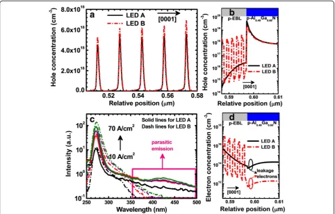
The two DUV LEDs differ from each other only in the p-EBL. Therefore, it is required to investigate the role of the superlattice p-EBL in improving the optical perform-ance for LED B. Figure3apresents the hole concentration profiles across the MQW region for LEDs A and B at the current density of 50 A/cm2. It is shown that the hole concentration level within the MQWs for LED B is higher than that for LED A. As has been reported, the p-EBL
reduces the electron leakage level while simultaneously hindering the hole injection [24]. A useful approach to reduce the hole blocking effect is to increase the hole concentration within the p-EBL region, which then helps to decrease the valence band barrier height [25]. Figure 3b then shows the hole concentration levels in the p-EBLs and the p-Al0.40Ga0.60N layers for LEDs A and
B at the current density of 50 A/cm2. The average hole concentration in the superlattice p-EBL for LED B is much higher than that for LED A by two orders of magnitude. The larger hole concentration in the superlattice p-EBL is well attributed to the excellent hole transport. Interest-ingly, if we further look into Fig.3b, we find that the hole concentration at the p-EBL/p-Al0.40Ga0.60N interface
become lower for LED A, which also reflects the smoother hole injection efficiency through the superlattice p-EBL for LED B.
As has been mentioned previously, the efficiency for LEDs is closely associated with the electron leakage level. Therefore, we show the measured EL spectra for LEDs A and B in a semi-log scale (see Fig. 3c) to indicate the detailed information regarding the parasitic luminescence.
Fig. 3Numerically calculated hole concentration profilesain the MQWs andbin the p-type hole injection layers for LEDs A and B, respectively;
[image:4.595.57.540.376.684.2]The peak emission wavelength for the parasitic lumines-cence is centered at ~ 425 nm, which may arise from the deep levels associated with Mg dopants [26]. The intensity of the parasitic luminescence for LED B is stronger than that for LED A, and it is speculated that more carriers recombine at the deep levels. In our experiment, the p-type hole injection layers for both DUV LED architec-tures are not engineered, and the hole concentration level in the hole injection layers shall be similar. Therefore, it is identified that electrons that escape from the MQW region possess a higher concentration in the hole injection layer for LED B than those for LED A. Our suggestions are further supported by Fig. 3dthat shows the electron concentration profiles in the p-type hole injection layers for LEDs A and B at the current density of 50 A/cm2. This also means that the electron leakage current has been
significantly reduced thanks to the superlattice p-EBL for LED B.
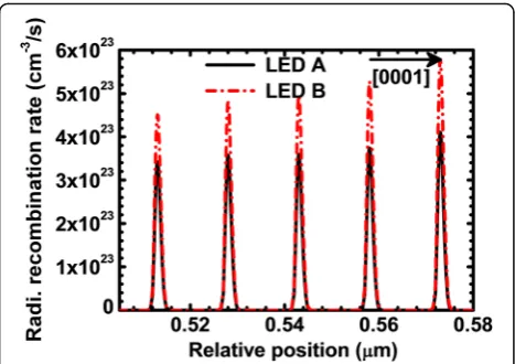
We then present the computed profiles of the radiative recombination rate for LEDs A and B in Fig.4which are collected at the current density level of 50 A/cm2. It is inferred that radiative recombination rate for LED B is stronger than that for LED A thanks to the proposed superlattice p-EBL, which even more favors the hole injection into the MQW region and suppresses the electron leakage level in the meantime.
Figure5aand 5bshow the energy band in the vicinity of the p-EBLs for both DUV LED devices. The energy bands are calculated at the current density of 50 A/cm2. As has been reported by Zhang et al. [27], the strong polarization induced positive charges at the last quantum barrier/p-EBL interface can significantly attract electrons, giving rise to the high local electron concentration. The high local electron concentration can reduce the effective conduction band barrier height (Øe) for the p-EBL which
is ~ 295 meV for LED A. If the bulk AlGaN based p-EBL is replaced by the specific superlattice p-EBL in this work (i.e., the superlattice p-EBL loop starts from the thin AlGaN layer with a smaller energy band gap than the last AlGaN quantum barrier), the conduction band for the last quantum barrier is titled upwards (see Fig. 5b), and this favors an electron depletion in the last quantum barrier which then increases the Øeto ~ 391 meV and enables a
smaller electron escape by means of thermionic emission [28]. Furthermore, the superlattice p-EBL facilitates the intra-band tunneling process for holes, as the result of which the hole concentration in the p-EBL also becomes higher (see Fig. 3b) The enhanced hole concentration in the p-EBL for LEDs tends to reduce the effective valence band barrier height (Øh) [25], i.e., the values ofØhare ~
324 meV and ~ 281 meV for LEDs A and B, respectively at
Fig. 4Numerically computed profiles of the radiative recombination rate for LEDs A and B. Data are collected at the current density level of 50 A/cm2
Fig. 5Numerically computed energy band profiles in the vicinity ofabulk AlGaN-based p-EBL for LED A,bsuperlattice p-EBL for LED B, andc
[image:5.595.57.291.87.252.2]the current density of 50 A/cm2. The even smallerØhfor
LED B in turn favors the thermionic emission for holes. It is worth noting that the superlattice p-EBL may also cause the intra-band tunneling for electrons. Fortunately, the improved hole concentration in the MQW can better consume electrons by radiative recombination, which also contributes to alleviate the electron leakage [12]. Because of the more favored hole injection and the even stronger recombination current that is produced by the radiative recombination process taking place in the MQW region, the forward voltage becomes smaller for LED B than that for LED A according to Fig.5c.
Conclusions
To summarize, this work has reported a specific super-lattice p-EBL for DUV LEDs, which can maintain both the promoted hole injection efficiency and the decreased electron leakage into the passive p-type hole injection layer. Therefore, both numerically and experimentally, the improved EQE and the remarkably suppressed effi-ciency droop are obtained. We strongly believe that the proposed DUV LED structure is very promising for real-izing high-efficiency DUV LEDs and the device physics revealed by this work introduces more understanding to the III-nitride-based optoelectronic community.
Abbreviations
APSYS:Advanced Physical Models of Semiconductor Devices; DUV: Deep ultraviolet light-emitting diodes; EL: Electroluminescence; EQE: External quantum efficiency; HVPE: Hydride Vapor Phase Epitaxy; ICP: Inductively Coupled Plasma; IQE: Internal quantum efficiency; LEE: Light extraction efficiency; MOCVD: Metal-organic chemical vapor deposition; MQWs: Multiple quantum wells; p-EBL: p-type electron blocking layer; TDD: threading dislocation density
Authors’Contribution
ZHZ and HCK designed the experiment and the physical modeling and co-wrote the manuscript. SWHC prepared the samples and conducted the measurement. CC and KT made the simulations. YZ and WB co-wrote the manuscript. All authors read and approved the final manuscript.
Funding
This work is support by the National Natural Science Foundation of China (Project Nos. 51502074, 61604051), Natural Science Foundation of Hebei Province (Project No. F2017202052), Natural Science Foundation of Tianjin City (Project No. 16JCYBJC16200), Program for Top 100 Innovative Talents in Colleges and Universities of Hebei Province (Project No. SLRC2017032), and Program for 100-Talent-Plan of Hebei Province (Project No. E2016100010).
Availability of Data and Materials
The data and the analysis in the current work are available from the corresponding authors on reasonable request.
Competing Interests
The authors declare that they have no competing interests.
Publisher’s Note
Springer Nature remains neutral with regard to jurisdictional claims in published maps and institutional affiliations.
Received: 8 March 2018 Accepted: 16 April 2018
References
1. Li L, Zhang Y, Xu S, Bi W, Zhang Z-H, Kuo H-C (2017) On the hole injection for III-nitride based deep ultraviolet light-emitting diodes. Material 10(10):1221 2. Khan A, Balakrishnan K, Katona T (2008) Ultraviolet light-emitting diodes
based on group three nitrides. Nat Photonics 2(2):77–84
3. Kneissl M, Kolbe T, Chua C, Kueller V, Lobo N, Stellmach J, Knauer A, Rodriguez H, Einfeldt S, Yang Z, Johnson NM, Weyers M (2011) Advances in group III-nitride-based deep UV light-emitting diode technology. Semicond Sci Tech 26(1):014036
4. Shatalov M, Sun W, Lunev A, Hu X, Dobrinsky A, Bilenko Y, Yang J, Shur M, Gaska R, Moe C, Garrett G, Wraback M (2012) AlGaN deep-ultraviolet light-emitting diodes with external quantum efficiency above 10%. Appl Phys Express 5(8):082101
5. Ryu H-Y, Choi I-G, Choi H-S, Shim J-I (2013) Investigation of light extraction efficiency in AlGaN deep-ultraviolet light-emitting diodes. Appl Phys Express 6(6):062101
6. Kim M-H, Schubert MF, Dai Q, Kim JK, Schubert EF, Piprek J, Park Y (2007) Origin of efficiency droop in GaN-based light-emitting diodes. Appl Phys Lett 91(18):183507
7. Katsuragawa M, Sota S, Komori M, Anbe C, Takeuchi T, Sakai H, Amano H, Akasaki I (1998) Thermal ionization energy of Si and Mg in AlGaN. J Crystal Growth 189:528–531
8. Mehnke F, Kuhn C, Guttmann M, Reich C, Kolbe T, Kueller V, Knauer A, Lapeyrade M, Einfeldt S, Rass J, Wernicke T, Weyers M, Kneissl M (2014) Efficient charge carrier injection into sub-250 nm AlGaN multiple quantum well light emitting diodes. Appl Phys Lett 105(5):051113
9. Guo W, Xu F, Sun Y, Lu L, Qin Z, Yu T, Wang X, Shen B (2016) Performance improvement of AlGaN-based deep-ultraviolet light-emitting diodes by inserting single spike barriers. Superlattices Microst 100:941–946 10. Tan S, Egawa T, Luo XD, Sun L, Zhu YH, Zhang C (2016) Influence of barrier
height and p-cladding layer on electroluminescent performance of AlGaN deep ultraviolet light-emitting diodes. J Phys D Appl Phys 49(12):125102 11. Chang JY, Chang HT, Shih YH, Chen FM, Huang MF, Kuo YK (2017) Efficient
carrier confinement in deep-ultraviolet light-emitting diodes with composition-graded configuration. IEEE T Electron Dev 64:4980 12. Piprek J, Li ZMS (2013) Origin of InGaN light-emitting diode efficiency
improvements using chirped AlGaN multi-quantum barriers. Appl Phys Lett 102(2):023501
13. Zhang Z-H, Li LP, Zhang YH, Xu FJ, Shi Q, Shen B, Bi WG (2017) On the electric-field reservoir for III-nitride based deep ultraviolet light-emitting diodes. Opt Express 25(14):16550–16558
14. Kuo YK, Chang JY, Chen FM, Shih YH, Chang HT (2016) Numerical investigation on the carrier transport characteristics of AlGaN deep-UV light-emitting diodes. IEEE J Quantum Elect 52(4):3300105
15. Li S, Ware ME, Wu J, Kunets VP, Hawkridge M, Minor P, Wang Z, Wu Z, Jiang Y, Salamo GJ (2012) Polarization doping: reservoir effects of the substrate in AlGaN graded layers. J Appl Phys 112:053711
16. Li S, Zhang T, Wu J, Yang Y, Wang Z, Wu Z, Chen Z, Jiang Y (2013) Polarization induced hole doping in graded AlxGa1-xN (x=0.7 ~ 1) layer grown by molecular beam epitaxy. Appl Phys Lett 102:062108 17. Li S, Ware M, Wu J, Minor P, Wang Z, Wu Z, Jiang Y, Salamo GJ (2012)
Polarization induced pn-junction without dopant in graded AlGaN coherently strained on GaN. App Phys Lett 101:122103
18. Zhang Z-H, Chen S-WH, Zhang YH, Li LP, Wang S-W, Xu S, Tian KK, Chu CS, Fang MQ, Kuo H-C, Bi WG (2017) Hole transport manipulation to improve the injection for deep ultraviolet light-emitting diodes. ACS Photon 4(7): 1846–1850
19. Park JH, Kim DY, Hwang S, Meyaard D, Schubert EF, Han YD, Choi JW, Kim JK (2013) Enhanced overall efficiency of GaInN-based light-emitting diodes with reduced efficiency droop by Al-composition-graded AlGaN/GaN superlattice electron blocking layer. App Phys Lett 103:061104 20. Lee S-J, Han S-H, Cho C-Y, Noh DY, Shim H-W, Kim YC, Park S-J (2011)
22. Huang J, Guo Z, Guo M, Liu Y, Yao S, Sun J, Sun H (2017) Study of deep ultraviolet light-emitting diodes with a p-AlInN/AlGaN superlattice electron-blocking layer. J Electron Mater 46(7):4527–4531
23. Wang S, Yin YA, Gu H, Wang N, Liu L (2016) Graded AlGaN/AlGaN superlattice insert layer improved performance of AlGaN-based deep ultraviolet light-emitting diodes. J Display Technol 12(10):1112–1116 24. Han S-H, Lee D-Y, Lee S-J, Cho C-Y, Kwon M-K, Lee SP, Noh DY, Kim D-J,
Kim YC, Park S-J (2009) Effect of electron blocking layer on efficiency droop in InGaN/GaN multiple quantum well light-emitting diodes. Appl Phys Lett 94(23):231123
25. Zhang Z-H, Chu CS, Chiu CH, Lu TC, Li LP, Zhang YH, Tian KK, Fang MQ, Sun Q, Kuo H-C, Bi WG (2017) UVA light-emitting diode grown on Si substrate with enhanced electron and hole injections. Opt Lett 42(21):4533–4536 26. Norimichi N, Hirayama H, Yatabe T, Kamata N (2009) 222 nm single-peaked
deep-UV LED with thin AlGaN quantum well layers. Phys Status Solidi C 6: S459–S461
27. Zhang Z-H, Liu W, Ju ZG, Tan ST, Ji Y, Zhang XL, Wang LC, Kyaw Z, Sun XW, Demir HV (2014) Polarization self-screening in [0001] oriented InGaN/GaN light-emitting diodes for improving the electron injection efficiency. Appl Phys Lett 104(25):251108