FIR1l
HEWLETT
a:~
PACKARD
HP 27112A
GENERAL PURPOSE 1/0 INTERFACE (GPIO)
PRINTING HISTORY
First Edition ... December 1982
NOTICE
Installation Manual
Card Assembly: 27112-60001 Date Code: B-2232
Manual Part Number 27112-90001
The information contained in this document is subject to change without notice.
HEWLETT-PACKARD MAKES UO WARRANTY OF ANY KIND WITH REGARD TO THIS MATERIAL, INCLUDING, BUT NOT LIMITED TO, THE IMPLIED WARRANTIES OF MERCHANT ABILITY AND FITNESS FOR A PARTICULAR PURPOSE. Hewlett-Packard shall not be liable for errors contained herein or for incidental or consequential damages in con-nection with the furnishing, performance, or use of this manual.
This document contains proprietary information which is protected by copyright. All rights are reserved. No part of this document may be photocopied or reproduced without the pri9f written consent of Hewlett-Packard Company.
ThIS manual provides information for you to install and verify correct operation of the HP 27112A General Purpose I/O Interface (GPIO) card. You will also need the appropriate computer system installation manual. These two manuals should provide all the required information. If your installation is such that you need additional information concerning the GPIO card, order the HP 27132A Technical Reference Package from the nearest Hewlett-Packard Sales and Service Office.
Installation and Checkout
To install and check the operation of the GPIO card, follow the steps below in the order given:
1. Determine if your computer system can supply the power needed for the GPIO card. Refer to table 1 for power requirements.
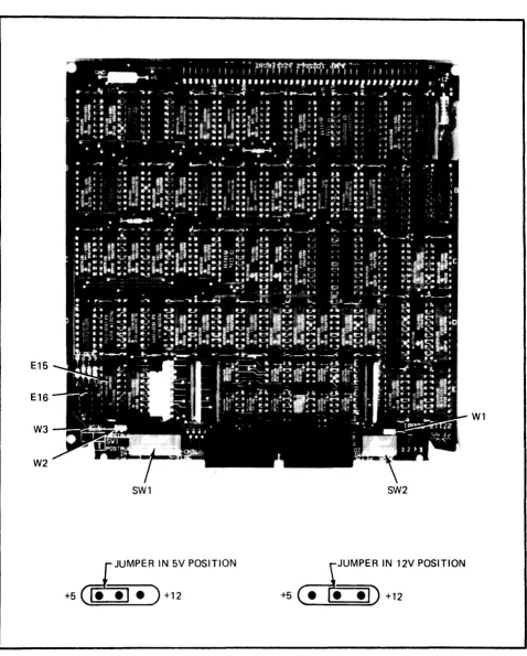
2. Install jumpers in WI, W 2, and W 3, depending on whether 5 -volt or 1 2 -volt logic levels are to be used. The locations of WI, W2, and W3, and the positions of the jumpers for +5-volt or +12-volt operation are shown in figure 1.
3. Set the card's switches for proper operation in your system. Refer to tables 2, 3, and 4 for switch information. Actual switch settings will vary according to the computer system and the device which is connected to the GPIO card. However, switch settings for the HP 9885 disc drive (a typi-cal device used with the GPIO) are shown below:
DEVICE SW1 SW2
1 2 3 4 5 6 7 8 1 2 3 4 5
HP 9885 Disk Drive
C C C C C C 0 C 0 0 0 C 0o
==open
C • clo!led
4. There are two one-shots (E 15, see figure 1) on the GPIO card which generate the write delay and the internal handshake delay. The write delay one-shot provides approximately 100 nsec for the output data to settle. When extra long cables are used, or when the peripheral device requires ad-ditional settling time for the data, the delay can be increased by adding a capacitor between pins 1 and 4 of the socket at E 16 (see figure 1 for location of E 16).
The formula for selecting the capacitor value is:
C
=
(T -
100)/1.5where
E15
E16
W3
W2
SW1
f
JUMPER IN 5V POSITION+5~+12
SW2
~JUMPER IN 12V POSITION
[image:3.613.72.550.55.650.2]+5~+12
Figure 1. Switch and Jumper Locations
The internal delay one-shot provides a delay of approximately 3 usec between the assertion of PCNTL and the assertion of FLAG. The delay can be increased by adding a capacitor between pins 5 and 8 of the socket at E 16 (see figure 1 for location of E 16).
The formula for the value of the capacitor is:
C • (T -
3000)/3
where,
C
=
additional capacitance (in pf)
T
=
total time delay required (in n5ec)
5. Install the card in the appropriate slot in the computer. Refer to the computer system in-stallation manual to determine the correct slot.
6. Connect the cable, supplied with the card, from J2 on the card to the peripheral device. If you ha ve the test hood, which exercises more of the card's circuitry, and can be ordered (Hewlett-Packard part number 1251-8003), connect it to J2 instead of connecting the cable.
7. Turn on computer system power.
8. Run the card verification program. Refer to the appropriate host computer system manual for information on running this program.
9. If a test hood was used, turn off computer power and remove the test hood. Connect the cable and, if necessary, reset the switches for your application.
Reshipment
If the GPIO is to be shipped to Hewlett-Packard for any reason, attach a tag identifying the owner and indicating the reason for shipment. Include the part number of the GPIO.
Table 1. Power Requirements
+5V OUTPUT
+12V OUTPUT
VOLTAGE
CURRENT
POWER
CURRENT
POWER
+5V
2.2A
10.g"j
2.1 A
1 0.6W
+12V
0
0
o
.15A
1.8W
TOTAL
DISSIPATION
10.g"j
12.2W
Table 2. Configuration Switch SW 1 Definitions
SWITCH ASSEMBLY SW1
-
LOGIC SENSE SELECTION
SWITCH
CONTROLS
OPEN
CLOSED
S1
DIN[15:0]
POSITIVE TRUE
NEGATIVE TRUE
S2
CTL[1 :0] and STS[1 :0] POSITIVE TRUE
NEGATIVE TRUE
53
PSET
POSITIVE TRUE
NEGATIVE TRUE
S4
PDIR
POSITIVE TRUE
NEGATIVE TRUE
S5
DOUT[15:0]
POSITIVE TRUE
NEGATIVE TRUE
S6
PEND
POSITIVE TRUE
NEGATIVE TRUE
S7
PFLAG
POSITIVE TRUE
NEGATIVE TRUE
BUSY
=
HIGH
BUSY
=
LOW
READY
=
LOW
READY
=
HIGH
[image:5.613.72.547.118.279.2] [image:5.613.75.547.370.696.2]Table 3. Configuration Switch SW2 Definitions
SWITCH ASSEMBLY SW2 -
HANDSHAKE CONFIGURATION
SWITCH
CONTROLS
OPEN
CLOSED
S1
BIDIRECTIONAL BUS ENABLE
DISABLED
ENABLED
S2
INTERNAL HANDSHAKE ENABLE
DISABLED
ENABLED
S3
PULSE HANDSHAKE ENABLE
DISABLED
ENABLED
S4
INPUT CLOCK SEL 0
SEE TABLE 4
55
INPUT CLOCK SEL 1
SEE TABLE 4
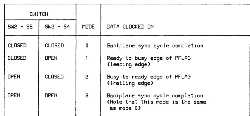
Table 4. Switch Settings for Data Input Register Clock Selection
SWITCH
SW2 -
55SW2 - S4
MODE
DATA CLOCKED ON
CLOSED
CLOSED
0
Backplane sync cycle completion
CLOSED
OPEN
1Ready to busy edge of PFLAG
(leading edge)
OPEN
CLOSED
2
Busy to ready edge of PFLAG
(trailing edge)
OPEN
OPEN
3Backplane sync cycle completion
(Note that this mode is the same
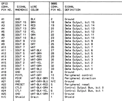
[image:6.615.69.544.116.324.2] [image:6.615.62.545.389.613.2]Table 5. Device Connector J2
GPIO
9885
CONN.
SIGNAL
WIRE
CONN.
SIGNAL
PIN NO.
MNEMONIC COLOR
PIN NO.
DEFINITION
A1
GND
BLK
2
Ground
A2
DOUT 15
BRN
18
Data Output) bit 15
A3
DOUT 14
RED
19
Data Output) bit 14
A4
DOUT 13
ORN
20
Data Output) bi t 13
AS
DOUT 12
YEL
21
Data Output) bi t 12
AS
DOUT 11
GRN
22
Data Output) bi t 11
A7
DOUT 10
BLU
23
Data Output) bit 10
A8
DOUT 9
VIO
24
Data Output) bit 9
A9
DOUT 8
GRY
25
Data Output) bi t 8
A10
DOUT 7
WHT
26
Data Output) bi t 7
A11
~DOUT 6
WHT-BLK
27
Data Output) bit 6
A12
DOUT 5
WHT-BRN
28
Data Output) bit 5
A13
DOUT 4
WHT-RED
29
Data Output) bi t 4
A14
DOUT 3
WHT-ORN
30
Data Output, bit 3
A15
DOUT 2
WHT-YEL
31
Data Output, bi t 2
A1S
DOUT 1
WHT-GRN
32
Data Output, bi t 1
A17
DOUT 0
WHT-BLU
33
Data Output, bit 0
A18
GND
WHT-VIO
8
Ground
A19
PCNTL
WHT-GRY
10
Peripheral control
A20
PDIR
WHT-BLK-BRN 15
Peripheral direction
A21
GND
WHT-GRN-BLU
NICGround
A22
PRESET
WHT-BLK-RED 5
Peripheral reset
A23
CTLO
WHT-BLK-ORN 4
Control Output Bus, bit 0
A24
CTL1
WHT-BLK-YEL 6
Control Output Bus, bit 1
A25
GND
WHT-BLK-GRN 11
Ground
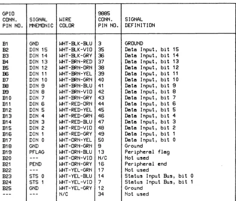
[image:7.615.72.545.105.497.2]Table 5. Device Connector J2 (Continued)
GPIO
9885
CONN.
SIGNAL
WIRE
CONN.
SIGNAL
PIN NO.
MNEMONIC COLOR
PIN NO.
DEFINITION
81
GND
WHT-BLK-BLU 3
GROUND
82
DIN 15
WHT-BLK-VIO 35
Data Input, bi t 15
83
DIN 14
WHT-BLK-GRY
36Date Input, bit 14
B4
DIN 13
WHT-BRN-RED 37
Data Input, bi t 13
85
DIN 12
WHT-BRN-ORN
38Data Input, bit 12
B6DIN 11
WHT-BRN-YEL
39Data Input, bi t 11
B7
DIN 10
WHT-BRN-GRN 40
Data Input, bi t 10
B8
DIN 9
WHT-BRN-BLU 41
Data Input, bit 9
B9DIN 8
WHT-8RN-VIO 42
Date Input, bit 8
810
DIN 7
WHT-BRN-GRY 43
Data Input, bit 7
811
DIN 6
WHT-RED-ORN 44
Date Input, bit 6
812
DIN 5
WHT-RED-YEL 45
Date Input, bit 5
B13
DIN 4
WHT-RED-GRN 46
Data Input, bit 4
814
DIN 3
WHT-RED-8LU 47
Date Input, bit 3
815
DIN 2
WHT-RED-VIO 48
Data Input, bit 2
B16
DIN 1
WHT-RED-GRY 49
Data Input, bit 1
B17
DIN 0
WHT-ORN-YEL 50
Data Input, bit 0
818
GND
WHT-ORN-GRN 9
Ground
819
PFLAG
WHT-ORN-8LU 13
Peripheral flag
820
---
WHT-ORN-VIO
N/CNot u5ed
821
PEND
WHT-ORN-GRY 16
Peripheral end
822
---
WHT-YEL-GRN 17
Not u5ed
823
STS 0
WHT-YEL-8LU 14
Statu5 Input BU5, bi t 0
824
STS 1
WHT-YEL-VIO 7
Statu5 Input 8U5, bi t 1
825
GND
WHT-YEL-GRY 12
Ground
[image:8.615.70.544.107.510.2]Flin-
HEWLETT
.:~
PACKARD
MANUAL PART NO. 27112-90001 Printed in U.S.A
December, 1982