5
IV
April 2017
Technology (IJRASET)
A Comparative Performance Analysis of Various
CMOS Design Techniques for XOR and XNOR
Circuits
Aditi Joshi 1, Chanchal Jain 2, Pooja Choudhary3, Chirag Arora4, Krishan Rapswal 5
1,2,4,5
Deptt. of Electronics and Comm. Engg., SKIT, M&G, Jaipur, (RAJ.) INDIA
3
Asst. Prof., Deptt. of Electronics and Comm. Engg., SKIT, M&G, Jaipur, (RAJ.) INDIA
Abstract: XOR and XNOR gates play an important role in digital systems. XOR & XNOR logic gates are basic building blocks of many arithmetic circuits. The XOR and XNOR circuit is implemented in pass transistor logic, static CMOS logic, transmission gate logic. The design of the XOR & XNOR circuits based on TSMC 32nm process models at the supply voltage 0.9V is simulated using HSPICE. Due to low power consumption and high speed these design circuits are suitable for arithmetic operations and VLSI applications. Hence comparison of delay & power is obtained in this paper for various design techniques of logic gates.
Keywords: HSPICE, Low power, pass transistor logic, transmission gate, Exclusive-OR, Exclusive-NOR
I. INTRODUCTION
To design integrated circuits with high operating frequency the major issues are power, delay and smaller silicon area with higher speed. The XOR and XNOR circuits influence the performance of the complex logic circuits. The key parameter for today’s electronic industry is low power. In order to make a device more reliable and efficient, power consumption should be reduced. As the demand of portable consumer electronics increases, and the size of the chip decreases, challenges towards the power dissipated are induced [1-3].
In CMOS circuit, the power consumption for any given function must be reduced for two different reasons: the first reason is to reduce heat dissipation in order to allow a large density of functions to be incorporated on an IC chip. Any amount of power consumption is fruitful as long as it doesn’t degrade overall circuit performance [4]. The second reason is to save energy in battery operated instruments. By choosing proper design style the power saving capability in circuits can increase at the design level. Without low-power design techniques such applications generally suffer from very short battery life, while packaging and cooling them would be very difficult. This is leading to an unavoidable increase in the cost of the product.
A. Static CMOS Logic
It is the most commonly used logic design technique. This circuit is made up of two networks namely pull up network (PUN) and pull down network (PDN). PUN and PDN comprises of PMOS transistors and NMOS transistors respectively. Input to these networks is dual of each other [5]. Output is based on the inputs applied to PUN and PDN making the output 1 or 0 respectively. This design technique is mostly used and produces results that are widely accepted but it requires more number of CMOS.
B. Pass Transistor Logic
The static Gate with low-impedance path exists. In this logic design, the reduction in output voltage swing is useful for power consumption as well as for slow switching. Less number of transistors are difficulty to design [7].
C. Transmission Gate Logic
Transmission gate CMOS (TG) uses complex logic functions by using complementary transistors. PMOS and NMOS are in parallel and are controlled by complementary signals. Both transistors are ON or OFF simultaneously [8].
The NMOS switch passes a good zero but a poor 1. The PMOS switch passes a good one but a poor 0.
Technology (IJRASET)
II. CIRCUITDESIGNA. Static CMOS XOR and XNOR Circuit
Complementary CMOS uses dual networks to implement a given function [9-11]. A first part consists solely of complementary pull-up (PMOS) network while a second part consists of pull-down (NMOS) networks. This technique is popular and produces results that are widely accepted but it requires more numbers of CMOS transistors. Static CMOS XOR and XNOR gate is shown in Fig.2.1(a) and Fig.2.1(b). The circuit operates with full output voltage swing.
Z = A ⊕B = (A + B). (A′ + B′)
Z′ = (A ⊕B) ′ = {(A + B). (A′ + B′)} ′
Z′ = AB + A′B′
Z = (AB + A′B′) ′ = A ⊕B
Fig.2.1 (a) Static CMOS XOR circuit.
Fig.2.1 (b) Static CMOS XNOR Circuit
B. PTL based XOR and XNOR Circuits
Technology (IJRASET)
Fig.2.2 (b) Pass Transistor XNOR Circuit
C. Transmission Gate based XOR and XNOR Circuits
It solves the problem of low logic level swing by using PMOS as well as NMOS. The circuits for XOR-XNOR function is shown in Fig. 2.3(a) alleviate the problems of threshold voltage loss and non-zero standby power dissipation. By cascading a standard inverter after the XOR circuit, a high performance XNOR, as shown in Fig. 2.3(b) will have a restored output. The same property is present in the XOR structure. These circuits provide a full voltage swing (i.e., 0V for logic 0 and 1.8V for logic 1) [12-13].
Fig.2.3 (a) Transmission Gate XOR Circuit
[image:4.612.212.390.94.222.2] [image:4.612.229.367.335.465.2] [image:4.612.237.399.506.688.2]Technology (IJRASET)
III.SIMULATIONRESULTSThe transient and DC analysis of the circuits were performed on HSPICE at a supply voltage ranging 0.9V using TSMC 32nm CMOS process. The simulation results of various XOR and XNOR designs are shown in Fig.3.1-3.6.
Fig.3.1 Static CMOS XOR Waveform
Fig.3.2 Static CMOS XNOR Waveform
Technology (IJRASET)
Fig.3.4 Pass Transistor XNOR Waveform
Fig.3.5 Transmission gate XOR Waveform
Fig.3.6 Transmission gate XNOR Waveform
IV.COMPARISON
Technology (IJRASET)
TABLE I
Comparative performance of transient analysis of XOR circuits with different design techniques at Vdd = 0.9V
Parameter XOR Static CMOS Logic Pass Transistor Logic Transmission Gate Logic Number of Transistor
12 4 2
tplh
9.0851E-09
3.0510E-10
5.2327E-11
tphl
1.3190E-11
1.6685E-10
2.0933E-11
Delay
4.5491E-09 2.3598E-10 3.6630E-11 Average Power 1.9658E-06 7.9505E-07 9.8448E-05 Maximum Power 7.8521E-05 2.6015E-05 1.6720E-04
PDP
8.9426E-15
1.8761E-16
1.3417E-15
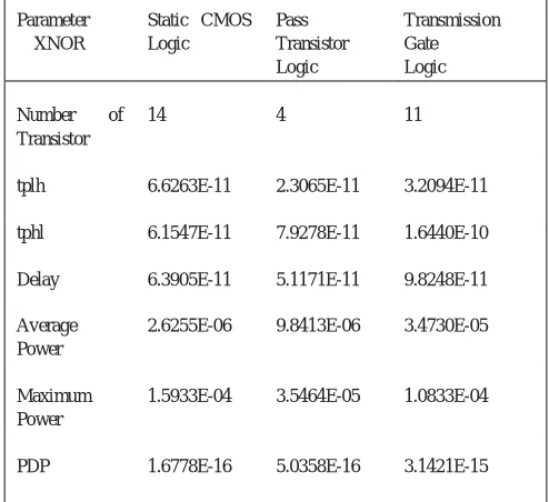
TABLE II
Comparative performance of transient analysis of XNOR circuits with different design techniques at Vdd = 0.9V
Parameter XNOR
Static CMOS Logic Pass Transistor Logic Transmission Gate Logic
Number of
Transistor
14 4 11
tplh 6.6263E-11 2.3065E-11 3.2094E-11
tphl 6.1547E-11 7.9278E-11 1.6440E-10
Delay 6.3905E-11 5.1171E-11 9.8248E-11
Average Power
2.6255E-06 9.8413E-06 3.4730E-05
Maximum Power
1.5933E-04 3.5464E-05 1.0833E-04
[image:7.612.182.429.480.706.2]Technology (IJRASET)
V. CONCLUSION
In this paper, we have studied various design techniques for XOR-XNOR circuits. The mentioned design techniques are compared based on area, delay, power consumption, and PDP. The performances of these techniques have been evaluated by HSPICE using a TSMC 32nm CMOS technology. These design techniques are suitable for arithmetic circuits and other VLSI applications with very low power consumption and a very high speed performance. Based on the simulation results, it has been culminated that in the PTL based XOR and XNOR design the output high (or low) voltage is deviated from the VDD (or ground) by a multiple of threshold voltage. The XOR-XNOR circuits using transmission gate improve the threshold voltage loss problem while XOR and XNOR circuits with feedback transistors have good output signal levels, consume less power and have high speed compared to the previous designs at low supply voltage.
VI.ACKNOWLEDGMENT
This work has been done in Project lab, Electronics &Communication Department. The authors would like to thank Director (Academics) and the Management of SKIT, Jaipur for permission to carry out this work.
REFERENCES
[1] N. Weste, K. Eshranghian, Principles of CMOS VLSI Design: A System Perspective, Reading MA: Addison-Wesley, (1993). [2] Sung-Mo Kang, Y. Leblibici, CMOS Digital Integrated Circuits: Analysis and Design, Addition-Tata McGraw Hill, (2003). [3] J.Rabaey, Digital Integrated Circuits (A Design Prospective), Prentice-Hall, Englewood Cliffs, NJ, (1996).
[4] Sung-Chuan Fang, Jyh-Ming Wang, Wu-Shiung Feng, A New Direct design for three-input XOR function on the transistor level, IEEE Trans. Circuits Syst. I: Fundamental theory and Applications, 43(4): (1996).
[5] K.H. Cheng and C.S. Huang, The novel efficient design of XOR/XNOR function for adder applications, in Proc. IEEE Int. Conf. Elect., Circuits Syst., 1: 29-32(1999).
[6] M. Vesterbacka, A New six-transistor CMOS XOR Circuits with complementary output, to appear in Proc. 42nd Midwest Symp. On Circuits and Systems, Las Cruces, NM, Aug., 8-11(1999).
[7] R. Zimmermann, W. Fichtner, Low-power logic styles: CMOS versus pass-transistor logic, IEEE J. Solid-State Circuits, 32(7): 1079-1090(1997).
[8] D. Radhakrishanan, S.R. Whitaker, G.K. Maki, Formal design procedures for pass-transistor switching circuits, IEEE J. Solid-State Circuits, 20(3): 531-536(1985).
[9] C. Pedron, A. Stauffer, Analysis and synthesis of combinational pass transistor switching circuits, IEEE Trans. Computer-Aided Design Integer. Circuit Syst., 7(7):775-786(1988).
[10] H. Lee and G. E. Sobelman, New low-voltage circuits for XOR and XNOR, in Proc. IEEE Southeastcon, Apr. 12-14, pp. 225-229(1997).
[11] A.M. Shams, T.K. Darwish, M.A. Bayoumi, Performance analysis of low-power 1-bit CMOS full adder cells, IEEE Trans. Very Large Scale Integr. (VLSI) Syst., 10(1): 20-29(2002).
[12] H. Lee and G.E. Sobelman, New XOR/XNOR and Full adder circuits for low voltage, low power application, Microelectronics Journal 29: 509-517(1998). [13] Sumeer Goel, Mohammed A Elgamel and MA Bayoumi, Design Methodologies for High-Performance Noise-Tolerant XOR-XNOR Circuits, IEEE Trans.