Technology (IJRASET)
Automatic Power Controllers Used for Power
Consumption in AC-to-DC LED Drivers
V. Mahesh Kumar1, T.Poornipriya2
1
Assistant Professor, 2PG Student
1,2
Department of Electrical and Electronics,Jay Shri Ram Group Of Institutions, Tirupur, India
Abstract— A novel control scheme of quasi-resonant (QR) mode and valley-switching for high-power-factor (PF) ac-to-dc light-emitting diode (LED) drivers. The proposed driver control scheme is based on a buck PF corrector converter, which is operated in QR valley-switching. The proposed control scheme can directly sense the QR valley signal from the current sensor, and it is definitely different from the conventional method which senses the QR valley signal from auxiliary winding. The cost and size of the driver circuit can be remarkably reduced when the proposed control scheme is adopted. Furthermore, the proposed circuit can provide not only high PF and low total harmonic distortion but also high conversion efficiency. Up to 0.99 PF and 91.5% efficiency are obtained from an 8-W (40-W replaced) LED bulb driver prototype.
Keywords— Fuzzy logic (FL), Bridgeless (BL) buck–boost converter, discontinuous inductor current mode (DICM), power factor correction (PFC).
I. INTRODUCTION
Nowadays ,since the improvements in process and technology ,the luminous-efficiency of light-emitting-diodes (LED’s) is significantly enhanced .As compared with other light sources ,for instance ,high intensity discharge lamps (HID), fluorescent lamps(FL), and cold=cathode fluorescent lamps(CCFL),LED has considerable advantages on mercury-free device ,low dc voltage driving , and ultra long lifetime(above 50,000 hours).Due to the international petroleum crisis and greenhouse effect , the whole world looks forward to the more efficient luminaries and thus the conventional light sources are progressively replaced by LEDs. In general, the driver circuit design dominates the energy efficiency as significantly as the light sources. In other words, the lighting product efficiency can be considerably improved via an appropriate driver circuit. Besides acquiring electrical energy from the wall plugs (ac line voltage source) is the familial way .However, LED’s are more suitable to be driven by dc voltage in accordance with their characteristics, and thus an ac-to-dc conversion stage is necessary. Furthermore, the switching converter is one of the most common and efficient LED driving solutions. In general, conventional ac-to-dc switching converters are constructed from a diode-bridge rectifier followed by a bulk capacitor and a dc-to-dc switching converter. This topology has inherent drawbacks, such as the poor performances in power factor and total harmonic distortion (THD) .Therefore, an additional power factor correction (PFC) stage is associated with the current harmonics regulations and improves the power factor at the same time. Inspite of its good performance, the two-stage solutions are usually more inefficient and have lower cost/ performance (C/P) ratio.
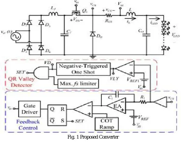
For the sake of improving the above disadvantages and reducing the driver cost, there are several topologies for LED driver circuits that have been developed consequently .Although these LED driver circuits have many advantages, their efficiencies are usually not good enough (about 80%) . In order to enhance the power efficiency, the quasi-resonant (QR) valley-switching is one of the most familiar methods .The QR valley-switching is achieved by the L-C resonant tank, which is composed of the main inductance and the parasitic capacitance of the power MOSFET .In this way, the power MOSFET will be switched on once the drain-to-source voltage resonates to the lowest value and to minimize the switching loss, this technique is called valley-switching. However ,the conventional control scheme of QR valley-switching senses the valley signal from an auxiliary winding, as shown in fig 1,which hinders the magnetic core selection, and further raises the driver cost and size.
II. PROPOSED BUCK CONVERTER FEEDING LED DRIVES
done by the voltage feedback control of the converter along with the filter operation. The switching stress will also be evaluated along with the other parameters so that the design of heat sinks can be done easily. The circuit is operating in three modes in each of the half cycles. Lf and Cf are the filter inductance and capacitance at the input stage. SW1 and Sw2 are the switches, L1 and L2 are the inductors, D1 and D2 are the diodes in the dual buck boost converter. The inverter switches are numbered through S1 to S6 and the BLDC motor drive employed with Hall Effect position (Ha-Hc) sensors are also shown in the circuit.
Fig. 1 Proposed Converter
III. OPERATION OF BUCK CONVERTER
The converter is a dual buck boost converter operating in both positive and negative half cycles of input supply voltage. It is performed in three different modes in each of the half cycles which is given below.
A. Operation during high voltage and low voltage
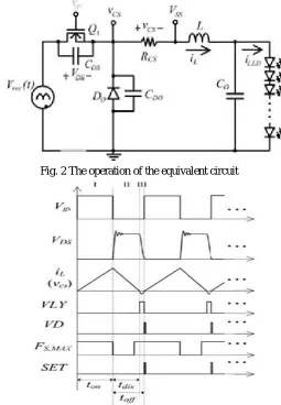
Mode 1: In mode I q1 is switched on imposing vrec on the inductor L. since L is operated in BCM and DCM to achieve PFC,
inductor current i1, increase linearly from zero and rising slopes of iL is proportional to the difference of vrec and Vled. Il keeps
increasing until Q1 is switched off, at which instant iL reaches its peak value within the switching cycle.
Mode 2: During this mode of operation, iL declines the peak continuously. The down slope of iL depends on the output voltage,Vled.
The upload and peak value of iL is proportional to the difference of Vrec and Vled. Thus the duration that iL declines to zero varies
with Vrec. It means that the discharging time of iL is varied with the BCM and DCM PFC operation, and thus the switching
frequency may be varied with Vrec. This mode ends when iL, drop to zero and the operation proceed to next mode.
Mode 3: At beginning of this mode, the inductor current iL has declined to zero. The main inductance L and the parasitic
capacitance from a resonant tank. The equivalent circuit is shown in fig 2. The main inductance L resonant with Cf, the
Technology (IJRASET)
Fig. 2 The operation of the equivalent circuit
Fig. 3 Theoretical waveform of the equivalent circuit
B. Circuit analysis
Besides parasitic capacitance of power MOSFET Q1 and freewheeling diode Do, all other component are ideal. The capacitance Cf is small, and the EMI filter is eliminated Vrec ispurely rectified sinusoidal voltage source .The output capacitance Co is large, so that
the Led can be regarded as dc voltage. According to the operation principles, this section QR-valley with high power factor ac-to-dc LED driver circuit.
The LED driver circuit supplied by the line voltage source,
vac(t)= Vmsin(2πf Lt)
where Vm and fL are the amplitude and frequency of the line voltage source
[image:4.612.201.410.574.659.2]Fig. 5The input equivalent circuit of buck PFC
C. Experimental Result
[image:5.612.80.546.37.225.2]The input EMI filter (Lf and Cf) applied to filter out the switching frequency noise. Although larger Lf and Cf better noise Filtering Increase the cost and size.
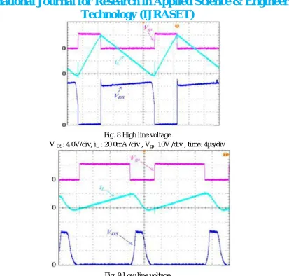
Fig 6 shows the switching waveform of Vds, iL, and Vgs. The observed waveform prove that the QR-switching valley operations properly without any deviation from the assumption and analysis with the fig and thus the improvement in the circuit efficiency and EMI performance can be achieved. It can be observed that the circuit is approximately operated in BCM at first valley switching (110V) and the line voltage operated under DCM are second valley switching (220V).
The variation of power factor and circuit efficiency in the Vac range from 85Vrms to 265Vrms. To limit the harmonic content class D device is used when the input power is smaller than 25W.
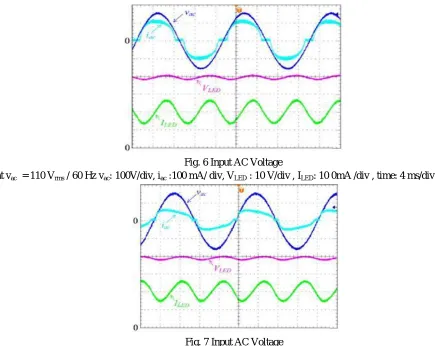
Fig. 6 Input AC Voltage
at vac = 110 Vrms / 60 Hz vac: 100V/div, iac :100 mA/ div, VLED : 10 V/div , ILED: 10 0mA /div , time: 4 ms/div
Fig. 7 Input AC Voltage
[image:5.612.91.531.353.699.2]Technology (IJRASET)
Fig. 8 High line voltage
[image:6.612.110.523.47.441.2]V DS: 4 0V/div, iL : 20 0mA /div , Vgs: 10V /div , time: 4µs/div
Fig. 9 Low line voltage
V DS: 20V/ div, i L: 50 mA /div, Vgs: 10V /div, time : 2µs/div Fig. 9 W ave forms of VDS, iL, Vgs @ vac= 110 Vrms/ 60Hz
IV. SIMULATION RESULTS
The performance of the proposed system of QR-valley switching scheme can dectect the valley from current sense resistance. The auxiliary winding can be eliminated to minimized the core size and cost.
[image:6.612.152.476.520.662.2]A prototype circuit designed for an 8W LED bulb is implemented and measured to verify the theoretical analyses. The experimental results show that the prototype circuit meets the design targets. Over the universal input line voltage, a power factor higher than 0.93 and a THD less than 23% can be achieved .With the proposed QR valley-switching process, the LED driver circuit achieves a maximum efficiency of 91.5%.On the other hand, the prototype circuit is just used to validate and demonstrate of the proposed method, and it is implemented in accordance with the commercialized thinking. Therefore, all the control circuit can be easily implement in an integrated circuit(IC), and thus the cost and size of the final controller would be reasonable and competitive. Moreover, in order to achieve a high power factor, a double-line-frequency ripple is inherent and it could not be eliminated by the proposed control scheme.
REFERENCES
[1] D.G. Lamar ,M .Arias ,Rodriguez, A . Fernandez , M.N. Hernando, and J.Sebastian , “Design –Oriented Analysis and Performance Evaluation of a Low-Cost High-Brighteness LED Driver Based on Flyback Power Factor Corrector , “ IEEE Trans . Ind . Electron ., vol.60 ,no. 7,pp. 2614-2626, July 2013.
[2] Y.C. Li and C. L. Chen , “A Novel Single –Stage High –Power-Factor AC- to –DC LED Driving Circuit With Leakage Inductance Energy Recycling ,” IEEE Trans . Ind Electron., vol 59 ,no .2, pp. .793-802 ,Feb .2012.
[3] Y.C. Li and C. L. Chen , “A Novel Primary –Side Regulation Scheme for Single –Stage High-Power-Factor AC-DC LED Driving Circuit ,” IEEE Trans . Ind. Electron ., 60 ,no 11 , pp.4978-4986 , Nov .2013.
[4] S Jung and G. Cho , “Transformer Coupled Recycle Snubber for High-Efficiency Offline Isolated LED Driver with on-Chip Primary –Side Power Regulation , “ IEEE Trans. Ind . Electron ., vol 61 ,no.12 pp.6710- 6719 .Dec 2014.
[5] C.Moo ,Y.Chen , and W.Yang , “An Efficient Driver for Dimmable LED Lighting , “IEEE Trans . Power Electron., no. 11, pp.4613-4618 , Nov .2012. [6] AN -SY58044A Rev. 0.1, “Single-Stage Buck and PFC Controller F or LED lighting,” application note, Silergy Corp.