A New Design of Optical Reversible Adder and
Subtractor Using MZI
Theresal T, Sathish K, Aswinkumar R
Department of Electronics and Communication Engineering, SRM University,Chennai-603203, India
Abstract- The necessity of achieving zero power dissipation in low power digital design yields the interest in the invention of Reversible logic gate which plays essential role in the modern computing. The optical implementation of reversible logic gate based on Semiconductor Optical Amplifier based Mach-Zehnder Interferometer sets the paradigm for the model ‘Optical Signal Processing’. The proposed reversible logic gate named NR (Naveen Raymond) is designed to implement Half adder and Half subtractor, similarly a couple of NR Gates are used to realize Full adder and Full subtractor. The Circuits are simulated using the Optisystem Software and the output is verified.
Index Terms- Mach-Zehnder Interferometer,Adder,Subtractor.
I. INTRODUCTION
s we dump more logic elements into smaller volumes and clock them at greater frequencies, huge amount of heat is dissipated. When a conventional system erases a bit of information, it would dissipate ln2*kT energy where ‘k’- Boltzman constant and ‘T’-Temperature in Kelvin[1].. According to second law of thermodynamics, information once lost cannot be recovered by any methods. In 1973, Bennett, showed that in order to avoid kTln2 joules of energy dissipation in a circuit it must be built from reversible circuits [2]. The current conventional system deploys a bit of information every time they perform logical operation. These logic operations are termed as irreversible. An alternative is to use logic operations that do not erase information is reversible logic operation, basically it dissipates heat in smaller amount as the energy dissipated per irreversible operation approaches the fundamental limit of ln2*kT, use of reversible operations is likely to become more attractive. Achieving a perfect reversible logic system is very difficult.
II. BASIC DEFINITIONS
A Reversible function: A function is said reversible (from latin revertere, ‘to turn back’) if, given its output, it is always possible to determine back its input, which is the case when there is a one-to-one relationship between input and output states[3]. If the space of states is finite, such a function is a permutation.
B Reversible Logic gate: The logic gate which satisfies the reversible function is termed as reversible logic gates. Here always the number of inputs goes equal to the number of outputs.[4] It not only determines input from the output but also vice versa.
C Ancilla input: In order to compute the given logical operation some constant inputs are maintained as either 0 or 1. This inputs are known as ancilla input/constant input[5].
D Garbage output: In reversible logic gate an additional input or output can be added to make the number of input and output equals whenever necessary. In certain case it become mandatory in order to achieve reversibility[6].
III. BASIC REVERSIBLE LOGIC GATES
There are many number of reversible logic gates that exist at present. The quantum cost of each reversible logic gate is an important optimization parameter [7] The quantum cost of a 1x1 reversible gate is assumed to be zero while the quantum cost of a 2x2 reversible logic gate is taken as unity. The quantum cost of other reversible gates is calculated by counting the number of V, V+ and CNOT gates present in their circuit. V is the square root of NOT gate and V+ is its Hermitian. The V and V+ quantum gates have the following properties:
V * V = NOT ………. (1) V * V+ = V+ * V = 1 ………. (2) V+ * V+ = NOT ………. (3)
Some of the important reversible logic gates are,
A The NOT Gate:
The simplest Reversible gate is NOT gate and is a 1*1 gate. The Reversible 1*1 gate is NOT Gate with zero Quantum Cost is as shown in the Figure 1.
1(a).Block Diagram 1(b).symbol
The Controlled - V Gate and Controlled – V+ Gate are shown in the figure 1(c) &1(d)
B Two Input Feynman Gate
The Feynman gate (FG) is a 2*2 reversible gate.
2(a) Block diagram of 2 input Feynman gate
C Three Input Feynman Gate
The Feynman gate (FG) is a 3 inputs and 3 outputs reversible gate. It has the mapping (A,B,C)to (P=A, Q=A B,Q= A C).
2(b) Block diagram of 3 input Feynman gate
IV. MZI BASED SOA
A photon can provide unmatched high speed and can store the information in a signal of zero mass. These properties of photon have attracted the attention of researchers to implement the reversible logic gates in all optical domain. In the recent years, researchers have implemented several reversible logic gates in optical computing domain such as Feynman gate, Toffoli gate, Peres gate and Modified Fredkin gate. The all optical implementation of reversible logic gates can be achieved using semiconductor optical amplifier (SOA) based Mach-Zehnder interferometer (MZI) optical switches.
The Mach-Zehnder interferometer based implementation of reversible logic gates provides significant advantages such as high speed, low power, fast switching time, and ease in the fabrication
A design of all optical MZI switch is shown in Fig. 2(a). A MZI based all optical switch can be designed using two Semiconductor optical amplifier (SOA-1, SOA-2) and two couplers (C-1, C-2)The operating principle of MZI [8] based all optical switch can be explained as follows:
In MZI there are two inputs ports A and B and two output ports called as bar port and cross port respectively, as shown in Fig.4(a). At the input ports, the optical signal coming at port B is considered as the control signal (λ2) and the optical signal coming at port A is considered as incoming signal (λ1). The working of the MZI can be explained as: (i) when there is an incoming signal at port A and the control signal at port B then there is a light present at the output bar port and there is no light present at the output cross port, (ii) in the absence of control signal at input port B and incoming signal at input port A then the outputs of MZI are switched and results in the presence of light at the output cross port and no light at the bar port. In this work, consider no light or absence of light is considered as the value 0. The above behavior of MZI based all optical switch can
be written as Boolean functions having inputs to outputs mapping as (A, B) to (P=AB, Q = AB ), where A (incoming signal), B (control signal) are the inputs of MZI and P (Bar Port), Q (Cross Port) are the outputs of MZI, respectively. The block diagram of MZI based all optical switch is shown in Fig. 4(b).In this work the optical cost and the delay (Δ) of MZI based all optical switch is considered as unity.
4(a) SOA Based MZ1
4(b)Mach-Zehnder Interferometer
V. THE PROPOSED NR GATE
A Introduction to NR Gate :
The proposed NR Gate is a 4 x 4 reversible gate. The inputs and the outputs be A,B,C,D and P,Q,R,S respectively. The proposed reversible NR Gate is used to design reversible Half Adder, Half Subtractor, Full Adder and Full Subtractor. Half adder and the Half Subtractor are implemented using a single NRG. The full adder and the full subtractor is implemented by using two propose NR Gates.The outputs of the NR gate as proposed are as follows,
Block diagram of the proposed 4 input NR Gate is shown in fig 5(a).
The quantum costs of all reversible 1x1 and 2x2 gates are taken as unity [9], [10],[11]. A few cases as exceptions are pointed out in [9]. Quantum representation of NR Gate is shown in fig 5(b).Quantum cost is 7
5(b) Quantum Representation of the proposed NR gate
The Truth Table for the proposed NR gate is given by Table_1. From the truth table it is clearly inferred that the proposed NR Gate is perfectly reversible as it is one to one mapping.
Table_1: Truth Table for the proposed NR gate
5(c) Optical Implementation of the proposed NR Gate
Optical implementation of 4 input NR Gate by using MZI is shown in fig 5(c).Optical cost is 8. As the beam combiner (BC) simply combines the optical beams while the beam splitter simply splits the beams into two optical beams, hence researchers do not consider them in the optical cost and the delay calculations [12].
B.Half Adder and Half Subtractor using the proposed NR Gate:
By using single NR Gate the Half Adder and Half subtractor were designed. Inputs A and B is given according to the block diagram and the input C and D is zero, the sum and carry of HA is taken from the NR gate Q and R output respectively. For the Half Subtractor ,the Difference and Borrow is taken from the NR gate Q and S output respectively. Representation of HA and HS using NR Gate shown in figure 5(d).
Figure 5(d). The Half adder and the half subtractor
Table_2:Truth Table of the Half adder
INPUT OUTPUT
A B C D P Q R S
0 0 0 0 0 0 0 0
0 0 0 1 0 0 0 1
0 0 1 0 0 0 1 0
0 0 1 1 0 0 1 1
0 1 0 0 0 1 0 1
0 1 0 1 0 1 0 0
0 1 1 0 0 1 1 1
0 1 1 1 0 1 1 0
1 0 0 0 1 1 0 0
1 0 0 1 1 1 0 1
1 0 1 0 1 1 1 0
1 0 1 1 1 1 1 1
1 1 0 0 1 0 1 0
1 1 0 1 1 0 1 1
1 1 1 0 1 0 0 0
1 1 1 1 1 0 0 1
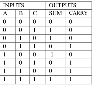
INPUTS OUTPUTS
A B SUM CARR
0 0 0 0
0 1 1 0
1 0 1 0
Table_3:Truth Table of the Half Subtractor
C.Full Adder and the Full Subtractor using the proposed NR Gate:
By using two NR Gate the Full Adder and Fullsubtractor were designed. Inputs A and B is given to the NRG-1 and input C is given to the -NRG-2 . The Sum and Carry of Full Adder is taken from the NRG-2 gate Q and R output respectively.
Figure 5(e). The full adder and the full subtractor implementation using the proposed NR Gate
For the Full Subtractor, the Difference and Borrow is taken from the NRG2 gate Q and S output respectively.The Representation of FA and FS using NR Gate shown in figure 5(e).
Table_4: Truth Table of the Full Adder
Table_5: Truth Table of the Full Subtractor
VI. COMPARISON
Table For The Other Full Adders & The Proposed Full Adder Using NR Gate:[13]
Comparing to the existing one we can prefer for the new proposed adder because of its usage of less no. of gates and low optical cost and delay.
Table_6: Comparative Table
VI. SIMULATION AND THE RESULTS
CIRCUIT SIMULATION
The circuit is simulated using Optisystem Sofware
INPUTS OUTPUTS
A B DIFF BORR
0 0 0 0
0 1 1 0
1 0 1 1
1 1 1 0
INPUTS OUTPUTS
A B C SUM CARRY
0 0 0 0 0
0 0 1 1 0
0 1 0 1 0
0 1 1 0 1
1 0 0 1 0
1 0 1 0 1
1 1 0 0 1
1 1 1 1 1
INPUTS OUTPUTS
A B C DIFF BORR
0 0 0 0 0
0 0 1 1 1
0 1 0 1 1
0 1 1 0 1
1 0 0 1 0
1 0 1 0 0
1 1 0 0 0
1 1 1 1 1
Composition Gates Optical Cost
Delay
Toffli + Feynman 16+3 54 13Δ
TNOR + Feynman 16+3 38 8Δ
TNOR +Toffli 8+6 34 13Δ
[image:4.612.52.275.259.369.2] [image:4.612.95.248.460.600.2]Output for the circuit When A=101,B=110
Sum,Difference=011 Carry=100 Borrow=010
Similarly We can Simulate for the proposed Full adder.
VII. CONCLUSION
We conclude that for the design of optical reversible binary adder and Subtractor using the proposed NR gate can be very much beneficial in minimizing the optical cost and the delay along with number of ancilla inputs and garbage output. The all existing reversible gate implemented for Adder and Subtractor , we should change the input for either operation, but in this proposed reversible NR Gate we could take output of Half Adder , Half Subtractor ,Full Adder and Full Subtractor output without changing the input.
REFERENCES
[1] R. Landauer, “Irreversibility and heat generation in the computing process,”IBM J. Res. Develop., vol. 3, pp. 183–191, 1961.
[2] Bennett, C.H., “Logical reversibility of Computation”, IBM J.Research and Development, 17: pp. 525-532, 1973.
[3] B.Raghu kanth, B.Murali Krishna, M. Sridhar, V.G. Santhi Swaroop ―A DISTINGUISH BETWEEN REVERSIBLE AND CONVENTIONAL LOGIC GATES ‖, International Journal of Engineering Research and Applications (IJERA) ISSN: 2248-9622 www.ijera.com Vol. 2, Issue 2,Mar-Apr 2012, pp.148-151
[4] Hafiz Md. Hasan babu, Md. Rafiqu Islam, Ahsan Raja Chowdhary and Syed Mostahead Ali chowdhary “ Reversible logic synthesis for minimization of full adder ckt”, IEEE conference on Digital system design 2003,Enro-micro‟03, Belek,Antalya,Tarkey,2003,PP 50-54 [4] H
[5] H.Thapliyal and N. Ranganathan, ―Design of reversible sequentialcircuits optimizing quantum cost, delay and garbage outputs,‖ ACMJournal of Emerging Technologies in Computing Systems, vol. 6, no.4, Article 14, pp. 14:1–14:35, Dec. 2010.
[6] E. Fredkin and T. Toffoli, “Conservative logic,” International J. Theor. Physics, vol. 21, pp. 219–253, 1982. [13] Y. Huang and P. Kumar, “Fredkin gates in χ(2) microdisks via quantum.
[7] M. Mohammadi and M. Eshghi. On figures of merit in reversible and quantum logic designs. Quantum Information Processing, 8(4):297– 318, Aug. 2009.
[8] C. Taraphdara, T. Chattopadhyay, and J. Roy, “Mach-zehnder interferometer-based all-optical reversible logic gate,” Optics and Laser Technology, vol. 42, no. 2, pp. 249–259, 2010
[9] J. A. Smolin and D. P. DiVincenzo, “Five two-bit quantum gates are sufficient to implement the quantum fredkin gate,” Physical Review A, vol. 53, pp. 2855–2856.
[10] W. N. Hung, X. Song, G.Yang, J.Yang, and M. Perkowski, “Optimal synthesis of multiple output boolean functions using a set of quantum gates by symbolic reachability analysis,” IEEE Trans. Computer-AidedDesign, vol. 25, no. 9, pp. 1652–1663, Sept. 2006.
[11] D. Maslov and D. M. Miller, “Comparison of the cost metrics for reversible and quantum logic synthesis,” 0511008, 2006.
[12] A. K. Cherri and A. S. Al-Zayed, “Circuit designs of ultra-fast all-optical modified signed-digit adders using semiconductor optical amplifier and
mach-zehnder interferometer,” Optik - International Journal for Lightand Electron Optics, vol. 121, no. 17, pp. 1577 – 1585, 2010.
[13] All Optical implementation of high speed and low power reversible full adder using semiconductor optical amplifier based mach-zender interferometer Journal of Computer Science 10 (7): 1130-1134, 2014 ISSN: 1549-3636 © 2014 Science Publications.
AUTHORS
First Author – Theresal T is an Asst Prof (OG) in SRM University. She obtained B.E Degree in Xaviers Catholic College of Engineering and PG in A.C. Tech, Karaikudi. She has Presented Paper in Third IEEE International Conference on Communication and signal Processing titled on All Optical Basic Gates and XOR Gate Using SOA Based MZI also other paper titled Design All Optical Reversible Logic Gates. Rakesh.P ,Theresal.T, published a paper on ”Intellectual Power Generation Through Solar Energy”,IJRIT”issue no-2,volume no -2,April 2014. She is currently working on a project towards ‘ REVERSIBLE ALU’ ., Email: [email protected]
Second Author – Sathish K, is persuing his B.Tech degree under the department of ECE in SRM University. He presented a paper in an International Conference on AN OPTIMIZED IMPLEMENTATION OF ALL REVERSIBLE LOGIC GATE USING NEWLY DESIGNED ‘ALL GATE’. He is currently working on a project towards ‘ REVERSIBLE ALU’ . Email: [email protected]