International Journal of Emerging Technology and Advanced Engineering
Website: www.ijetae.com (ISSN 2250-2459, ISO 9001:2008 Certified Journal, Volume 4, Issue 9, September 2014)
Low Power Binary Floating Multiplier using Bypassing
Technique
Ekta
1, Yogesh Khandagre
2, Alok Dubey
3 1,2,3Trinity Institute of Research and Technology, Bhopal, India
Abstract— Floating point multiplication is used in many
digital signal processing (DSP) applications; this multiplication is costly in terms of area, delay and power consumption. Reduction in these parameters will greatly improve the performance of multiplier and this in turn will improve the performance of DSP systems. In this paper, a binary floating point multiplier is implemented using column bypass technique. The multiplier supports IEEE P754 standard, in this work IEEE P754 – 32 bit format is followed. Column bypass multiplier is used to reduce dynamic power consumption. The multiplier is implemented on Virtex 5-XC5VLX-3FF324 FPGA.
Keywords— Binary floating point multiplication, IEEE
P754 standard, dynamic power consumption, resource utilization, delay, column bypass technique, FPGA
I. INTRODUCTION
Floating point multiplication is the core process in any DSP application and optimizing the floating point multiplication process will improve the performance of overall application. Binary floating point multiplication is used in almost all the DSP applications that we are using today. IEEE has given a standard called IEEE P754 standard for floating point numbers, the two most commonly used formats are single precision format (32 bit) and double precision format (64 bit), in this work we have used single precision format for representing binary floating numbers. Figure 1 shows the single precision format. In single precision format first 23 bits (0 - 22) are used to represent mantissa, in binary floating point representation 1additional bit is concatenated as MSB in mantissa for normalization. Next 8 bits (23 - 30) are used to represent exponent, this exponent is biased to 127 so that the exponent never becomes negative. And the last bit (31) is used to represent sign; 1 for negative and 0 for positive numbers [1,2].
32 bits (0 - 31)
1 bit 8 bits 23 bits
Sign Exponent Mantissa
Figure 1. IEEE single precision format/32 bit format for binary floating point numbers.
A fixed point multiplication is required in implementing floating point multiplication, this fixed point multiplication can be implemented with many algorithms like Braun’s multiplier [3], shift and add multiplier [4], Vedic multiplier [5], Wallace tree multiplier [6], Booths algorithm [7], bypass techniques [8] and many more. In this work our focus was to reduce power consumption of our design so we have opted column bypass multiplication technique.
The paper is organized as follows: In section II previous work about floating point multiplication is discussed, in section III floating point multiplication algorithm is discussed along with its hardware implementation. Section IV will have details about column bypass technique and its effect on switching and dynamic power consumption. Section V contains details about behavioral simulation, synthesis report, delay report and power consumption report along with conclusion.
II. RELATED WORK
International Journal of Emerging Technology and Advanced Engineering
Website: www.ijetae.com (ISSN 2250-2459, ISO 9001:2008 Certified Journal, Volume 4, Issue 9, September 2014)
200 [5] Presents a multiplier which makes use of vedic technique, this design uses the Urdhva - triyakbhyam sutra to multiply two numbers, using this technique reduces the number of partial products generated during multiplication and this in-turn reduces the resource utilization of FPGA, this also reduces the latency as gate count reduces due to less hardware. [8] Suggested a column bypass multiplier, this multiplier is similar to an array multiplier but with lower power consumption, the design makes use of the fact that if any of the input bit is zero then the result of addition is same as the other bit to be added, hence in this method the full adders of that column is turned off and this in-turn reduces the dynamic power consumption of design. This design has lower power consumption than Braun’s multiplier with slight area overhead. In this work we have used column bypass technique to implement binary floating point multiplier; this technique reduces the dynamic power consumption of the target device (Virtex 5) by reducing the switching activity inside FPGA.
III. FLOATING POINT MULTIPLIER
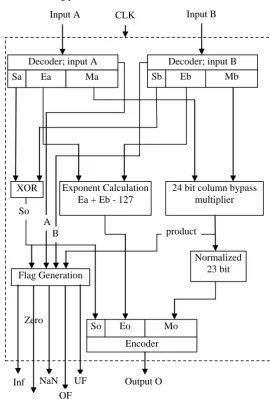
Figure 2 depicts the proposed binary floating point multiplier, in this work we have implemented multiplier with both Vedic multiplication technique and column bypass technique, it is found in results that column bypass technique is better in of dynamic power consumption with very small increase in latency.
As seen in figure 2 floating point multiplier can be portioned into following units
a. IEEE P754 decoder unit b. 24 bit multiplier
c. Exponent calculation unit d. Sign calculation
e. Flag generation unit f. IEEE P754 encoding unit
[image:2.595.309.580.157.557.2]a) IEEE P754 decoder unit: The standard representation of floating point number is
Figure 2. Proposed floating point multiplier architecture; single precision format
Zero
XOR Exponent Calculation Ea + Eb - 127
24 bit column bypass multiplier
Sa Ea Ma Sb Eb Mb
Decoder; input A Decoder; input B
So Eo Mo
Encoder
Normalized 23 bit Flag Generation
So A
B product
Input A Input B
Output O Inf NaN
OF UF
International Journal of Emerging Technology and Advanced Engineering
Website: www.ijetae.com (ISSN 2250-2459, ISO 9001:2008 Certified Journal, Volume 4, Issue 9, September 2014)
( ) ( )
The biased exponent E is original exponent e + 127 and the fraction M = )
The decoder unit extracts the three information from the incoming packet of 32 bits, first sign information S which is bit 31 refer figure 1. Second, it extracts exponent information E which lies between bits 30 - 23. And last the mantissa from bits 22 - 0. Additional 1 is concatenated at the MSB location in mantissa for normalization and normalized mantissa M is produced. Here 2 decoders are used one for input A and other for input B. we get Sa, Ea and Ma from decoder A and Sb, Eb, Mb form decoder B. b) 24 bit multiplier: A fixed point multiplication is
required to perform floating point multiplication. Many fixed point multiplication algorithms are available in literature. Here our focus was to reduce power consumption of multiplier so we have chosen column bypass technique. This technique is will be explained in detail in section III.
c) Exponent Calculation unit: In IEEE P754 single precision format the exponents is biased to 127. To calculate the final output exponent first we need to add the two exponents Ea and Eb obtained from decoder unit and then subtract 127.
d) We get Sa and Sb from decoder, one is used to represent negative number and zero is used to represent positive number. Output sign can be obtained by simply XORING the two sign bits Sa and Sb.
e) Flag generation unit: Five different flags are generated namely; InF (infinity), Zero, NaN (not a number), OF (overflow) and UF (underflow) see figure 2. The various conditions which affect these flags are listed below.
i. E = 255 and M ≠ 0, then NaN
ii. E = 255 and M = 0, then InF
iii. If 0 < E < 255, then number is
( ) ( )
iv. If E = 0 and F ≠ 0, then
( ) ( )
v. If E = 0 and M = 0, then Zero
vi. If some information is lost in truncation of mantissa then overflow and negative of overflow is underflow.
f) IEEE P754 Encoding unit: So, Eo and Mo are encoded to produce the output result format. The 48 bits from multiplier are truncated to most significant 24 bits. Then
g) The MSB is also truncated to produce the 23 bit
Consider two floating point numbers A = -19.0 and B = 9.5, there normalized binary representation are A = – 1.0011x 24 and B = 1.0011 X 23. IEEE representation of operands is:
[image:3.595.310.554.127.410.2]
Figure 3: Algorithm for binary floating point multiplication
Packet sign Exponent Mantissa
A = 1 10000011 00110000000000000000000 B = 0 10000010 00110000000000000000000
Here, MSB of both packets A and B shows the sign bits Sa (12) and Sb (02) respectively, the output sign is
calculated by XORING Sa and Sb (12 XOR 02), so output
sign bit So will be 12 here. The exponents are biased to
12710. Ea is 410 + 12710 = 13110 (10000011b) and Eb is 310
+12710 = 13110 (100000102). The output exponent is
calculated by adding both exponents and then subtracting the biased value which is 12710 in single precision format,
so output exponent will be 13210 + 13110 - 12710 = 13610
(100010002). To calculate the output mantissa first, the
two mantissa are concatenated with 12 and mantissa for
multiplication are formed:
Ma = 100110000000000000000000
Mb = 100110000000000000000000
Now multiplication of mantissa is accomplished using a 24 bit multiplier and 48 bit product is formed:
0101101001000000000000000000000000000000000000 00
Now the most significant 1 is truncated and least significant 24 bits are also truncated to form the output mantissa Mo.
01101001000000000000000.
Now the output packet is formed by encoding So, Eo and Mo:
Packet sign Exponent Mantissa
O = 1 10000110 01101001000000000000000
Algorithm for Binary floating point multiplication
1. Extract Sa, Ea, Ma, Sb, Eb, Mb by decoding the incoming packets.
2. So <= Sa XOR Sb 3. Eo <= Ea + Eb – 127 4. Product <= Ma * Mb
5. Truncate product and the normalize to produce Mo
6. Generate appropriate flags InF, NaN, Zero, OF,UF.
International Journal of Emerging Technology and Advanced Engineering
Website: www.ijetae.com (ISSN 2250-2459, ISO 9001:2008 Certified Journal, Volume 4, Issue 9, September 2014)
202 The result can be understood as: A X B = -19.0 X 9.5 = 180.5 = -1.01101001 X 2134-127 = (-1.0110100.1)2 =
(-180.5)10 [9].
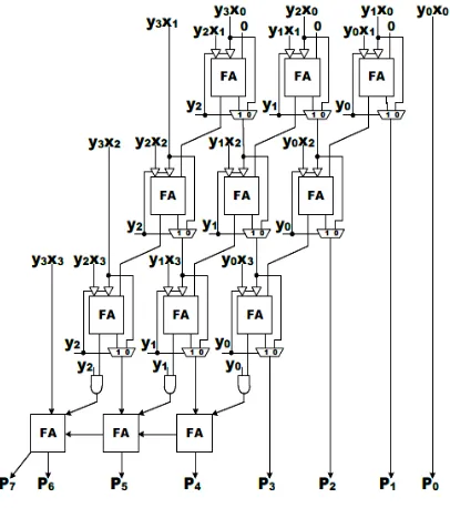
IV. COLUMN BYPASS MULTIPLIER DESIGN
[image:4.595.65.268.266.495.2]The performance of fixed point multiplier unit dominates the performance of overall floating point multiplier unit. In this work our focus was to reduce the dynamic power consumption of design so we have opted column bypass multiplier.
Figure 3:Column bypass multiplier
Consider an array multiplier [3], which has many full adders it, when one of the two bits is zero the resultant sum, is same as the other bit. In simple array multiplier this zero is added and this causes unwanted switching inside the full adder. Bypass techniques [10], uses this property of full adder and suppress unwanted switching, this switching is the cause of dynamic power consumption so by reducing this switching dynamic power consumption can be reduced. Column bypass multiplier as shown in figure 3 is a bypass method which is used to reduce unwanted switching of full adder and this in-turn reduces dynamic power consumption.
In our design we have used a 24 bit column bypass multiplier. The advantage of choosing this architecture is suppressing unwanted switching inside the multiplier unit. The column addition can be bypassed, when the bit of multiplicand, yi is 0, 0 ≤ i ≤ n – 2. This causes all partial
products yixi = 0, 0 ≤ j ≤ n – 1, thus all full adders can be
disabled in the ith column. This reduces the unwanted switching and in turn reduces the dynamic power consumption [8].
V. RESULTS AND CONCLUSION
International Journal of Emerging Technology and Advanced Engineering
Website: www.ijetae.com (ISSN 2250-2459, ISO 9001:2008 Certified Journal, Volume 4, Issue 9, September 2014)
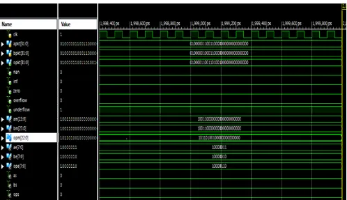
[image:5.595.60.558.130.417.2]Figure 4: Behavioral Simulation of binary floating point multiplier
TABLE 1 Design Summary
Parameters Our Design Vedic
Device Virtex 5 Virtex 5 Power Consumption 23mW 31mW
Time Delay 5.745ns 5.741ns Number of BUFGs 1 1 Number of OLOGICs 33 9 Number of LUTs 859 710 Number of Slices 299 269
Number of Slice
Registers 0 406 Number of Slice LUT
FF Pairs 859 791 Number of IO 102 99 Power Delay Product 132.135pJ 177.97pJ
NA: Not Available
As we can see from the table 1 that power consumption is reduced to 23mW from 31mW as compared to binary floating point multiplier using Vedic multiplication technique [5]. This is because of the use of column bypass multiplier. A small increase in delay is observed this is because of the use of complex multiplier. But overall performance of the device was improved. Also Number of slice registers used in our design is zero as compared to Vedic technique which uses 406, so the overall resource usage comparable.
REFERENCES
[1] IEEE 754-2008, IEEE Standard for Floating-Point Arithmetic, 2008.
[2] Brian Hickmann, Andrew Krioukov, and Michael Schulte, Mark Erle,”A Parallel IEEE 754 Decimal Floating-Point Multiplier,” In 25th International Conference on Computer Design ICCD, Oct.
2007.
[3] R Anitha and V Bagyaveereswan “Braun's Multiplier Implementation using FPGA with Bypassing Techniques” International journal of VLSI design and communication system (VLSICS) vol2, no 3. September 2011.
[4] C.N. Marimuthu, P. Thangaraj and Aswathy Ramesan “Low power shift and add multiplier design” International jaournal of computer scince and information technology 2.3 (2010) 12-15.
[5] Aniruddha Kanhe, Shishir Kumar Das and Ankit Kumar Singh “Design and implementation of floating point multiplier based on vedic multiplication technique ” International Conference on communication, information & computing technology (ICCICT), oct 2011 IEEE.
[6] Fadavi-Ardekani “M*N Booth encoded multiplier generator using optimized Wallace trees” IEEE transactions on very large scale integration (VLSI) systems, vol1 issue 2, june 1993 pp 120-125. [7] Shanbang N.R. “Parallel implementation of a 4*4 bit multiplier
using a modified Booth’s algorithm” IEEE journal of solid stste circuits vol 23 issue 4 Aug 1988 pp 1010-1013.
[8] Ming-chen Wen, Sying-Jyan Wang and Yen-Nan Lin “Low power multiplier with column bypassing” Internation symposium on circuits and systems, may 2005 vol. 2 pp 1638-1641.
International Journal of Emerging Technology and Advanced Engineering
Website: www.ijetae.com (ISSN 2250-2459, ISO 9001:2008 Certified Journal, Volume 4, Issue 9, September 2014)
204
[10] Jun-ni Ohban, Moshnyaga V.G. and Inoue K “Multiplier energy reduction through bypassing of partial products” 2002 Asia-pacific conference on circuits and systems, vol. 2 pp 13-17.
[11] Kavita Khare, R.P.Singh, Nilay Khare,”Comparison of pipelined IEEE-754 standard floating point multiplier with unpipelined multiplier” Journal of Scientific & Industrial Research Vol.65, pages 900-904 November 2006.
[12] Anna Jain, Baisakhy dash and Ajit Kumar Panda “FPGA design of fast 32-bit floating point multiplier unit”.
[13] Manish Kumar Jaiswal and Ray C.C. Cheung “Area-Efficient FPGA implementation of quadruple precision floating point multiplier” 26th International parallel and distributed processing
symposium workshop and Phd forum, IEEE computer society, 2012.