DESIGN AND SIMULATION OF RECONFIGURABLE
MULTIWAVELENGTH VCSEL USING MEMS
1M.SHANMUGAPRIYA, 2M.MEENAKSHI
1Research Scholar, Department of Electronics and communication, Anna University, INDIA 2Professor, Department of Electronics and communication, Anna University, INDIA
E-mail: [email protected], [email protected]
ABSTRACT
This paper describes the novel structure of the multi wavelength reconfigurable Vertical Cavity Surface Emitting Laser (VCSEL) with tunable Fabry Perot cavities. This device is designed to operate in the C band. The tunability is achieved by varying the cavity length of the filter using electrostatic actuator. The cavity length of the filter is varied to resonate at discrete wavelengths. The cavity length variation is achieved by using MEMS based electrostatic actuator. The active layer of VCSEL is modeled with three quantum wells, and is sandwiched between the DBR mirrors to give high gain. The tunable portion consists of an array of four filters to give different wavelengths. The detail analysis of the filter is carried out and the performance is analysed using Intellisuite software.
Keywords: VCSEL, Fabry Perot Filter, MEMS, Electrostatic Actuator, Tunable Filter
1. INTRODUCTION
The MEMS technology integrated with photonics has been one of the essential techniques in the fabrication of optical device. The advantages of this fusion technology give good optical performance, reconfigurabilty, tunablity, CMOS integration with optical device, batch processing and thereby reducing the cost of the device [8]. The all optical network nowadays has a very high demand in the telecommunication field. In recent years, research on VCSELs has shifted from short-wavelength (850 to 980 nm) GAAs-based [1] materials to InP-based [2], GaN-based [3] and GaSb-based [4] materials to fabricate long wavelength devices [5], fixed wavelength devices [6], tunable lasers [7] and multiwavelength arrays [8]. Intensive research has been made in the area of long wavelength tunable VCSEL with great progress. The VCSEL has tremendous advantages such as vertical emission from the substrate, low power consumption, circular beam profile, very low threshold operation, wavelength and thresholds are relatively insensitive with temperature variation, dynamic single mode operation, high speed modulation, long device lifetime due to the completely embedded active region and passivated surfaces and high power conversion efficiency. Easy coupling to the single or multi-mode fibers, mass fabrication, densely packed and precisely arranged two-dimensional (2-D) laser arrays can be formed and easy probe testing in the
die itself is possible [9]. The tunable VCSEL with MEMS technology gives a promising idea of designing the long wavelength VCSEL. The MEMS technology gives continuous tuning range, low power and the low cost of manufacturing also. The 680nm and 900 nm are fabricated using GaAs [10]. Still designing a device structure that can be manufactured with as low cost as 850-nm GA As-based VCSELs remains a major challenge. For the telecommunication application the 10 Gbps speed should be achieved using long wavelength VCSEL with direct modulation.
in data transmission over the optical fiber [13]. The longer wavelength VCSEL is fabricated using InP. In the recent past a lot of research has focussed on designing a low cost InP-based long wavelength VCSEL. This paper describes all optical device, namely the tunable VCSEL laser combined with Fabry filter or Bragg filter. In designing the VCSEL, the InP multiple quantum wells are sandwiched between AlGaAs DBR mirrors with alternate low and high refractive index. The tuning portion of the VCSEL is basically used to shift the output wavelength to the desired wavelength. The tuning may be continuous or discrete. The continuous tuning will be affected by the RC parasitic. But the surface micromachining will help the device separating the tuning part from the VCSEL. So the parasitic effects may be avoided. The frequency shift from the fixed wavelength output or in other words the tuning may be achieved by varying the gap between the reflecting mirrors. The gap will decide which wavelength the VCSEL should emit. The tunability can be achieved either by using the Bragg or Fabry perot filtering concept. In the Bragg filter the tunablity is achieved by the changing the grating period. The Bragg wavelength is calculated using 2ᴧneff=λB.Where ᴧ is the grating
period and neff is the effective refractive index of the
medium. The Fabry Perot filter consists of two parallel, highly reflecting mirrors separated by a small distance ’d’ to form a resonant optical cavity. The micromachining technique gives a new approach to the fabrication of Fabry-Perot tunable filters. The length of the Fabry perot filter is varied by varying the gap between the mirrors.
In this work the Fabry-Perot cavity adjustment is used for tuning the gap between the mirrors. Section I provides the introduction and the related work done. Section II describes the structure of tunable VCSEL. The structure of tunable four array filter is is discussed in section III. The obtained results are presented in section IV.
2. TUNABLE VCSEL
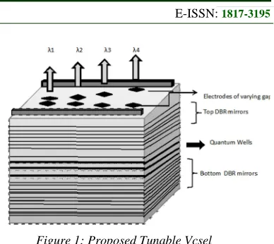
[image:2.612.330.524.72.245.2]The novel optical device such as filter and laser are coupled to form a novel reconfigurable tunable VCSEL structures which are shown in Figure 1. The design of a novel tunable structure with cantilever beams and parallel plate actuator has been proposed. The Fabry Perot concept can be achieved using the cantilever beam or parallel plate actuators. In both the cases, the electrostatic actuation can be used.
Figure 1: Proposed Tunable Vcsel
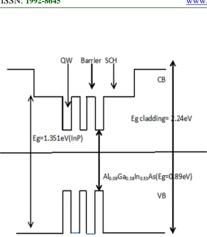
The active region comprises of multiple quantum wells with alternating thin layers of wider and narrower band-gaps. The stack of band gaps creates a series of potential wells. As the dimensions of the potential wells are reduced to the order of 10 nm, the movement of electrons is restricted inside the potential well and quantum effects are more prominent. The quantum well effect makes it possible to tailor the shapes of the gain function of a VCSEL so that it is peaked at a specified frequency[13]. Large tuning-range and high-speed operation can be achieved by using highly strained quantum wells, thereby increasing the differential gain and reducing the threshold carrier density. The InAlGaAs/InP active cavity quantum well is combined with wafer-fused AlGaAs/GaAs DBR mirrors.In this proposed structure, the design values of VCSEL is based on the design proposed in [2], [9] and [11]. It contains three QWs of Al0.09Ga0.38In0.53As separated by InP barriers as the
active layers for 1550nm operation.
Figure.2 shows the active layer of the VCSEL consisting of two cladding layers of Al0.6Ga0.4As. The cladding and active layer
materials are separated by two separate confinement heterostructure (SCH) layers of InP. On the top and bottom of 3QW cavity active region, upper and lower Distributed Bragg Reflector (DBR) stacks are formed. The energy level of the quantum well is designed with the following equation [1]
Eg = 1.35+ (0.642+0.758x)x+
(0.101y-1.101)y-(0.28x-0.109y+0.159) xy . (1)
where x and y represents the mole fraction of the material. The quantum well materials chosen to have the band gap energy of 0.89eV. The Eg of InP
barrier material, is calculated as 1.351eV and the Eg
Figure :2 Quantum Well Used In The Active Layer Of VCSEL .
Values of a number of parameters are obtained from different published sources [13].. The lattice constant of QW and barrier material is 5.869. The active region of the VCSEL is separated by two upper and lower DBR stacks. The upper 26 DBR mirrors are designed to get 96.1% reflectivity and the lower 60 DBR mirrors are designed to get 99.9% reflectivity. The reflectivity is calculated by using the formula.
R= ቈଵି
భ మ
మౣ
ଵାభ మ
మౣ ଶ
(2)
Where R = Reflectivity of the mirrors n1= refractive index of AlGaAs
n2= refractive index of InAlGaAs
m= no of mirrors
The current is injected through the upper p-type contact and the lower n-type contact is connected with the substrate.
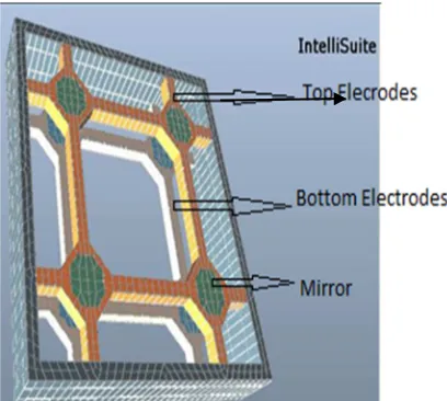
3. TUNABLE FOUR ARRAY FILTER
The tunability is achieved by using the Fabry Perot filter. The four arrays Fabry Perot filter comprises of two parallel, highly reflecting mirrors separated by a small distance’d’ to form a resonant optical cavity is shown in Figure.2. A very high mirror reflectivity is required to obtain good isolation of adjacent channels. The Fabry Perot filter exhibits a peak transmittance at wavelengths
which resonate within the cavity, with transmittance rapidly falling away on either side of the resonant wavelengths. If no phase change is present in the mirrors, the resonant wavelengths are given by λ = 2d/m where m is an integer known as the order of the peak. The power transfer function T(f) is the fraction of input light power that is transmitted by the filter [14].
Tf
ሺଵିିୖሻమሺଵିୖሻమ
ାୖሾଶ ୱ୧୬ሺଶதሻሿమ (3)
where A = Absorption loss of each mirror, R = Reflectivity of each mirror, τ =d/c = one way propagation time c=velocity of light
λ= wave length,
n=Refractive Index of cavity.
The resonant condition of the optical cavity (d=mλ/2) is changed dynamically, by moving one of the mirrors. This Fabry Perot filter is designed to have the tunability in C-Band from 1520nm to 1550nm [15]. The initial cavity length of the filter is selected using its power transfer function. The power transfer function T(f) of the Fabry Perot filter is modeled in MATLAB by assuming zero absorption loss of the mirrors. The power transfer function is maximum, when the cavity length of the resonator d= mλ/2. High tuning range can be achieved when the filter operates in first order mode. So, the initial cavity length is chosen as 775nm for filtering a wavelength of 1550nm. The sharp response of the Fabry Perot filter can be obtained when the reflectivity R of the mirrors is high. When the reflectivity of mirror is 95%, highly sharp response can be observed. For R=35%, the sharpness of the filter response is moderate and for R=5%, a very low sharpness in its power transfer function can be observed.
(FSR) and the finesse (F). The FSR defines the spectral distance between two consecutive interference peaks, while finesse (F) is the FSR divided by the full width at half maximum of the interference peaks. FSR indicates the spectral tunability of the Fabry Perot device, while F specifies its spectral resolution. The Finesse of a Fabry Perot cavity is a function of fabrication imperfections and the reflectance of the mirrors. Tunable MEMS-based Fabry Perot filter is fabricated by using inexpensive batch processing micromachining process and hence is a suitable choice for integrating with the VCSEL.
[image:4.612.90.294.265.448.2]
Figure 3: Tunable Section In Fabry Perot Filter Array
The parallel plate actuator structure for varying the gap between the Fabry Perot filter is simulated using Intellisuite. Extensive analyses are carried out in finalizing the materials for the parallel plate actuator . The materials compared in this structure are Silicon di oxide (Sio2), Silicon
Nitrite (Si3N4) and poly silicon. It has been found
that Sio2 is the suitable material for the design of
Fabry Perot filter. Materials used are Silicon_bulk_general for the fixed supporting beams, Alluminium_bulk_general for the electrodes, Glass_Hoya_Sd2 for the reflecting mirrors. All the faces of the bottom electrodes, supporting beams are fixed. All the faces of the electrode and mirror in top side are made as movable. In the Intellisuite TEM analysis, a voltage range of 0-to-9V is applied to the fixed electrode in bottom layer and 0V is applied to the free electrode in top layer. Initial gap between the mirrors is taken as 775nm. Due to the electrostatic force of attraction the free electrode is moved down towards the fixed electrode. The free electrode can be
brought back to its original position when the voltage is removed, if an appropriate mechanical design is used. The voltage applied to the electrodes is calculated by using the equation (4)
d= ଶఢ
య
௩మ
ாௐ௧యሺ బିௗሻమ
(4)
Where g0 = initial air gap between the mirrors,
d = displacement to be achieved, V = voltage to be applied,
E = young’s modulus of the electrode material,
A = the area of the electrode.
L, W, t= length, width, and thickness of the electrodes respectively [7].
The pull in voltage defines the growth of the electrostatic force becoming dominant over the increasing mechanical restoring force and the upper electrode quickly pulls into the bottom electrode. To avoid the collapse between the electrodes the pull in voltage is calculated using the equation
Vpi=
଼బయ
ଶఢ (5)
Where k= ாௐ௧
య
ସయ
k = spring constant of material
E = young’s modulus of the electrode material, A = the area of the electrode.
L, W, t = length, width, and thickness of the electrodes respectively.
Beyond this Vpi the upper electrode is
suddenly pulled down by the lower electrode. Hence the maximum displacement between the electrodes will be corresponding to that of Vpi.
4 RESULTS AND DISCUSSION
The VCSEL is designed with active region having 3 quantum wells. The active layers of VCSEL are sandwiched between the DBR mirrors. The optimal number of mirrors is selected based on the reflectivity. The variation of number of mirror
stacks with reflectivity is shown in Figure 4. It is observed that the number of mirrors is found to be
Figure 4: Reflectivity Verses Number Of Mirrors.
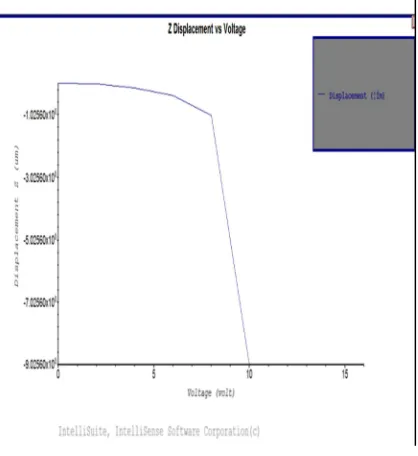
The tunable four array filter is modeled using Intellisuite and is shown in figure 3. The TEM analysis in the intellisuite software is carried out to determine the pull in voltage. The variation of displacement values obtained for different values of voltage is shown in Figure 5. It is found that the displacement reduces drastically at 9 volts. Hence the pull in voltage is fixed at 9v.
.Figure 5: Pull In Voltage
The simulation for the structure shown is done by considering different materials such as sio2, si3n4, polysilicon for the plates. The displacements values(d) and their corresponding wavelengths(λ)
[image:5.612.324.503.374.557.2]for different voltages applied are compared for these materials and are presented in Table 1.
Table 1: Comparison Of Materials
It is found that Sio2 is the best insulator as it provides good isolation of MEMS structure when compared to other materials and could yield 1556nm and the comparison is shown in the figure 6.
The simulation has been carried out for the designed length and breadth, by varying the plate thickness from 2µm to 5 µ m. It is observed that as plate thickness increases displacement decreases and the results are tabulated in the Table 2.
Figure 6: Comparison Of Materials For The 1556 Nm
Table 2: Comparison Of Electrode And Mirror Thickness
V (v)
Sio2 Si3n4 Polysilicon
d (µm)
λ
(µm) d (µm)
λ
(µm) d (µm)
λ
(µm)
5 3.34 1.56 .8212 1.49 1.202 1.6 10 4.15 1.56 1.847 1.57 2.598 1.56
Vol tage (v)
Sio2
displacement (µm)
Si3n4
displacement (µm)
Polysilicon displacement
(µm)
t=2µm t=5µm t=2µm t=5µm t=2µm t=5µm
1 .04 3.3 9.8 .82 2.1 2.5
3 .01 1.665 4.3 .40 8.2 .37
5 .01 .809 2.7 .02 5.3 .48
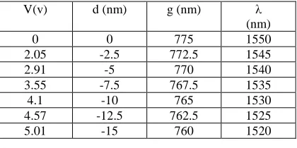
[image:5.612.91.300.377.605.2]To obtain the desired wavelength range of the tunable VCSEL in the range of C band , the voltage applied is varied from 0 to max of pullin voltage of 9v. The displacements for this wavelength range are determined for the varying voltages.The corresponding final gap are calculated and these values are presented in Table 3.
Table 3: Intellisuite Simulated Results That Show Voltage Vs Displacement Values When The Initial Gap Between
Electrodes Is 775nm
The optimal values of voltage(V), displacement(d) and final gap(g) are determined to yield the required wavelength range(λ) of 1520 to1550 nm
5. CONCLUSION
In this paper a novel reconfigurable multi wavelength tunable VCSEL structure based on MEMS is proposed to operate in the C band. The substrate and design values are identified for the proposed structure and simulated using Intellisuit the simulated results shows the tuning over 1520 to 1550 nm. The surface micro machining process gives the advantages of batch processing, thereby indicating the possibility to realize, a low cost reconfigurable all optical VCSEL.
REFRENCES:
[1] Yi Rao, “InP Based Long Wavelength VCSEL using High Contrast Grating”,Eecs
Department University Of California,
Berkeley Technical Report No. Ucb/Eecs 2012-261,December 14,2012
[2] M. Muller, W. Hofmann, T. Grundl, M. Horn, P. Wolf, R. D. Nagel, E. Ronneberg, G. Bohm, D. Bimberg and M. C. Amann, "1550-nmHigh-Speed Short-Cavity VCSELs," IEEEJournal of Selected Topics in
Quantum Electronics, vol. 17, no. 5, pp. 1158-1166, 2011.
[3] J. M. Redwing, D. A. S. Loeber, N..Anderson, M. A. Tischler and J. S. Flynn, "An optically pumped GaN–AlGaN vertical cavity surface
emitting laser," Applied Physics Letter, vol. 69, no. 1, 1996.
[4] A. Bachmann, K. Kashani-Shirazi, S. Arafin and M. C. Amann, "GaSb-Based VCSEL With Buried Tunnel Junction for Emission Around 2.3 µm," IEEE Journal of Selected
Topics in quantum Electronics, vol. 15, no. 3, pp. 933-940,2009.
[5] W. H. Hofmann, ``P. Moser, P. Wolf, A. Mutig, M.Krohand.Bimberg,"44Gb/sVCSELopticalin
terconnects," in OFC, Los Angeles,
California, USA, 2011.
[6] M. C. Y. Huang, Y. Zhou and C. J. Chang- Hasnain, "A nanoelectromechanical tunable laser," Nature Photonics, vol. 2, pp. 180-184, 2008.
[7] C. Chang-Hasnain, J. Harbison, C.-E. Zah, M. Maeda, L. Florez, N. Stoffel and T.-P. Lee, "Multiple wavelength tunable surface-mitting laser arrays," IEEE Journal of uantumElectronics, vol. 17, no. 6, pp. 1368-1376 ,1991.
[8] T. Wipiejewski, J. Ko, B. Thibeault and .Coldren, "Multiple wavelength vertical-cavity laser array employing molecular beam epitaxy regrowth," Electronics Letters, vol. 32, no. 4, pp. 340-342, 1998.
[9] K. Iga, "Surface-emitting laser-its birth and generation of new optoelectronics field,"
IEEE Journal of Selected Topics in Quantum Electronics, vol. 6, no. 6, pp. 1201-1215,
2000.
[10] S. Jatta, B. Kogel, M. Maute, K. Zogal, F. Riemenschneider, G. Bohm, M.-C. Amann and P.Meisner, "Bulk-micromachined VCSEL At 1.55 um with 76-nm single-mode continuous tuning range," IEEE Photonics
Technology Letters, vol. 21, no. 24, pp. 1822- 1825, 2009.
[11] Julien Boucart, Member, IEEE, Rajiv Pathak, Dongxu Zhang, Mario Beaudoin, Peter Kner, Decai Sun,Robert J. Stone, Rashit F. Nabiev, and Wupen Yuen, Member, IEEE “Long Wavelength MEMS Tunable VCSEL With InPAlGaAsBottomDBR”IEEEphotonicsTech
nology Letters, Vol. 15, No. 9, Pp.1186-1185, 2003.
[12] Yut Aka Onishi*, Nobuhiro Saga, Kenji Koyama, Hideyuki Doi, Takashi Ishizuka, Takashi Yamada, Kosuke Fujii, Hiroki Mori, Jun-Ichi Hashimoto, Mitsuru Simazu, Akira Yaaguchi And Tsukuru Katsuyama,ǁ “Long- Wavelength Gainnas Vcsel With Buried Tunnel Junction Current Confinement
V(v) d (nm) g (nm) λ
(nm)
0 0 775 1550
2.05 -2.5 772.5 1545
2.91 -5 770 1540
3.55 -7.5 767.5 1535
4.1 -10 765 1530
4.57 -12.5 762.5 1525
Structureǁ”, Sei Technical Review Number 68
April 2009.
[13] Tamal Roy, Avijit Das, Sujan Howlader, Md. Ronok Hasan Rubel and Rinku Basak,” Design and Performance Analysis of a 1550nm Al0.09Ga0.38In0.53As/InP MQW VCSEL by Varying Current”International
Journal Of Multidisciplinary Sciences And Engineering, Vol. 4, No. 2, February 2013.
[14] David Hays, Anis Zribi, ShankarChandrasekaran, Shivappa Goravar,Sandip Maity, Leonard R. Douglas, Kevin Hsu, and Ayan Banerjee and Ayan Banerjee "A Hybrid MEMS–Fiber OpticTunable Fabry–PerotFilter” Journal of
micro electro mechanical systems, vol. 19, no. 2, april 2010
[15]R.F.Wolffenbuttel, "State-of-the-art in integrated optical micro spectrometers”, IEEE
Transactions on Instrumentation and
Measurement, vol. 53, pp. 197-202, 2004.
[16] R. Le Dantec, D. Rondi, A. Spisser, R. Blondeau, J. Leclercq, P.Viktorovitch, T. Benyattou,C. Seassal and G. Guillot "Tunable microcavity based on InP-air Bragg mirrors,",