http://dx.doi.org/10.4236/ampc.2016.63003
How to cite this paper: Pham, K.N., Ta, K.H.T., Nguyen, L.T.T., Tran, V.C. and Phan, B.T. (2016) Surface Mapping of Resistive Switching CrOx Thin Films. Advances in Materials Physics and Chemistry, 6, 21-27.
http://dx.doi.org/10.4236/ampc.2016.63003
Surface Mapping of Resistive Switching
CrO
x
Thin Films
Kim Ngoc Pham
1*, Kieu Hanh Thi Ta
1, Lien Thuong Thi Nguyen
2, Vinh Cao Tran
3,
Bach Thang Phan
1,31Faculty of Materials Science, University of Science, Vietnam National University, Ho Chi Minh City, Vietnam 2Faculty of Resources and Environment, Thu Dau Mot University, Binh Duong City, Vietnam
3Laboratory of Advanced Materials, University of Science, Vietnam National University, Ho Chi Minh City, Vietnam
Received 7 February 2016; accepted 8 March 2016; published 11 March 2016
Copyright © 2016 by authors and Scientific Research Publishing Inc.
This work is licensed under the Creative Commons Attribution International License (CC BY). http://creativecommons.org/licenses/by/4.0/
Abstract
In this work, we investigated resistive switching behavior of CrOx thin films grown by using
sput-tering technique. Conventional I-V measurements obtained from Ag/CrOx/Pt/Ti/SiO2/Si structures
depict the bipolar switching behavior, which is controlled by formation/dissolution processes of Ag conducting filaments through electrochemical redox reaction under external electric field dri-ven. Conductive atomic force microscopy (C-AFM) technique provides the valuable mapping im-ages of existing Ag filaments at low resistance state as well as the characteristics of filament dis-tributions and diameters. This study also reveals that where the higher amplitude of topography is, the easier possibility of forming conducting filament paths is on CrOx surface films.
Keywords
Resistive Switching, Chromium Oxide, C-AFM, Surface Mapping, Metal Filament
1. Introduction
Resistance switching random access memory (RRAM) is a nonvolatile memory that works by changing resis-tance across the dielectric material layer referred to as a memristor. RRAM offers a variety of advantages such as fast write/erase speed, high integrated density, long retention and low power comsumption [1] [2]. Various models have been proposed to explain the resistance switching mechanisms as early as the 1960s, distributing
*
into two typical models including filamentary-controlled type and interface-controlled type [3]. However, these mechanisms still remain doubtful now; therefore, promote intensively scientists to give efforts finding evidences to illustrate such models.
Mechanism of filamentary-controlled type relates to the formation and rupture processes of tiny conducting paths through the memristor structure corresponding to low resistance state (LRS) and high resistance state (HRS), respectively. The observation of the filament is done by modern techniques, consisting of scanning tunneling microscopy (STM) [4] and conductive atomic force microscopy (C-AFM) [5], high-resolution EDX [6], high-resolution transmission electron microscopy (HRTEM) [7], electron energy loss spectroscopy (EELS) [8] analysis… Among them, C-AFM technique can provide effectively a range of morphological, electrical and mechanical information of a sample surface in nanoscale because C-AFM seems simple than others due to mea-suring electrical current in direct contact with the surface in an ambient condition without a conducting substrate. C-AFM has been readily used to analyze the electrical properties of gate oxides since the 1990s and provided much key information. It have been recently reported that direct observation of filament paths through memory environ-ment such as TiO2 [9], NiO [5], CuxO [10], graphene oxide films [11]… can be widely provided by C-AFM.
In this work, we have investigated the resistive switching effect of Ag/CrOx/Pt device prepared by using sputtering method. C-AFM technique is used to study the nanoscale electrical property as well as the switching mechanism of CrOx thin films. The surface mapping results show the distinct characteristics between LRS and HRS of device. Furthermore, the correlation between surface topography and capability of filament formation has been discussed in detail.
2. Experimental Procedures
The 100-nm-thick chromium oxide films were deposited by using the DC sputtering technique at room tem-perature, from metallic Cr target (99.95%) on Pt/Ti/SiO2/Si commercial substrate. The deposition process was executed under the total pressure
2 Ar O
P + of 7 × 10⁻³ Torr, and a gas mixture ratio of oxygen and argon,
2 2
O Ar O
P P + was fixed at 6%. The silver electrodes (Ag) were fabricated with a mask for top electrode patterning. To prepare samples for C-AFM measurement, 10-nm-CrOx/Ag configuration on glass has been fabricated. Pt coated probe tip of C-AFM plays a role of top electrode during detecting electrical current at contact mode.
Microstructure and surface morphologies of the films were obtained by D8 Advance (Bruker) X-ray diffrac-tometer (XRD) with Cu Kα radiation (λ = 0.154 nm) and scanning electron microscopy (SEM). Current-voltage (I-V) measurements were carried out on a probe station using a semiconductor characterization system (Keithley 4200 SCS). The voltage profile for the I–V measurement was 0 V −Vmax 0 V +Vmax 0 V. Topography images and current images during C-AFM scanning were detected by Veeco Dimension 3100 AFM system with DC sample bias.
[image:2.595.228.400.565.694.2]3. Results and Discussion
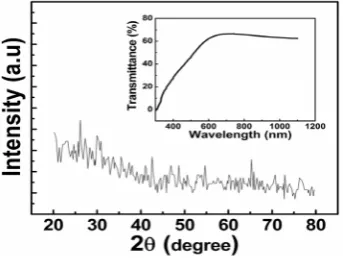
Figure 1 presents result of X-ray diffraction (XRD) analysis of chromium oxide film (100 nm) on glass sub-strate. It is showed that the structure was entirely amorphous without any crystalline peak. In this work, we have prepared CrOx thin film at room temperature with sputtering power as low as of 90 W and relative low oxygen
Figure 1.XRD pattern of 100 nm-thick CrOx thin film. Inserted image is
partial pressure (6%), so the structure of film remains primarily amorphous or poor cystallinity. This result is similar to that of other studies about chromium oxide thin films [12] [13]. Transmission spectrum of CrOx film in the wavelength rang of 400 - 1100 nm was inserted in Figure 1. It is a large variation of transmittance in the wavelength range lower than 600 nm. In contrast, the transmission is nearly constant and about 65% in the re-gion of 600 - 1100 nm.
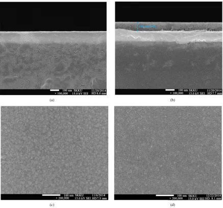
[image:3.595.95.533.286.693.2]Figure 2 shows SEM images of CrOx films prepared by reactive sputtering technique. Figure 2(a) and Fig-ure 2(b) exhibit cross-section images of Pt/Ti/SiO2/Si substrate and CrOx film on this substrate, respectively. It is found that thickness of CrOx film is approximately 100 nm and surface morphology is relative smooth. In ad-dition, the microstructure of film appears to be rather porous with many small holes inside. This feature is per-fectly suitable with the amorphous structure as shown in XRD from Figure 1. For I-V measurement, 100-nm- thick CrOx films was deposited on Pt substrate (Figure 2(c)). The grain size of this film is hard to examine due to unclear grain boundaries. For C-AFM measurement, CrOx film with only 10 nm in thickness was prepared on Ag bottom electrode (Figure 2(d)). In this case, particles distribute uniformly and grain size is smaller com-pared to that of 100-nm-thick CrOx films.
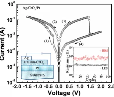
Figure 3 shows the typical current–voltage (I-V) curve of Ag/CrOx/Pt device investigated by applying elec-tric field process of 0 −1.5 V 0 2 V 0 V. The schematic of I-V measurement was inserted at the left
(a) (b)
(c) (d)
Figure 2. SEM images of CrOx thin film. Cross-section images of (a) Pt commercial substrate and (b) 100 nm-CrOx/Pt.
Figure 3.Typical bipolar resistive switching characteristics of Ag/CrOx/Pt devices. Sche-matics view of CrOx thin film for current-voltage measurement and endurance of device were inserted at the lower left and right corners, respectively.
corner of Figure 3. In this case, Pt bottom electrode was applied by electrical field whereas Ag top electrode was always grounded. CrOx films exhibit forming–free bipolar resistive switching bahavior in the range of −1.5 V 2 V with high endurance performance as seen in the insert at the right corner of Figure 3. For Ag/CrOx/Pt device, mechanism of resistive switching was proposed by the following electrochemical metallization
mechan-ism [14]. By sweeping the voltage from 0 −1.5 V, an electrochemical reaction occurs in the anode (Ag),
which oxidizes the Ag metal atoms to Ag ions. These metal ions Ag start from the top interface and easily drift through the amorphous CrOx films to connect the bottom electrode. At the Pt cathode, an electrochemical reduc-tion and an electro-crystallizareduc-tion of Ag occur. This process results in the formareduc-tion of an Ag filament and con-nects from the Pt electrode to the Ag top electrode. Once the connecting process completes, the switching from HRS to LRS happens (route 1). The LRS state remains during sweeping from −1.5 0 V. When applying the opposite polarity, the dissolution of the Ag filament occurs leading to the abrupt switching from LRS to HRS (route 3).
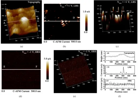
The direct observation of resistive switching mechanism of CrOx film has been justified by C-AFM. In our work, 10-nm-thick CrOxA/Ag/glass structure was prepared for the test. Here, Ag layer plays a role as a bottom electrode while Pt-coated tip of AFM system plays a role of top electrode (Figure 4(a)). Current mapping im-ages are performed in the specific scanning area of 1 × 1 µm2. For a virgin device, no leakage current is detected. This means that the initial state of device is HRS. When we apply a bias voltage of 0.5 V on Ag layer, there is no change in leakage current or the device till keeps HRS. With an increase of the bias voltage to 1 V, the lea-kage currents begins more clearly and device switchs to LRS state. There are appearances of randomly local bright pots which are high contrast to almost dark background of current map (in the above half part of Figure 4(b) and Figure 4(c)). This confirms that there is formation of silver conducting paths for current flow through metal oxide thin film under positive bias. Current compliance (Ic) is set up at 10 nA to avoid the permanent beakdown on device.
After completing the scanning with the down direction, the process is executed again with the up direction. For comparison, the latter scanning process performs only on the below half part of the mapping images. At this time, negative voltage of −1 V is applied on the Ag bottom electrode. It shows that conductive regions are com-pletely vanished and previous bright pots has been totally disappeared (the below half part of Figure 4(b) and Figure 4(c)). This means that by changing the polarity of the bias voltage, Ag metal can be dissolved at the end of filaments leading the rupture of conductive paths. Device turns back to HRS. These evidences affirm that the mechanism of resistive switching effect in CrOx films was controlled by formation/annihilation of conductive paths forming by electricalchemical redox of active metal electrode at the interfaces between CrOx layer and electrodes.
(a) (b) (c)
Figure 4.(a) Schematics of C-AFM measurement. Current mapping images in 2D (b) and 3D (c) including the above half
area with positive bias voltage of +1 V and the other half with negative bias voltage of −1V, respectively.
(a) (b) (c)
(d) (e) (f)
Figure 5.Morphology and corresponding current mapping images of 500 × 500 nm2 area of CrOx thin film. (a) 3D Surface
topography image of CrOx thin film. 2D and 3D Current mapping images of CrOx films at LRS ((b) and (c)) and HRS ((d)
and (e)), respectively. Corresponding plot of cross-section data of morphology and current images of AB, CD and EF lines, respectively (f).
[image:5.595.92.537.272.586.2]Contrary to the LRS, the current mapping is entirely homogeneous with very low current (~several picoamperes) in the HRS of device. It is clearly realized that all the conducting bridges were completely annihilated under re-versed bias voltage.
In addition, cross-section data at AB, CD and EF lines shows the close relation between surface morphology and leakage current value, as seen in Figure 5(f). The region with higher topography (middle of AB line) leads a larger current mapping (middle of CD line) at LRS. This feature can be explained following: During the C-AFM measurement, the tip contacts directly to surface films, so the high morphology areas on the CrOx film provide the high chance of contacting between tip and thin film surface. That leads the formation of conducting fila-ments is easier and the leakage current may be larger. On contrary, at the low morphology areas such as voids or pores, the tip hard approaches to these positions. Therefore, the possibility of forming filament is certain lower. Besides, it is found that diameter of filaments vary several tens of nanometers as in CD line. Diameter of fila-ments also reported smallest to be from several to tens of nanometers [17] [18]. The nanoscale resolution of me-tallic filaments is limited by geometry of commercial C-AFM tip. Moreover, the tip mechanically degraded in repeated scans under ambient conduction. Thus, the obtained diameter of filament herein seems to be diameter of a bunch of filaments. It is also clearly shown that the device with high density and small diameter of filaments would improve effectively the scalability of memory.
4. Conclusion
In summary, we propose the nonvolative memory device based on chromium oxide thin film and study behavior of resistive switching by using C-AFM technique. Current mapping images confirm that the electrochemical growth and dissolution of silver metallic filaments control the LRS and HLR of memory devices. Experimental results also suggest that the high amplitude of topography leading a high possibility of filament formation on the film surface. However, high fluctuation of filaments is still the crucial challenge to develop performance of memory devices based on resistive switching. Our work would be useful in understanding characteristics of fi-lament paths in transition metal oxide thin films.
Acknowledgements
This work was funded by National Foundation of Science and Technology Development of Vietnam (NAFOSTED- 103.02-2012.50). The authors gratefully acknowledge Prof. Jaichan Lee (Sungkyunkwan University, Republic of Korea) for supporting C-AFM analysis and Prof. Taekjib Choi (Sejong University, Republic of Korea) for valuable discussion.
References
[1] Waser, R. and Aono, M. (2007) Nanoionics-Based Resistive Switching Memories. Nature Materials, 6, 833-840.
http://dx.doi.org/10.1038/nmat2023
[2] Strukov, D.B. and Kohlstedt, H. (2012) Resistive Switching Phenomena in Thin Films: Materials, Devices, and
Appli-cations. MRS Bulletin, 37, 108-114. http://dx.doi.org/10.1557/mrs.2012.2
[3] Pan, F., Chen, C., Wang, Z., Yang, Y., Yang, J. and Zeng, F. (2010) Nonvolatile Resistive Switching Memories-Cha-
racteristics, Mechanisms and Challenges. Progress in Natural Science: Materials International, 20, 1-15.
http://dx.doi.org/10.1016/S1002-0071(12)60001-X
[4] Nayak, A., Tamura, T., Tsuruoka, T., Terabe, K., Hosaka, S., Hasegawa, T. and Aono, M. (2010) Rate-Limiting Pro-
cesses Determining the Switching Time in a Ag2S Atomic Switch. Journal of Physical Chemistry Letters, 1, 604-608.
http://dx.doi.org/10.1021/jz900375a
[5] Son, J.Y. and Shin, Y.-H. (2008) Direct Observation of Conducting Filaments on Resistive Switching of NiO Thin
Films. Applied Physics Letters, 92, 222106. http://dx.doi.org/10.1063/1.2931087
[6] Sakamoto, T., Lister, K., Banno, N., Hasegawa, T., Terabe, K. and Aono, M. (2007) Electronic Transport in Ta2O5
Re-sistive Switch. Applied Physics Letters, 91, 092110. http://dx.doi.org/10.1063/1.2777170
[7] Kwon, D.-H., Kim, K.M., Jang, J.H., Jeon, J.M., Lee, M.H., Kim, G.H., Hwang, C.S., et al. (2010) Atomic Structure of
Conducting Nanofilaments in TiO2 Resistive Switching Memory. Nature Nanotechnology, 5, 148-153.
http://dx.doi.org/10.1038/nnano.2009.456
[8] Park, G.S., Li, X.S., Kim, D.C., Jung, R.J., Lee, M.J. and Seo, S. (2007) Observation of Electric-Field Induced Ni
[9] Choi, B.J., Jeong, D.S., Kim, S.K., Rohde, C., Choi, S., Oh, J.H., Tiedke, S., et al. (2005) Resistive Switching
Me-chanism of TiO2 Thin Films Grown by Atomic-Layer Deposition. Journal of Applied Physics, 98. 033715.
http://dx.doi.org/10.1063/1.2001146
[10] Zhou, Q., Lu, Q., Zhang, X., Song, Y., Lin, Y.Y. and Wu, X. (2013) A Study of Copper Oxide Based Resistive
Switching Memory by Conductive Atom Force Microscope. Applied Surface Science, 271, 407-411.
http://dx.doi.org/10.1016/j.apsusc.2013.01.217
[11] Zhuge, F., Hu, B., He, C., Zhou, X., Liu, Z. and Li, R.-W. (2011) Mechanism of Nonvolatile Resistive Switching in
Graphene Oxide Thin Films. Carbon, 49, 3796-3802. http://dx.doi.org/10.1016/j.carbon.2011.04.071
[12] Qin, P., Fang, G., Sun, N., Fan, X., Zheng, Q., Chen, F., Zhao, X., et al. (2011) Organic Solar Cells with p-Type
Amorphous Chromium Oxide Thin Film as Hole-Transporting Layer. Thin Solid Films, 519, 4334-4341.
http://dx.doi.org/10.1016/j.tsf.2011.02.013
[13] Hong, S., Kim, E., Kim, D.-W., Sung, T.-H. and No, K. (1997) On Measurement of Optical Band Gap of Chromium
Oxide Films Containing Both Amorphous and Crystalline Phases. Journal of Non-Crystalline Solids, 221, 245-254.
http://dx.doi.org/10.1016/S0022-3093(97)00367-0
[14] Pham, N.K., Nguyen, D.T., Dao, B.T.T., Ta, K.H.T., Tran, V.C., Nguyen, V.H., Phan, T.B., et al. (2014) Different
Di-rections of Switching of Chromium Oxide Thin Films. Journal of Electronic Materials, 43, 2747-2753.
http://dx.doi.org/10.1007/s11664-014-3193-3
[15] Deleruyelle, D., Putero, M., Ouled-Khachroum, T., Bocquet, M., Coulet, M.-V., Boddaert, X., Muller, C., et al. (2013)
Ge2Sb2Te5 Layer Used as Solid Electrolyte in Conductive-Bridge Memory Devices Fabricated on Flexible Substrate.
Solid-State Electronics, 79, 159-165. http://dx.doi.org/10.1016/j.sse.2012.06.010
[16] Shang, D.-S., Shi, L., Sun, J.-R. and Shen, B.-G. (2011) Local Resistance Switching at Grain and Grain Boundary
Sur-faces of Polycrystalline Tungsten Oxide Films. Nanotechnology, 22, 254008.
http://dx.doi.org/10.1088/0957-4484/22/25/254008
[17] Ye, J.Y., Li, Y.Q., Gao, J., Peng, H.Y., Wu, S.X. and Wu, T. (2010) Nanoscale Resistive Switching and Filamentary
Conduction in NiO Thin Films. Applied Physics Letters, 97, 132108. http://dx.doi.org/10.1063/1.3494267
[18] Rosezin, R., Meier, M., Breuer, U., Kgeler, C. and Waser, R. (2011) Electroforming and Resistance Switching
Charac-teristics of Silver-Doped MSQ with Inert Electrodes. IEEE Transactions on Nanotechnology, 10, 338-343.