N A N O E X P R E S S
Open Access
Low-temperature poly-Si nanowire junctionless
devices with gate-all-around TiN/Al
2
O
3
stack
structure using an implant-free technique
Chun-Jung Su
1,2, Tzu-I Tsai
3, Horng-Chih Lin
2,4*, Tiao-Yuan Huang
2and Tien-Sheng Chao
3Abstract
In this work, we present a gate-all-around (GAA) low-temperature poly-Si nanowire (NW) junctionless device with TiN/Al2O3gate stack using an implant-free approach. Since the source/drain and channel regions are sharing onein situphosphorous-doped poly-Si material, the process flow and cost could be efficiently reduced. Owing to the GAA configuration and small volume of NW channels, the fabricated devices with heavily doped channels display superior switching behaviors and excellent immunity to short-channel effects. Besides, the negative fixed charges in Al2O3are found to be helpful to obtain desirable positive threshold voltages for the n
+
-poly-Si channel devices. Thus, the simple and low-cost fabrication method along with excellent device characteristics makes the proposed GAA NW transistor a promising candidate for future 3-D electronics and system-on-panel applications.
Keywords:Accumulation mode, Gate-all-around, Junctionless, Low-temperature poly-Si, Nanowire
Background
With the aggressive downscaling of transistor dimen-sions to increase the speed and density of transistors on an integrated circuit, nanowire (NW) field-effect transis-tors (FETs) are considered as one of the most promising device architectures to meet the requirements [1-3]. Hence, a plethora of researches focusing on NW-based devices especially with multiple-gated structure has been widely explored [3-6]. Owing to the inherent tiny vol-ume of NW, it enables better gate controllability for overcoming the short-channel effects over the planar FETs because the electrostatic potential in the ultrathin channel can be effectively controlled so that the channel suffers less electrical interference from the drain [3,5]. Concurrently, the control on junction doping profiles of source/drain (S/D)-to-channel regions becomes ex-tremely challenging in nanoscale regimes. In line with this, junctionless (JL) devices have been proposed to cope with the doping profile issue [7,8]. In a JL struc-ture, the dopant type and concentration are the same all the way from the source, channel to drain. Such JL
transistor is operated as an accumulation-mode device and basically a gated resistor in the on-state, while it can be switched off by full depletion of carriers in the chan-nel by the gate. Since no conventional p-n junctions are formed in it, the JL scheme can relieve the stringent for-mation technique of the ultra-shallow or ultra-abrupt junction, thus simplifying the fabrication process. Fur-thermore, the conduction mechanism of such scheme is via currents passing through the body of the channel, and accordingly, the most important criteria of this scheme is that the channel layer must be thin enough so it can be entirely depleted by the potential difference exerted by the gate [7]. In this work, we present a junction-free NW device with gate-all-around (GAA) TiN/Al2O3 stack using one in situ doped poly-Si material for both the channel and S/D regions without any implant process. Due to the GAA structure together with the small body, the gate is capable of depleting the heavily doped channel thoroughly to switch the device off, thus obtaining a high on/off current ratio as well as good on-state performance. In addition, most high-κ oxides have positive fixed charges, except that Al2O3has negative fixed charges [9]. By taking advantage of this feature, we investigate the utilization of Al2O3 as the gate dielectric for the n+-poly-Si channel device and
* Correspondence:[email protected]
2
Department of Electronics Engineering and Institute of Electronics, National Chiao Tung University, Hsinchu 300, Taiwan
4
National Nano Device Laboratories, Hsinchu 300, Taiwan Full list of author information is available at the end of the article
expect that the proposed JL device could be desirably operated in a positive threshold voltage (Vth) range for favoring its applications in logic circuits and memory devices.
Methods
Device fabrication and experiment
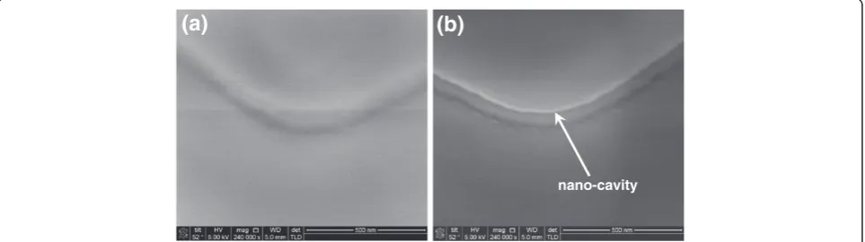
The key fabrication process flow of the proposed GAA JL NW FET is briefly described in Figure 1. First, a sand-wich stack of nitride/tetraethyl orthosilicate (TEOS) oxide/nitride layers was sequentially deposited and then patterned on a Si substrate capped with a 200-nm-thick wet oxide. Next, the formation of a sub-100-nm cavity
underneath both sides of the top nitride was fulfilled by selective lateral etching of the TEOS oxide layer using diluted hydrofluoric (HF) solution (HF:H2O = 1:100) as shown in Figure 1a. The scanning electron microscopic (SEM) images before and after cavity formation are depicted in Figure 2. With 60-s etching time, a vivid shape of cavity was formed and served as the template for the formation of NW channels. Anin situphosphorus-doped poly-Si layer was then deposited at 550°C using a mixture of SiH4/PH3gases in the LPCVD system (Figure 1b), fol-lowed by an anisotropic plasma etching to define the NW doped channels (denoted as DC) and S/D regions simul-taneously to form the structure without junctions (i.e., n+-n+-n+), as illustrated in Figure 1c. Note that the conventional control devices (i.e., n+-i-n+) were also processed along with a similar flow but using undoped poly-Si as the channel (denoted as undoped channel, UC), while the S/D regions were formed with the same
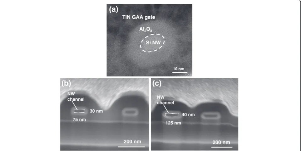
in situ doped poly-Si as in the DC device. To imple-ment the GAA structure, the sandwich stack layers were removed to suspend the NW channels, as revealed in Figure 3 with various volumes of NWs. Subsequently, the high-κ/metal gate stack structure was formed using the atomic-layer deposition system to conformally deposit 10-nm Al2O3 and 10-nm TiN films onto the NW channel, as shown in Figure 1d. Note that the final thickness of the TiN gate electrode is 150 nm by adding another 140-nm TiN film through sputtering. After patterning the gate electrode, deposit-ing passivation layer, and standard metallization proced-ure, the fabrication of NW devices was accomplished. Figure 4a shows the cross-sectional transmission electron microscopic (TEM) image of a GAA NW device with NW channel dimensions of about 11 × 15 nm. In this study, NW channels with the cross section of such dimensions for DC and UC devices are used for characterization un-less mentioned otherwise.
In this study, Hall measurements were conducted on a blanket in situ doped poly-Si thin film of 3,000 Å; the
SiO2
Substrate Si3N4 Doped poly-Si
Si3N4 SiO2
Substrate Si3N4
Buried oxide Buried oxide
Si3N4
Si3N4 SiO2
Substrate Si3N4
Buried oxide Poly-Si
NW
Substrate
Buried oxide Gate Al2O3
(a)
(b)
[image:2.595.57.290.91.252.2](c)
(d)
Figure 1Schematic process flow of the proposed GAA JL NW device.(a) A sandwich stack of nitride/TEOS oxide/nitride layers was sequentially deposited and then patterned on a Si substrate capped with a 200-nm-thick wet oxide. Next, selective lateral etching of the TEOS oxide layer was performed using diluted HF solution to form a sub-100-nm cavity underneath both sides of the top nitride. (b) Deposition of anin situphosphorus-doped poly-Si layer. (c) The NW doped channels (denoted as DC) and S/D regions were defined simultaneously. (d) After etching off the nitride and oxide surrounding the NW channels, the high-κ/metal gate stack structure was formed using the atomic-layer deposition system to conformally deposit 10-nm Al2O3and 10-nm TiN films onto the NW channel.
nano-cavity
[image:2.595.58.540.570.705.2](a)
(b)
carrier concentration of PH3with 15 sccm flow rate was found to be around 1 × 1020cm−3. However, the practical active carrier concentration in the NW channels of the
fabricated devices would be much lower than the result of Hall measurements due to the effects of film volume [10] and donor deactivation occurring in the Si NW structure [11].
1µµm Tiny NWs
Source
(a)
1µm
(b)
Mid-sized NWs
1µm
(c)
[image:3.595.57.537.88.365.2]Large-sized NWs
Figure 352° tilted SEM images of different sized NW devices before the gate stack formation.(a) A tiny NW device showing NWs exposed on both sides of the temporary dielectric step, (b) a mid-sized NW device, and(c)a large-sized NW device.
10 nm
Al2O3 TiN GAA gate
Si NW
(a)
200 nm 75 nm
30 nm NW
channel
(b)
200 nm 125 nm
40 nm NW
channel
(c)
Figure 4TEM and SEM images of a DC device.(a) Cross-sectional TEM image of a DC device with tiny NW covered with Al2O3/TiN GAA stack.
[image:3.595.60.539.453.693.2]Results and discussion
Transfer characteristics of the DC and UC NW FETs are depicted in Figure 5, in which another two DC NW devices with larger channel cross sections are also com-pared to illustrate the volume effect on the switching behaviors. The cross-sectional dimensions of the NWs for these two larger devices are 75 × 30 nm (mid-sized DC) and 125 × 40 nm (large-sized DC), respectively, as shown in Figure 4b,c. Apparently, more aggravated switching properties are observed for larger NW chan-nels among the three splits of DC devices. Owing to the conduction mechanism of the junctionless scheme, the bulk conduction path in the channel is not apt to be fully depleted as the channel cross section increases [7]. Therefore, for the mid-sized and large-sized DC devices,
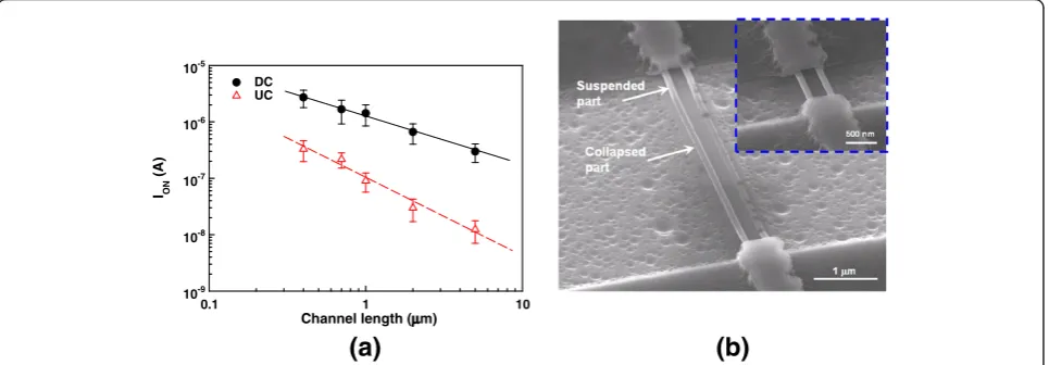
they cannot be effectively turned off by the gate, even though a high gate bias (VG) of −10 V is applied as revealed in Figure 5. On the other hand, the DC device with small NW channels displays superior switching behaviors with a subthreshold swing of 210 mV/dec and on/off current ratio of 7 × 10⁶, outperforming its UC counterpart with the current ratio of 2 × 10⁶. In the above comparison, the on current (ION) is defined as the drain current (ID) atVG−Vth= 2 V, while the off current (IOFF) is the minimalID. Figure 6a compares the on cur-rents, extracted at VG−Vth= 2 V and VD= 0.5 V from both types of devices, as a function of channel length (L). In our device structure, the channel length is defined as the spacing between the S/D regions. TheIONis evi-dently boosted in the DC devices, especially as the
L = 0.4 m VD = 0.5 V
V G (V)
-10 -8 -6 -4 -2 0 2 4 6
ID
(A)
10-14 10-13 10-12 10-11 10-10 10-9 10-8 10-7 10-6 10-5 10-4
[image:4.595.57.294.88.259.2]DC UC Mid-sized DC Large-sized DC
Figure 5Transfer characteristics of the DC and UC NW devices.
Mid-sized (75 × 30 nm) and large-sized (125 × 40 nm) DC NW devices are also plotted for comparison. All the devices characterized here are with channel length of 0.4μm.
10 1
0.1 ION
(A)
10-9 10-8 10-7 10-6 10-5
DC UC
(a)
(b)
Figure 6On currents and 52° tilted SEM image of a NW device.(a) On currents, extracted atVG−Vth= 2 V andVD= 0.5 V, as a function of
channel length for DC and UC devices. (b) 52° tilted SEM image of a NW device withL= 5μm showing collapse of NWs in the central channel region. The inset shows a NW device withL= 1μm depicting normal suspension of NWs between the S/D regions.
0 1 1
1 . 0 Vth
(V)
-2 0 2 4 6
[image:4.595.306.538.88.256.2]DC with Al2O3 UC with Al2O3 DC with SiO2
Figure 7Threshold voltage as a function of channel length for DC and UC devices.DC devices with GAA TiN/SiO2gate stack are
[image:4.595.58.541.526.694.2]channel length is long. This is attributed to the much larger cross section available for carrier flow, leading to the reduction in the channel resistance for the DC devices [7,8]. Besides, the carriers available for conduc-tion in the DC devices also outnumber those in the UC counterparts. Nevertheless, for shorter channels, the enhancement is not so pronounced. We ascribe this to two plausible reasons. For one, the series resistance in the S/D regions (RSD) for the DC devices is still high and could contribute to this trend as the channel length decreases, although RSD has been demonstrated to be reduced in the junctionless scheme as compared with its counterpart with junctions [8,12]. In order to further boost the ION enhancement, the S/D regions should be silicided or doped with higher concentration. Besides, as can be seen in Figure 6b, due to the small and long NW structure, the region of NW channel located away from the supporting source/drain ends tends to tumble down and might touch the substrate surface. However, for a shorter-channel device, the NWs normally suspend between the S/D regions as depicted in the inset. Thus, after the gate stack formation, the actual gate structure in the central part of a long channel may not be in a perfect gate-all-around configuration. Since the conduction mechanism in the DC and UC transistors is mainly through bulk and surface paths, respectively, the central region of the channel would be induced with fewer carriers for the UC device. As a result, theION enhance-ment for the DC transistors becomes larger as channel length increases, and this result may also imply that the DC device is less susceptible to gate configuration in the on-regime.
Figure 7 shows the threshold voltage as a function of channel length for both types of devices. The smallerVth values found in the DC devices are a result of the accumulation-mode operation. Due to the large work-function difference between the n+-doped NW channels and TiN gate, reasonable Vthvalues can be achieved for the DC devices. Furthermore, as compared with their counterparts with SiO2 gate dielectric, positive Vth values found in the DC devices with Al2O3 could be ascribed to the effect of negative fixed charges contained in Al2O3. Besides, no obvious Vth roll-off behaviors are observed in both types of devices with Al2O3, suggesting the effectiveness of the GAA structure and high-κ gate dielectric exploited.
Conclusions
In summary, we have reported the fabrication and ex-perimental investigation of the junction-free GAA NW device with TiN/Al2O3gate stack structure by employing an implant-free method. From the results of the elec-trical characterizations, a sufficiently small cross section of the NW channels is essential to obtain superior on/off
current ratio for heavily doped channel devices. The fabri-cated DC devices also show excellent Vthroll-off proper-ties and boosted on-state performance especially as the channel length increases. The adoption of Al2O3as the gate dielectric shifts theVthto a positive value and thus is conducive to acquiring desirable Vth. With its low cost and straightforward processing, we believe that the proposed GAA NW JL transistor architecture is promis-ing for future 3-D electronics and system-on-panel applications.
Competing interests
The authors declare that they have no competing interests.
Acknowledgment
The authors would like to thank the National Nano Device Laboratories (NDL) and Nano Facility Center (NFC) of National Chiao Tung University for assistance in device fabrication. This work was supported in part by the Ministry of Education in Taiwan under Aim for the Top University (ATU) Program and in part by the National Science Council of the Republic of China under contract No. 99-2221-E-009-167-MY3.
Author details
1Nano Facility Center, National Chiao Tung University, Hsinchu 300, Taiwan. 2Department of Electronics Engineering and Institute of Electronics, National
Chiao Tung University, Hsinchu 300, Taiwan.3Department of Electrophysics,
National Chiao Tung University, Hsinchu 300, Taiwan.4National Nano Device
Laboratories, Hsinchu 300, Taiwan.
Authors’contributions
CJ carried out the SEM and TEM characterization, performed the electrical analysis, and drafted the manuscript. TI fabricated the samples and carried out the electrical characterization. HC participated in the design and coordination of the study. All authors read and approved the final manuscript.
Received: 30 November 2011 Accepted: 22 June 2012 Published: 22 June 2012
References
1. Yeo KH, Suk SD, Li M, Yeoh YY, Cho KH, Hong KH, Yun S, Lee MS, Cho N, Lee K, Hwnag D, Park B, Kim DW, Park D, Ryu BI:Gate-all-around (GAA) twin silicon nanowire MOSFET (TSNWFET) with 15 nm length gate and 4 nm radius nanowires. InInternational Electron Devices Meeting: December 11–13 2006. San Francisco. Piscataway: IEEE; 2006:1–4.
2. Appenzeller J, Knoch J, Björk MT, Riel H, Schmid H, Riess W:Toward nanowire electronics.IEEE Trans Electron Devices2008,55:2827. 3. Suk SD, Li M, Yeoh YY, Yeo KH, Ha JK, Lim H, Park HW, Kim DW, Chung TY,
Oh KS, Lee WS:Characteristics of sub-5-nm trigate nanowire MOSFETs with single- and poly-Si channels in SOI structure. InVLSI Symposium Technology: June 16–18 2009; Honolulu. Piscataway: IEEE; 2009:142. 4. Singh N, Agarwal A, Bera LK, Liow TY, Yang R, Rustagi SC, Tung CH, Kumar
R, Lo GQ, Balasubramanian N, Kwong DL:High-performance fully depleted silicon nanowire (diameter≤5 nm) gate-all-around CMOS devices.IEEE Electron Device Lett2006,27:383.
5. Im M, Han JW, Lee H, Yu LE, Kim S, Kim CH, Jeon SC, Kim KH, Lee GS, Oh JS, Park YC, Lee HM, Choi YK:Multiple-gate CMOS thin-film transistor with polysilicon nanowire.IEEE Electron Device Lett2008,29:102.
6. Hsu HH, Lin HC, Luo CW, Su CJ, Huang TY:Impacts of multiple-gated configuration on the characteristics of poly-Si nanowire SONOS devices.
IEEE Trans. Electron Devices2011,58:641.
7. Colinge JP, Lee CW, Afzalian A, Akhavan ND, Yan R, Ferain I, Razavi P, O’Neill B, Blake A, White M, Kelleher AM, McCarthy B, Murphy R:Nanowire transistors without junctions.Nature Nanotechnol2010,5:225. 8. Su CJ, Tsai TI, Liou YL, Lin ZM, Lin HC, Chao TS:Gate-all-around
9. Wilk GD, Wallace RM, Anthony JM:High-κgate dielectrics: current status and materials properties considerations.J Appl Phys2001,89:5243. 10. Lacy F:Developing a theoretical relationship between electrical
resistivity, temperature, and film thickness for conductors.Nanoscale Research Lett2011,6:636.
11. Björk MT, Schmid H, Knoch J, Riel H, Riess W:Donor deactivation in silicon nanostructures.Nature Nanotechnol2009,4:103.
12. Lee CW, Lederer D, Afzalian A, Yan R, Dehdashti N, Xiong W, Colinge JP:
Comparison of contact resistance between accumulation-mode and inversion-mode multigate FETs.Solid State Electron1815,2008:52.
doi:10.1186/1556-276X-7-339
Cite this article as:Suet al.:Low-temperature poly-Si nanowire junctionless devices with gate-all-around TiN/Al2O3stack structure
using an implant-free technique.Nanoscale Research Letters20127:339.
Submit your manuscript to a
journal and benefi t from:
7Convenient online submission 7Rigorous peer review
7Immediate publication on acceptance 7Open access: articles freely available online 7High visibility within the fi eld
7Retaining the copyright to your article