Technology (IJRASET)
Design and implementation of transmission of
128-bit digital data generated from a data generation
unit from one base station to another base station
with its reception at the receiver end using
“Hamming (224,128) Code technique” written in
VHDL code
Paresh Kumar Pasayat1, Sonam Barik2 1
Assistant Professor, Dept. of ETC Engg., I.G.I.T. Government Engineering College, India
2
M.Tech. Student [ETC], Dept. of ETC Engg., I.G.I.T. Government Engineering College,India
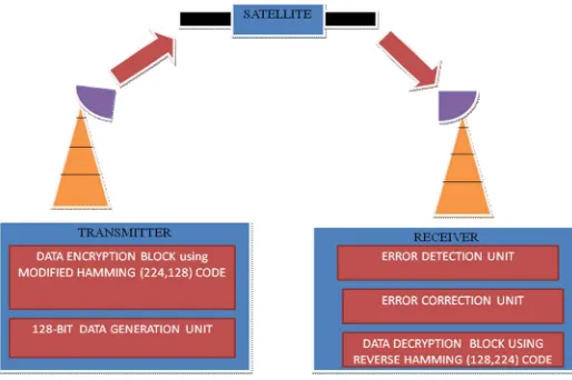
Abstract- The proposed paper mainly deals with the generation of the 128-bit digital data using a data generation unit with it transmission and reception over space. The data generation unit consists of control unit, data path unit, memory unit and back-up unit. The desired 128-bit data is encrypted before transmission using Hamming (224,128) code technique to produce 224-bit encrypted data. The encrypted data is received at the receiver end and passed through the error detection unit and the error is corrected if it is present in the data. Then, the corrected 224-bit encrypted data is decrypted using reverse Hamming (128,224) code technique. The main advantage of using Hamming code technique is that it provides both error detection and correction in the encrypted data. The proposed work can best be implemented in providing high security to the digital data. This can be used in the banking sector, military sector, telecommunication sector. The proposed work is done by using VHDL language. The code is tested and simulated using Xilinx ISE9.2i software.
Index Terms: ALU (Arithmetic Logic Unit), Encryption, Decryption, VHDL (Very High speed Integrated Circuit Hardware Description Language).
I. INTRODUCTION
Technology (IJRASET)
[image:3.612.176.433.108.279.2]II. PROJECTMODEL
Fig. 1: Project model of the proposed project
III. LOGICUSEDINTHEPROPOSEDDESIGN
A. Data generation unit
The data generation unit is used to generate the desired 128-bit digital data that are sent during transmission. The data generation unit is composed of several units like data path unit, control unit, memory unit and backup unit.
1) Control unit: It is needed to generate the control signals automatically at every cycle. It is a finite state machine. By stepping through a sequence of states, the control unit controls the operations of the data-path. For each state the output logic that is inside the control unit will generate all of the appropriate control signals for the data-path to perform different arithmetic and logic operations.
2) Datapath unit: This is a collection of functional unit such as arithmetic logic unit (ALU) that performs data processing operation. The ALU is a building block of the data generation unit that performs many operations based on the control inputs. The ALU can perform basic arithmetic functions such as addition, subtraction etc and logic functions including logic AND, logic OR, and logic XOR etc. The various functions and the corresponding functional units are:-
3) Memory unit: It is used as storage purpose of the data generation unit. The information to be stored is of two types, data information and program information. Memories are used for storage of both instructions and data. The process of storing data into memory is called writing and retrieving data or op-code from the memory is called reading. The memory unit works only when the chip enable signal is at high level.
4) Backup unit: It is used to store the final output of the data-path unit. It is the replica of the memory unit which helps to store the output in case memory unit fails. It also helps the data generation unit to work with less burden.
B. Algorithm For Encoding Unit
Step 1
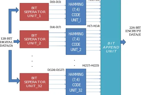
First, 128-bit data is divided into 32 nos. of words each consisting of 4-bit data. Step 2
The 7-bit Hamming (7,4) code encoding technique is applied to each word. For each word, the encoding unit generates 7-bit encoded data. The logic for implementing the Hamming code technique is given as follows:
Suppose, the 4-bit data (B) to be encoded is B3B2B1B0 and the 7-bit Hamming code (H) generated is H6H5H4H3H2H1H0. Here, the value for each bit of H is given as follows:
Technology (IJRASET)
H2 = B2 H1 = B1 H0 = B0
Step 3
After that the Hamming codes corresponding to each word are appended to form the desired 224-bit encoded data.
C. Algorithm For Error Detection And Correction Unit Step 1
To decode a Hamming code, checking needs to be done. The decoding has been done in word-by-word basic. Let us take A2A1A0 be a parity word consisting of three bits which is used to detect the error in the received data. The values of A are given as follows: A0 = H0 xor H2 xor H4 xor H6
A1 = H6 xor H5 xor H2 xor H1 A2 = H6 xor H5 xor H4 xor H3
Step 2
If the value of A2A1A0 is equal to “000”, then there is no error in the received data and the data can be decoded to get the exact replica of the transmitted data.
Step 3
If the value of A2A1A0 is not equal to “000”, then there is error in the received data and the checking is done in which bit, the error is present. For example, A2A1A0 = “001”, then the first bit of H from MSB is having error.
Step 4
In order to correct the error, the bit of H in which the error is present has to be complemented (i.e. ‘0’ is replaced by ‘1’ and ‘1’ is replaced by ‘0’). After correcting the error, the corrected encoded data can be decoded by using decryption algorithm.
[image:4.612.184.422.413.574.2]HAMMING (7,4) CODE UNIT_2 HAMMING (7,4) CODE UNIT_32 128-BIT DIGITAL DATA(D) BIT SEPERA TOR UNIT_1 HAMMING (7,4) CODE UNIT_1 BIT SEPERA TOR UNIT_2 BIT SEPERA TOR UN IT_32 BIT APPEND UNIT 224-BIT ENCRYPTED DATA(E) D(0)-D(3) D(4)-D(7) D(124)-D(127) H(0)-H(6) H(7)-H(14) H(217)-H(223) . . . . .
Fig. 2: Block diagram showing the 128-bit encryption
D. Algorithm for Receiver Unit Step 1
In order to decode the 224-bit corrected encoded data, the data is divided into 32 nos. of blocks each generating 7-bit encoded data. Step 2
Then, the following logic has been used to obtain the original 128-bit data transmitted at the transmitter end after appending all 4-bit data generated from 32 nos. blocks used for decoding unit in the receiver circuit. Let us take, the 7-bit corrected encoded data is C & the 4-bit data generated from the decoding unit is R.
Technology (IJRASET)
R=R(3) & R(2) & R(1) & R(0)
R(0) = C (0)
R(1) = C (1) R(2) = C (2)
R(3) = C (4)
Step 3
The step has been repeated for all the 32 nos. of blocks each consisting of 7-bit corrected encoded data input. All the 4-bit output datas (R) are appended to produce 128-bit decoded data which is the exact replica of the 128-bit data transmitted at the transmitter end.
BIT SEPERA TO R
UN IT_1
BIT SEPERA TO R
UN IT_1
PARITY WORD WITH CORRECTED ENCRYPTED DATA
GENERATION UNIT_2
PARITY WORD WITH CORRECTED ENCRYPTED DATA GENERATION UNIT_32 224-BIT ENCRYPTED DATA(E) BIT SEPERA TO R
UNIT_1
[image:5.612.182.431.201.386.2]PARITY WORD WITH CORRECTED ENCRYPTED DATA GENERATION UNIT_1 DECRYPT ION UNIT UNIT 128-BIT DECRYPTED DATA(I) H(0)-H(6) H(7)-H(14) H(217)-H(223) . . . . . DECRYPT ION UNIT UNIT DECRYPT ION UNIT UNIT B IT A P P EN D U N IT A(0)-A(2) A(3)-A(6) A(93)-A(95) C(0-6) C(7-13) C(218-223)
Fig. 3: Block diagram showing the 128-bit decryption
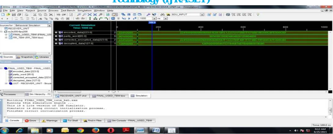
IV.RESULTANDDISCUSSION
[image:5.612.43.572.444.705.2]Technology (IJRASET)
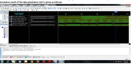
Fig. 5: Simulation result of 128-bit data generation unit with chip_enable=’0’.
[image:6.612.42.588.414.716.2]Technology (IJRASET)
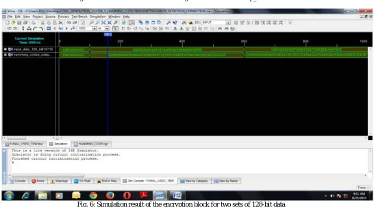
Fig. 7: Simulation result of the decryption block with 224-bit as the encrypted data corresponding to the 1st input data
V.ADVANTAGES
The proposed work is having various advantages such as providing data and network securities, less combinational path delay due to the better placement of modules, simultaneous transmission of higher bit data (i.e. 128-bit) etc. Another advantage is the used of back-up unit which works only when the memory unit of the data generation unit fails to give the desired output.
VI.APPLICATIONS
The proposed design can be used in the field of banking sector, military sector, telecommunication industry and any other sectors which are used to communicate with the people within the organization using data security techniques (intranet & internet).
VII.CONCLUSION
At the end of the proposed work, the 128-bit data generation unit and data security unit has been successfully designed with error detection and correction of 128-bit digital data at the receiver end using VHDL code and the desired results have been obtained. The proposed design of data security unit is having less combinational path delay resulting faster operation and less power consumption as compared to other data security algorithms except substitution cipher and transposition cipher.
REFERENCES
[1] Marri Mounika, Aleti Shankar, “Design & Implementation Of 32-Bit Risc (MIPS) Processor”, International Journal of Engineering Trends and Technology
(IJETT) – Volume 4 Issue 10 - Oct 2013.
[2] Rekha Halkatti,Veeresh Pujari,“FPGA based 128-bit customised vliw processor for executing dual scalar/vector instructions”, Volume: 03 Special Issue: 03 | May-2014 | NCRIET-2014,eISSN: 2319-1163 | pISSN: 2321-7308.
[3] Balpande, R.S. and Keote, R.S., “Design of FPGA based Instruction Fetch & Decode Module of 32-bit RISC (MIPS) Processor”, in Proc. of International Conference on Communication Systems and Network Technologies, pp. 409-413, 2011.
[4] Manoranjan Pradhan, “Simulation and Verification of Self Test 16-Bit Processor”, International Journal of Computer Applications (0975 – 8887) Volume 20–
No.1, pp.42-45,April 2011.
[5] Nupur Gupta, Progoti Gupta, Himansi Bajpai, Richa Singh,Shilpa Saxena, “Analysis of 16 bit Microprocessor Architecture on FPGA using VHDL” International
journal Of Advanced Research in Electrical, Electronics and Instrumentation Engineering, Volume 3, Issue 4,April 2014.
[6] W.Stallings,“Cryptography and Network Security”, 2nd Edition, Prentice Hall.
[7] Christof Paar, Jan Pelzl, “The Data Encryption Standard (DES) and Alternatives”, “Understanding Cryptography”, Springer.
[8] Bruce Schneir: “Applied Cryptography”, 2nd edition, John Wiley & Sons.
[9] A.Litwin,“Cryptography and Network Security” LOS Alamitos,CA:IEEE computer society press.
[10] Douglas L. Perry. “VHDL Programming by Examples”, TMH.
[11] Hamacher, Vranesic, and Zaky. “Computer Organization”, 5th edition, New York: McGraw-Hill Companies.
Technology (IJRASET)
[14] Rajdeep Chakarborty, Dr. J.K Mandal , “ A Microprocessor-Based Block cipher through Rotational Addition Technique ”, IEEE 9thinternational conference on
information and technology,2006.
[15] Ke Wang ,“ An encrypt and decrypt algorithm implimentation on FPGAS”, IEEE, Department of information engineering, 2009.
[16] H. Lee Kwang , “ Basic Encryption and Decryption” , Computer and Electrical , 1967.
[17] Ranjan Bose,“Information Theory, Coding and Cryptography” , chapter -8.
[18] W.Diffie; M.E.Hell man, “ New Directions in Cryptography” IEEE transaction theory, Nov, pp 644-654.
[19] Geetanjali and Nishant Tripathi, “VHDL Implementation of 32-bits arithmatic logic unit(ALU)” International Journal of Engineering Trends and Technology
(IJETT),Emerging trends in Engineering ICETIE-2012.
[20] Anushka Pakrashi,“Design and implementation of 32-bits ALU on XILINX FPGA Using VHDL”.
[21] Dr. Malti Bausal , “Implentation of 32-bits arithmatic logic unit on xilinx using VHDL.” Department of electronics and communication Engineering.
[22] Shikha Khurana,Kanika Kaur , “Implentation of ALU using FPGA”, International Journal of Engineering Trends and Technology ,2002.
[23] David A. Patterson and John L. Hennessy “Processor implentation in VHDL”, computer organisation and design,06-07-2007.
[24] Alpesh kumar Dauda ,Nalinikanta Barpanda ,Nilamani Bhoi, “ Control Unit Design of a 16_Bit processor using Vhdl” , International journal Of Advanced
Research in Electrical, Electronics and Instrumentation Engineering, Dec-2013.
[25] Jen- Shiun Chiany and Jun-Yao Liao , “ A novel asynchoronous control unit and Application to a pipelined multiplier” , IEEE pp.11169-172 1998.
[26] Xiao Tiejun, Lia Fang , “ 16_bits Teaching microprocessor design and application”, IEEE international symporium of IT in Medicine and Education ,pp
160-163,2008.
[27] Kui YI ,Yue-Hua Ding , “ 32_bit RISC CPU based on MIPS instructation fetch Module Design” , International joint conference on Artificial intelligence, pp
754-760,2009.
[28] Ronald J. Hayne, American society for engineering education ,“An Instructional Processor Design using VHDL and FPGA”, AC-2011.