© 2017, IRJET | Impact Factor value: 5.181 | ISO 9001:2008 Certified Journal | Page 3351
DSP Based Voltage Controlled Single Stage PFC Converter with
Synchronous Rectification
Litty Joseph
1, Neetha John
2, Sija Gopinathan
31
PG Student[PE], Dept. of Electrical and Electronics Engineering, Mar Athanasius College of Engineering
Kothamangalam, Kerala, India
2,3
Assistant Professor, Dept. of Electrical and Electronics Engineering, Mar Athanasius College of Engineering
Kothamangalam, Kerala, India
---***---Abstract -
Synchronous switching power converters give
better performance than non-synchronous converters in low output voltage, high output current systems applications. This work presents a single stage PFC synchronous rectifier, which
has low switch voltage stress with high efficiency
implementing a constant output voltage and bus voltage. A single stage isolated AC/DC PFC converter with synchronous rectification for high DC-link voltage low-power applications, achieved through an effective integration of AC/DC and DC/DC stages, where all of the switches are shared between two operations. With the converter and switching scheme, input current shaping and output voltage regulation can be achieved simultaneously without introducing additional switches or switching actions. Due to the flexible DC-link voltage structure, high power factor can be achieved at high line voltage. Proposed system provide high power factor with controlled output and bus voltage. The performance of the single stage PFC converter is simulated in the MATLAB/SIMULINK environment. C2000 Piccolo Launchpad DSP processor is used to generate the control pulses and setup a prototype model of voltage controlled single stage PFC with synchronous rectification.
Key Words
:
DC-link voltage, Single stage PFC converter,
Synchronous rectification, Zero voltage switching, High
power factor
1. INTRODUCTION
AC/DC power converters are required to operate with high power factor (PF) and low total harmonic distortion (THD) for improved grid quality and full capacity utilization of the transmission lines. Passive PF correction (PFC) circuits consist of inductive and capacitive filters followed by a diode bridge provide the simplest way of achieving high PF with high efficiency; however, they require low line frequency filters which are bulky and heavy. In order to operate at high frequency and reduce the size of the circuit, high frequency two-stage active PFC converters have been used [1]. In this architecture, a front-end AC/DC PFC converter is operated with a switching frequency in the order of tenths to several hundred kHz for converters with Si semiconductor devices, and from several hundreds of kHz to tenths of MHz with wide band gap devices, to shape the input current close to sinusoidal waveform in phase with the grid voltage . The
second stage DC/DC converter provides the galvanic isolation and output voltage regulation. The controllers of the two stages are completely independent. The flexibility in control allows optimizing power stages, fast output voltage regulation and operating with high PF and low THD. However, this method comes with the expense of more components and larger size. Moreover, the constant switching losses such as parasitic capacitance losses associated with power switches reduce the efficiency of the converter at light load condition. This study proposes a new SSTL isolated AC/DC PFC converter for high DC link voltage and low power applications, achieved with complete integration of two stages, where all of the switches are shared between input current shaping and output voltage regulation stage[1]. In comparison with the existing three level single stage topologies, the converter offers minimum number of components as of three level AC/DC converter, and does not require any auxiliary circuit other than a diode bridge and an inductor. The topology can serve as a low cost power electronic interface intended for applications requiring high-voltage DC link. Two independent control algorithms, embedded in a single microcontroller, are used to achieve PFC and output voltage regulation[1]-[4] .This feature allows having lower output current ripple and less distorted input current even at light load condition. In addition switches are turned on under zero voltage, which increases the efficiency of the converter in comparison to hard-switched AC/DC single stage converter. Furthermore, higher PF can be achieved at high line voltage due to the flexible DC link voltage structure. But the system has more power loss thus it has less efficiency. In order to increase efficiency synchronous rectification method is used [8]. Synchronous Rectification (SR) the use of MOSFETs to achieve the rectification function typically performed by diodes. SR improves efficiency, thermal performance, power density, manufacturability, and reliability, and decreases the overall system cost of power supply systems .
2.
SINGLE STAGE PFC SYNCHRONOUS RECTIFIER
© 2017, IRJET | Impact Factor value: 5.181 | ISO 9001:2008 Certified Journal | Page 3352
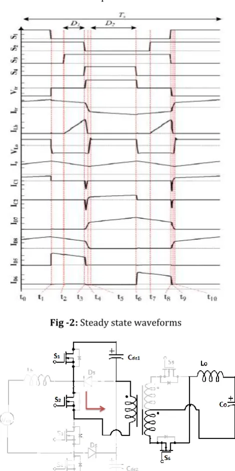
Fig -1: Single stage PFC synchronous rectifierHere, the inductor is charged when S2 and S3 are turned on
simultaneously. Body diodes of S1 and S4 serve as the boost
diode of the PFC boost converter. At the same time, S1 to S4
are switched to apply Vdc/2,-Vdc/2, and zero voltage across
the primary side of the transformer. Thus, all of the switches are shared between the two stages, which makes it fully integrated single-stage converter without any additional auxiliary switches. When a boost inductor and a diode bridge is added to the nodes the overlap of gate signals of S2 and S3
enables applying input voltage across the boost inductor[1]. The steady state wave form of the converter is given in fig.2. The switches S2-S3 and S1-S4 have 180 degree phase shift
with respect to each other. The duty ratios of S2-S3 should be
greater than 0.5 such that two signals overlap. Here, the circuit is explained considering that input inductor current is discontinuous and the switching scheme is as follows; S1 is
turned on right after S3 is turned OFF, and similarly, S4 is
turned on when S2 is turned OFF. A dead-time should be
inserted in between the turning ON instant of S1 and turning
OFF instant of S3 and likewise between switching of S2 and S4
to avoid short-circuit. Synchronous switching power converters give better performance than non synchronous converters in low output voltage, high output current systems applications. Synchronous Rectification (SR) the use of MOSFETs to achieve the rectification function typically performed by diodes. Proposed system provide high power factor with controlled output and bus voltage. The conduction loss of diode rectifier contributes significantly to the overall power loss in a power supply, especially in low output voltage applications. Schottky diodes were an improvement over the standard diode because their forward voltage is lower. But Schottky diodes also start from a fixed forward voltage. Higher efficiencies can be achieved by synchronously switching MOSFET devices to emulate diodes, taking advantage of the FET's low conduction losses.
3. OPERATING MODES
3.1. Mode 1
In this mode, both S2 and S2 are on. The upper capacitor, Cdc1,
discharges to the load by applying -Vdc/2 to the primary side
of the transformer. The primary side current increases linearly under constant voltage. S5 turn ON at the secondary
side of the transformer. In this mode, the boost inductor, Lb
[image:2.595.318.553.121.591.2]does not interfere to the operation of the circuit.
Fig -2: Steady state waveforms
Fig -3: Equivalent circuit of mode 1
3.2. Mode 2
At t = t1, S1 is turned OFF and S2 is kept on. The current in
the leakage inductance conducts D5 and the primary side
current freewheels; hence, zero voltage is applied across the primary side of the transformer. The output inductor voltage is equal to -V0. The output inductor current decreases
© 2017, IRJET | Impact Factor value: 5.181 | ISO 9001:2008 Certified Journal | Page 3353
Fig -4: Equivalent circuit of mode 23.3. Mode 3
At t = t2, S3 is turned on, while S2 still remains on. The
primary current continues to freewheel and zero voltage is applied across the primary side; hence, the output inductor current continues to decrease under output voltage. Meantime, Vin is applied across Lb and input current
[image:3.595.305.555.101.226.2]increases linearly storing energy in the inductor.
Fig -5: Equivalent circuit of mode 3
3.4. Mode 4
In the beginning of this mode, S2 is turned OFF, S4 is turned
ON, while S3 is kept on. Within this time interval, the
following two operations are completed. The energy stored in the input inductor is transferred to the DC-link capacitors. The inductor current decreases linearly under Vin- Vdc.
Meantime, Vdc/2 is applied across the primary side of the
transformer. The current in the leakage inductance is transferred to Cdc2. This causes the output current to turn
OFF from S5 to S6 . At the end of this time interval, the energy
in the input inductor is completely transferred to the DC link capacitors and turning OFF of the switches S5 and S6 is
completed. Depending on the DC bus voltage, and input current, one of these operations ends earlier than the other one. In this case, the energy stored in Lb is transferred to the
DC link at t = t5.
Fig -6: Equivalent circuit of mode 4
3.5. Mode 5
Cdc2 discharges over to the load and Vdc/2 is applied across
the primary side of the transformer. The voltage across the output inductor is VL0 = (Vdc/2N) - V0. The input current
[image:3.595.312.567.352.479.2]remains at zero in DCM mode.
Fig -7: Equivalent circuit of mode 5
3.6. Mode 6
At t = t6, S4 is turned OFF, and only S3 is on. This allows
leakage current to freewheel through D6, and zero voltage is
[image:3.595.47.278.384.510.2]applied to the primary side. The output current decreases linearly under -V0.
[image:3.595.331.534.599.726.2]© 2017, IRJET | Impact Factor value: 5.181 | ISO 9001:2008 Certified Journal | Page 3354
3.7. Mode 7
At t = t7, S2 is turned ON. The energy from the input is stored
[image:4.595.340.528.154.290.2]in the inductor. This is similar to mode 3, except that this time the primary side current is opposite to that in mode 3 and freewheels through D6.
Fig -9: Equivalent circuit of mode 7
3.8. Mode 8
At the beginning of this interval, S3 is turned OFF, S1 is
turned ON, and S2 remains ON. This mode is similar to mode
4, where the stored energy in the inductor is transferred to the DC bus capacitors, and -Vdc/2 is applied to the primary
windings.
Fig -10: Equivalent circuit of mode 8
4. RESULTS AND DISCUSSION
4.1. Simulation Models and Results
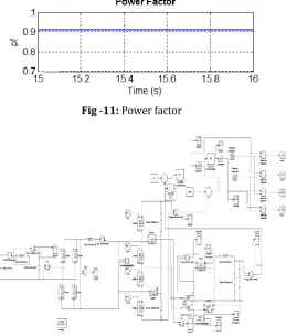
The simulation and experimental results are shown in this section. The proposed PFC synchronous rectifier is simulated in MATLAB. The simulink model of single stage PFC synchronous rectifier is shown in fig.12. Table 1 shows the specification of different parameters used. MOSFET is used as the switch. Switching pulses are applied to the MOSFET, interleaved at 180 degree phase shift. A repeating sequence of required frequency is compared with constants 0.6 and 0.4, the duty ratio to generate pulses with 60% ON and 40% ON time. Whenever repeating sequence is less than the constant, it will output a high value and if constant is smaller, it will output a low value. The converter exhibits high PF
[image:4.595.59.265.180.281.2]0.9173 with less number of switches/diodes. The single stagePFC converter has an output voltage of 49 V and DC-link voltage of 625 V. In order to get constant output voltage
Table -1: Simulation parameters
[image:4.595.55.270.414.520.2]and bus voltage at all load conditions introducing closed loop control for outputvoltage and bus voltage. For closed loop control of output voltage, output voltage is compared with a constant voltage 48(Reference voltage) and the error signal is given to a PI controller and the tuned signal from PI controller is used as new constant for pulse generation. Similarly for closed loop control of bus voltage, bus voltage is compared with a constant voltage 600(Reference voltage) and the error signal is given to a PI controller and the tuned signal from PI controller is used as new constant for pulse generation.
[image:4.595.314.574.435.740.2]Fig -11: Power factor
© 2017, IRJET | Impact Factor value: 5.181 | ISO 9001:2008 Certified Journal | Page 3355
Fig. 13 shows the switching pulses for the PFC converter.Fig -13: Switching pulses
The single stage PFC synchronous rectifier has less power losses compared to single stage PFC converter, which improves the efficiency of the system. Fig.14 shows power loss (7.5 W) and output voltage (10 V) of the system when diode is used instead of switch S5 and S6.
[image:5.595.40.296.320.408.2]Fig -14: Output voltage and power loss
Fig. 15 shows power loss (0.25 W) and output voltage (10 V) of the system when switch is used. SR improves efficiency, thermal performance, power density, manufacturability, and reliability, and decreases the overall cost of power supply systems
.
Fig -15: Output voltage and power loss
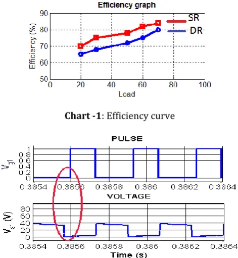
Efficiency curve for single stage PFC converter and PFC synchronous rectifier is plotted by varying load. Single stage PFC converter has an efficiency of 80% and PFC synchronous rectifier has 85%.
Chart -1: Efficiency curve
Fig -16: Zero voltage switching of switch 1
Soft switching of switches reduce the switching losses and increase efficiency. The switch S1 is turn on at zero voltage
(ZVS) as shown in fig.16
4.1. Experimental Setup and Results
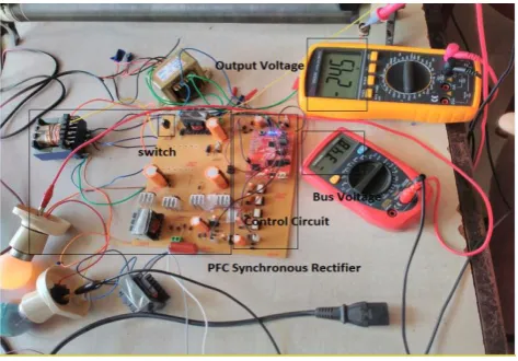
[image:5.595.47.280.525.608.2]Hardware setup is done in a Printed Circuit Board(PCB). Control circuit and power circuit are implemented in one PCB. A DSP controller TMS320C2000 which provides a high level of computational performance and programming flexibility is used as control circuit. Prototype is designed for an input voltage of 230 V, output voltage 24 V and bus voltage 300 V.
Fig -17: Control strategy
[image:5.595.313.580.554.650.2]© 2017, IRJET | Impact Factor value: 5.181 | ISO 9001:2008 Certified Journal | Page 3356
Output voltage is controlled to 24 V and DC-link voltage is [image:6.595.44.281.203.368.2]controlled to 350 V. Fig. 18 shows the experimental setup for voltage controlled single stage PFC Synchronous Rectifier 180 degree phase shifted pulse output from the controller TMS320C2000 is shown in fig.19 and output pulse from driver IC which is of 12 V. Both voltage across switch and pulse of switch 1 is shown in fig. 20, in order to verify the ZVS operation.
Fig -18: Experimental setup
180 degree phase shifted pulse output from the controller TMS320C2000 is shown in below and output pulse from driver IC which is of 12 V. The 12 V output is given to the gate of the switch.
Fig -19: PWM output
Soft switching of switches reduce the switching losses and increase efficiency. The switch S1 is turn on at zero voltage
(ZVS). Thus efficiency can be increased.
Fig -20: Zero voltage switching of switch 1
5. CONCLUSIONS
In this work a prototype model of voltage controlled single stage PFC with synchronous rectification is implemented. Synchronous switching power converters give better performance than non-synchronous converters in low output voltage, high output current systems applications. Single stage PFC synchronous rectifier, has been designed with low power loss, high efficiency, constant output voltage and bus voltage. Output voltage is controlled to 24 V and DC-link voltage is controlled to 350 V. The performance of the single stage PFC converter is simulated in the MATLAB/SIMULINK environment. C2000 Piccolo Launchpad DSP processor is used to generate the control pulses. PFC synchronous rectifier has high efficiency of 85% and get better power factor near to unity.
REFERENCES
[1] Serkan Dusmez, “A fully integrated three-level isolate single-stage PFC converter", IEEE Transactions on Power Electronics, vol. 30, no. 4, pp. 2050- 2062, April 2015
[2] J. R. Morrison and M. G. Egan, “A new modulation strategy for a buck boost input AC/DC converter", IEEE Transactions on Power Electronics, vol.29 [3] Hao Ma, “Design and analysis of single stage power
factor correction converter with a feedback winding", IEEE Transactions on Power Electronics, vol.25, no. 6, pp. 1460-1470, 2010.
[4] Y.W. Cho, J.M. Kwon, and B.H. Kwon, “Single power conversion AC/DC converter with high power factor and high efficiency", IEEE Transactions on Power Electronics, pp. 4797-4806, 2014.
[5] D. D. C. Lu, H.H.C.Iu, and V. Pjevalica, “A single stage AC/DC converter with high power factor, regulated bus voltage and output voltage", IEEE Transactions on Power Electronics, pp. 218-228, Jan. 2008. [6] H. Athab and D. Lu, “A single switch AC/DC flyback
converter using a CCM/DCM quasi active power factor correction front end", IEEE Transactions on Power Electronics, vol.59, no. 3, pp. 1517-1526, 2012.
[7] J. F. Chen, R. Y. Chen, and T. J. Liang, “Study and implementation of a single stage current fed boost PFC converter with ZCS for high voltage applications" IEEE Transactions on Power Electronics, vol. 23, no. 1, pp. 379-386, 2008. [8] Sung-Pei Yang and Jong-Lick Lin, “A novel ZCZVT
forward converter with synchronous rectification", IEEE Transactions on Power Electronics, vol. 21, no. 4, pp. 79-86, 2006.