© 2017, IRJET | Impact Factor value: 5.181 | ISO 9001:2008 Certified Journal | Page 1586
Design of Hardware Efficient High Efficiency Video Coding DCT
Surya G
1, Prof. Premanand B
21
M-Tech, Dept. of ECE, Government Engineering College, Idukki, Kerala, India
2Assistant Professor, Dept. of ECE, Government Engineering College, Idukki, Kerala, India
---***---Abstract -
The advent of digital videos having Ultra High Definition (UHD) resolution demands a proper way to conveniently transmit massive amount of High Definition (HD) content. Hence the video is compressed to reduce the quantity of data being transmitted. Transform operations like Discrete Cosine Transform (DCT) or Discrete Sine Transform (DST) are used in High Efficiency Video Coding (HEVC) encoders. As the DCT operations have high computational complexity, this work mainly focuses to develop a two dimensional (2D) HEVC DCT to reduce the hardware complexity and delay of the system. DCT architecture involving shifters and adders are replaced using Scalable Approximation DCT architecture which reduced the computational complexity, as the proposed system consists of only adders. The proposed system obtained a hardware efficiency of 12.93% and delay is reduced by 4.73%. HEVC 2D DCT hardware is designed using Verilog HDL and the hardware simulation is done in Xilinx Spartan 3E FPGA using Xilinx 14.2 ISE Design Suite.Key Words: High Efficiency Video Coding (HEVC),
Discrete Cosine Transform (DCT), Field Programmable Gate Array (FPGA), High Definition (HD), DCT approximation.
1. INTRODUCTION
Due to the advancement of technology in the multimedia applications, compression technique plays a vital role. There is a need to conveniently transmit large quantity of High definition (HD) content and hence several compression techniques are used to reduce the amount of transmitted data. A new international compression standard known as High Efficiency Video Coding (HEVC) was developed which is a potential successor to the broadly used H.264 standard [2]. It was developed by Joint collaborative team on video coding (JCT-VC). HEVC has 50% better video compression efficiency than H.264 standard. The transformation operation like Discrete Cosine Transform (DCT) plays a pivotal role in video compression [3]. The other main advantages of HEVC compared to H.264 standard are flexible block structure, larger encoding blocks and better approximations of DCT. Although HEVC has numerous advantages, the increase in computational complexity is its major constraint. DCT operations account for almost quarter of the computational complexity of HEVC encoder. Hence many research works are done in order to reduce the complexity of the hardware. The main focus of this work is to obtain a hardware efficient HEVC DCT, so as to reduce the computational complexity. HEVC is widely used in many applications like broadcast of
High Definition (HD) TV signals over satellite, cable and terrestrial transmission systems. HEVC finds application also in video content acquisition and editing systems, camcorders, security applications, mobile network video and real-time conversational applications such as video chat and video conferencing.
2. HEVC 2D DCT HARDWARE
As HEVC DCT has high computational complexity, a computation reduction technique is required. HEVC 2D DCT hardware [1] is shown in Fig 1.
Fig -1: HEVC 2D DCT Hardware [1]
Inorder to select the proper DCT inputs for each TU size, input splitters are used and output multiplexers are used to select the proper DCT outputs. Since HEVC DCT algorithm allows performing an N-point 1D DCT by performing two N/2-point 1D DCTs with some preprocessing, the hardware performs N-point 1D DCT transforms by performing two N/2-point 1D DCT transforms with an efficient butterfly structure. It performs 2D DCT by initially performing 1D column DCT transform of a TU, and then performing 1D DCT transform on the rows of the TU. After 1D column DCT, transpose memory is used to store the resultant coefficients and these coefficients are used as input for 1D row DCT.
[image:1.595.311.557.344.500.2]© 2017, IRJET | Impact Factor value: 5.181 | ISO 9001:2008 Certified Journal | Page 1587 datapaths and one 8x8 datapath are used for 16x16 TU size.
All datapaths (two 4x4, one 8x8 and one 16x16) are used for 32x32 TU size. DCT multiplications are performed in the datapaths using only adders and shifters in the existing system. In the proposed system, scalable approximation DCT is used which consists of only adders.
Fig -2: Column butterfly structure [1]
3. HEVC 2D DCT HARDWARE USING DCT
ARCHITECTURE INVOLVING SHIFTERS AND
ADDERS
Fig -3: Block Diagram of Existing System
3.1 Input Splitter
Input splitter is used to select the proper DCT inputs for each TU size.
3.2 32 Point DCT Structure Using Shifters and
Adders
DCT is generally used in data compression applications internationally due to good de-correlation properties. Several integer DCT structures have been suggested from the last two decades inorder to reduce the complexity of DCT computations [4],[5].
3.2.1 Architectures for Integer DCT Computation
i) Architecture for Four-Point Integer DCT
The four-point integer DCT architecture [6] is shown in Fig. 4. It is composed of an input adder unit (IAU), a shift-add unit (SAU), and an output adder unit (OAU). The IAU computes a(0), a(1), b(0), and b(1) according to STAGE- 1 of
the algorithm as described in Table 5.1. ti,36 and ti,83 are
computed by two SAUs according to STAGE-2 of the algorithm. t0,64 and t1,64 can be computed without consuming
any logic since the shift operations could be rewired in hardware. The structure of SAU is shown in Fig. 4 (b). Outputs of the SAU are finally added by the OAU according to STAGE-3 of the algorithm.
Fig -4: Architecture of four-point integer DCT. (a) Four-point DCT Architecture (b) Structure of SAU [6]
ii) Architecture for Integer DCT of Length 8 and Higher Length DCTs
The generalized architecture for N-point integer DCT [6] based is shown in Fig. 5. It consists of four units, namely the IAU, (N/2)-point integer DCT unit, SAU, and OAU. The IAU computes a(i) and b(i) for i = 0, 1, ...,N/2 − 1 according to STAGE-1 of the algorithm. The SAU provides the result of multiplication of input sample with DCT coefficient by STAGE-2 of the algorithm. OAU generates the output of DCT from a binary adder tree consisting of log2 N − 1 stages.
[image:2.595.43.278.182.323.2] [image:2.595.311.554.193.372.2] [image:2.595.36.291.354.489.2] [image:2.595.313.555.548.722.2]© 2017, IRJET | Impact Factor value: 5.181 | ISO 9001:2008 Certified Journal | Page 1588 Table -1: 3-STAGE Hardware Oriented Algorithms for the Computation of 4, 8, 16 and 32-Point DCT [6]
iii) Reconfigurable Architecture for Integer DCT
The reconfigurable architecture [6] for the implementation of DCT of any of the prescribed lengths is shown in Fig. 6. There are two (N/2)-point DCT units in the structure. The input to one (N/2)-point DCT unit is fed through (N/2) 2:1 MUXes that selects either [a(0), ..., a(N/2 − 1)] or [x(0), ...,
© 2017, IRJET | Impact Factor value: 5.181 | ISO 9001:2008 Certified Journal | Page 1589 (N/2) AND gates to disable this (N/2)-point DCT unit. The
output of this (N/2)-point DCT unit is multiplexed with that of the OAU, which is preceded by the SAUs and IAU of the structure.
Fig -6: Reconfigurable architecture for N = 8, 16, and 32 [6]
The NAND gates placed before IAU are used to disable the IAU, SAU, and OAU when the architecture is used to compute (N/2)-point DCT computation or a lower size. If {sel_2, sel_1} is {00}, {01}, {10}, and {11}, then the structure computes 4, 8, 16 and 32-point DCT respectively. The architecture computes one 32-point DCT, two 16-point DCTs, four 8-point DCTs and eight 4-point DCTs.
4.2 Transpose Memory
The structure of the 4×4 transpose memory [6] is shown in Fig 6.
Fig -7: Structure of the transpose memory for input size 4×4 [6]
It consists of 16 registers arranged in four rows and four columns. (N×N) transpose memory can store N values in any one column of registers. Each column is enabled by using the enable signals ENi for i = 0, 1,……, N −1. MUXes are used to select the content of one of the rows of registers through the MUXes. Similarly the structure of 32×32 involving 1024 registers can be obtained.
4.3 Output Memory
Output memory is used to store the resultant values.
5. PROPOSED HEVC 2D DCT HARDWARE
INVOLVING DCT ARCHITECTURE USING SCALABLE
APPROXIMATION METHOD
Fig -8: Block Diagram of Proposed System
5.1 32 Point DCT Structure Using Scalable
Approximation Method
Approximation of discrete cosine transform (DCT) is useful for reducing its computational complexity [7] without significant impact on its coding performance.
Approximation of DCT should have the following features:
i) Have low computational complexity.
ii) Have low error energy in order provide compression efficiency close to the exact DCT.
iii) It needs to work for higher lengths of DCT to support modern video coding standards.
The block diagram of the computation of 8 point DCT is shown in Fig.6.2. Dashed arrows represent multiplication by -1.
[image:4.595.44.284.162.352.2] [image:4.595.308.567.300.391.2] [image:4.595.313.554.628.736.2]© 2017, IRJET | Impact Factor value: 5.181 | ISO 9001:2008 Certified Journal | Page 1590 Block diagram of 16 point approximate DCT is shown in Fig
[image:5.595.37.288.181.378.2]10. It has an input adder unit and output permutation unit. The dct of higher sizes can be obtained by extending the 16 point DCT structures as shown in Fig 11. The 32-point DCT structure is obtained by the combination of two 16-point DCTs with an input adder unit and output permutation unit.
Fig -10: Block diagram of the DCT for N=16 [7]
Shift operation involves only rewiring during hardware implementation and hence does not require any combinational components. But it increases the hardware complexity as shift-add operations increases width of bit leading to higher hardware complexity. Approximation methods have considerably less computational complexity compared to that of the exact DCT algorithms.
5.1.1 Reconfiguration Scheme
Different lengths of DCT such as 8, 16 and 32 are needed to be used in HEVC. The given DCT architecture can be used for the DCT of different lengths as an alternative to separate structures. Such reconfigurable DCT structure is used for the computation of DCT of different lengths. The reconfigurable architecture for the implementation of approximated 16-point DCT is shown in Fig. 11. It consists of a 16 16-point IAU and two 8 point approximated DCT units.
The input to the first 8-point DCT approximation unit is given through 8 MUXes that select either [a(0), a(1), ……., a(7)} or [X(0), X(1), …….., X(7)]. It depends on whether it is used for 16-point DCT or 8-point DCT. The input to the second 8-point DCT unit is fed through 8 MUXes that select either [b(0), b(1), ……., b(7)} or [X(8), X(9), …….., X(15)] depending on whether it is used for 16-point DCT calculation or 8-point DCT calculation. . While 14 MUXes are used in the output permutation unit to select and re order the output which depends on the size of the selected DCT.sel16 is used as control input of the MUXes. This is used to select the proper DCT inputs. Sel16 = 1 enables the computation of 16-point DCT and sel16 = 0 enables the computation of a pair of 8-point DCTs in parallel. Consequently, the architecture of Fig. 11 allows the calculation of a 16-point DCT or two 8-point DCTs in parallel.
[image:5.595.302.556.481.697.2]A reconfigurable design for the computation of 32, 16, and 8-point DCTs is presented in Fig. 12. It performs the calculation of a 32-point DCT or two 16-point DCTs in parallel or four 8-point DCTs in parallel.
Fig -11: Reconfigurable architecture for approximate DCT
[image:5.595.38.303.483.712.2]© 2017, IRJET | Impact Factor value: 5.181 | ISO 9001:2008 Certified Journal | Page 1591 The architecture consists of 32-point IAU, two 16-point IAU
and four 8-point DCT units Three control blocks composed of 64 2:1 MUXes along with 30 3:1 MUXes helps in achieving reconfigurability. The first control block decides whether the DCT size is of 32 or lower. If sel32 =1, the selection of input data is done for the 32-point DCT, otherwise, for the DCTs of lower lengths. The second control block decides whether the DCT size is higher than 8. If sel16 =1, the length of the DCT to be computed is higher than 8 (DCT length of 16 or 32), otherwise, the length is 8. The third control block is used for the output permutation unit which re-orders the output depending on the size of the selected DCT. Sel32 and sel16 are used as control signals to the 3:1 MUXes. For {sel32, sel16}2 equal to {00}, {01} or {11} the 32 outputs correspond
to four 8-point parallel DCTs, two parallel 16-point DCTs, or 32-point DCT, respectively.
6. RESULTS
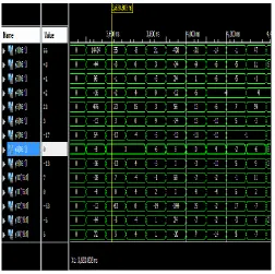
[image:6.595.313.565.357.524.2]Simulation results of proposed 2D HEVC 32 point DCT using Scalable Approximation architecture is given in Fig 13. The variables y1,y2,…y32 represents the output values. The hardware simulation is done in Xilinx Spartan 3E Field-Programmable Gate Array (FPGA), using the programming software ISE 14.2.
Fig -13: Simulation result of proposed 2D HEVC 32 point DCT using Scalable Approximation method
6.1 Performance Analysis
The optimization is mainly focused in reducing the hardware complexity and the execution time. The device utilization summary of the existing and the proposed system is given in Table 2. From Table 2 it is clear that in the proposed system,
the ‘number of slices’ and ‘total no. of 4 input LUTs’ have reduced. Delay also reduced from 4.496 ns to 4.283 ns.
Table -2: Device Utilization Summary of Existing and Proposed systems
Logic utilization Existing Proposed
No. of slices 20920 14796
No. of slice FFs 3478 17542
Total no. of 4 input LUTs 35664 19432
No. of bonded IOBs 646 1066
Total utilization 60708 52836
The percentile of hardware efficiency and delay reduction are shown in Table 3. The proposed system produced a hardware reduction of 12.93% from the existing system and delay got reduced by 4.73%. Graphical representation of the design parameters is shown in Fig 14 and Fig 15.
Table -3: Comparison of Hardware Utilization and Delay Reduction of Existing and Proposed Systems
Parameters Existing Vs. Proposed System Hardware
Efficiency 12.93%
Delay Reduction 4.73%
[image:6.595.39.292.399.650.2]0 10000 20000 30000 40000 50000 60000 70000 Slices Slice FFs 4 input LUTs Total EXISTING PROPOSED
Fig -14: Device Utilization Graph of the Two Systems
4.1 4.2 4.3 4.4 4.5 Delay(in ns) Existing Proposed
Fig -15: Delay Analysis of the Two Systems
7. CONCLUSIONS
[image:6.595.344.536.572.665.2]© 2017, IRJET | Impact Factor value: 5.181 | ISO 9001:2008 Certified Journal | Page 1592 reduced the computational complexity as the proposed
system involves only adders. 8 point DCT for both the existing and proposed system is implemented in Spartan 3E FPGA. The proposed system obtained a hardware efficiency of 12.93% and delay is reduced by 4.73%.
REFERENCES
[1] E. Kalali, A. C. Mert, I. Hamzaoglu, “A Computation and Energy Reduction Technique for HEVC Discrete Cosine Transform,” IEEE Trans. on Consumer Electronics, vol.62, no 2, pp. 166-174, May 2016.
[2] M. T. Pourazad, C. Doutre, M. Azimi, P. Nasiopoulos, “HEVC: The New Gold Standard for Video Compression,” IEEE Consumer Electronics Magazine, July 2012.
[3] J. Vanne, M. Viitanen, T.D. Hämäläinen, A. Hallapuro, “Comparative Rate-Distortion Complexity Analysis of HEVC and AVC Video Codecs”, IEEE Trans. on Circuits and Systems for Video Technology, vol. 22, no. 12, pp.1885-1898, Dec. 2012.
[4] E. Ozcan, E. Kalali, Y. Adibelli, “A Computation and Energy Reduction Technique for HEVC Intra Mode Decision,” IEEE Trans. On Consumer Electronics, vol.60, no.4, pp.745-753, Nov. 2014.
[5] G. Pastuszak “Hardware Architecture for the H.265/HEVC Discrete Cosine Transform,” IET Image Processing, vol. 9, no. 6, pp. 468-477, June 2015.
[6] P. K. Meher, S. Y. Park, B. K. Mohanty, K. S. Lim, C. Yeo, “Efficient Integer DCT Architectures for HEVC,” IEEE Trans. On Circuits and Systems for Video Technology, vol.24, no.1, pp. 168-178, Jan. 2014.
![Fig -1: HEVC 2D DCT Hardware [1]](https://thumb-us.123doks.com/thumbv2/123dok_us/8159857.805363/1.595.311.557.344.500/fig-hevc-d-dct-hardware.webp)
![Fig -2: Column butterfly structure [1]](https://thumb-us.123doks.com/thumbv2/123dok_us/8159857.805363/2.595.313.555.548.722/fig-column-butterfly-structure.webp)
![Fig -6: Reconfigurable architecture for N = 8, 16, and 32 [6]](https://thumb-us.123doks.com/thumbv2/123dok_us/8159857.805363/4.595.44.284.162.352/fig-reconfigurable-architecture-for-n-and.webp)
![Fig -10: Block diagram of the DCT for N=16 [7]](https://thumb-us.123doks.com/thumbv2/123dok_us/8159857.805363/5.595.302.556.481.697/fig-block-diagram-dct-n.webp)