Stability and Leakage Analysis of a Novel PP Based 9T
SRAM Cell Using N Curve at Deep Submicron Technology
for Multimedia Applications
Shilpi Birla1*, Rakesh Kumar Singh2, Manisha Pattanaik3
1Department of Electronics and Communication
(ECE), Sir Padampat Singhania University (SPSU), Udaipur, India
2Department of Electronics and Communication
(ECE), Bipin Tripathi Kumaon Institute of
Technology (BTKIT), Dwarahat Almora, India
3VLSI Group
, Atal Bihari Vajpayee Indian Institute of
Information Technology & Management (ABV-IIITM), Gwalior, India
E-mail:*[email protected]
Received July 22, 2011; revised August 10, 2011; accepted August 17,2011
Abstract
Due to continuous scaling of CMOS, stability is a prime concerned for CMOS SRAM memory cells. As scaling will increase the packing density but at the same time it is affecting the stability which leads to write failures and read disturbs of the conventional 6T SRAM cell. To increase the stability of the cell various SRAM cell topologies has been introduced, 8T SRAM is one of them but it has its limitation like read dis-turbance. In this paper we have analyzed a novel PP based 9T SRAM at 45 nm technology. Cell which has 33% increased SVNM (Static Voltage Noise Margin) from 6T and also 22% reduced leakage power. N curve analysis has been done to find the various stability factors. As compared to the 10T SRAM cell it is more area efficient.
Keywords: N Curve, Scaling, SVNM (Static Voltage Noise Margin), Leakage Power, 9T SRAM Cell
1. Introduction
The high demand of increasing packaging density and low power SRAMs for multimedia applications leads to the problem of data stability. As ultra low power supply voltages suppresses power consumption, gate leakage and stand by current which results in increase of life time of battery. Various Read & Write assist methods were introduced to enhance the write margin and read stability of 6T Cells. Some of the techniques are CVDD (Cell Vdd) adjustment, CVSS (Cell virtual ground), dual rail power supply, negative bitline etc. But still the voltage of the conventional 6T SRAM cannot be reduced beyond 0.6 V for successful operation. Various topologies of SRAM cell has been introduced, 7T SRAM cell in which a read static noise margin is achieved by cutting off a pull down path during read operation but has limited write capability due to single end write operations [1]. 8T SRAM cell which is one of the popular topology which increases the stability but has its own limitation. In this paper the limitation of 8T has been removed and alternative topologies have been discussed to increase the
stability [2]. Although other 9T SRAM cell as in [3] is also been discussed but it suffers from read disturbance. As far as best of my knowledge this cell has not been reported yet.
In section II various factors of SRAM functional Mar- gins has been reported. In section III the novel PP based 9T SRAM cell has been explained in detail. In section IV N curve has been discussed. In section V the analysis of various stability parameters with respect to Vdd and temperature has been discussed. In section VI the leak-age power of the proposed cell has been discussed and in the end conclusion.
2. SRAM Functional Margins
SRAM functional margins are determined by three SRAM design Parameters: static noise margin (SNM), write margin (WRM), and cell current (Icell). Since all of them strongly depend on operating voltage (VDD), tran-sistor channel length (Lg), and width (Wg). So the cell stability depends on the amount of VT mismatch caused
S. BIRLA ET AL. 275
and operation voltage VDD as well as cell ratios: γ-ratio for write and β-ratio for read [4].
2.1. Static Noise Margin
The static noise margin (SNM) is the maximum amount of noise voltage VN that can be tolerated at the both in-puts of the cross-coupled inverters in different directions while inverters still maintain bi-stable operating points and cell retains its data [5]. In other words, the static noise margin (SNM) quantifies the amount of noise vo- ltage VN required at the storage nodes of SRAM to flip the cell data. The cell becomes more vulnerable to noise during a read access since the “0” storage node rises to a voltage higher than ground (GND) due to a voltage divi-sion along the Pass gate transistors and inverter Pull- down devices between the pre-charged BL and the GND terminal of the cell. The ratio of the transistor width of Pull-down to Passgate, commonly referred to as the β-ratio determines how high the “0” storage node rises during a read access [4] as shown in Figure 1 for con-ventional 6T SRAM cell. Due to the scaling of the device to nanometer regime, the variation of β-ratio is signifi-cantly increased. This is the primary reason for increas-ing SNM challenge in nanometer-scale SRAM. The ratio of inverter pull-down transistors (M1 or M2) and pull-up transistors (M3 or M4) also directly impacts the cell im-munity to noise. Weaker pull-up due to the variations makes the cell easier to flip as lowering its trip point of inverter, making the cell more vulnerable to noise.
When the WL is off, the SNM becomes larger than that for read access because of no rising of “0” storage node from GND level [4]. The two kinds of SNMs for data retention and read access are referred to as “hold SNM margin” and “read SNM margin” [6].
2.2. Write Margin
The cell data is written by forcing the BL pair to the dif-ferential levels of “1” and “0” while WL is asserted to allow pass gate transistors (M5 or M6) connected to the BL. The potential of the corresponding storage node is pulled down to the critical level that is dependent on the ratio of transistor strengths between M5 and M3 (or M6 and M4). This ratio is referred to as γ-ratio. In order to ensure robust write operation, the critical level has to be lowered than the trip point of connected inverter before the level of “0” written BL is reached to the end-point (e.g., GND). The write margin (WRM) is defined as the rest of potential difference between the BL level at which the data is flipped and the end-point (e.g., GND) as shown in Figure 1. If the cell data is flipped when the BL comes at X mV, where X mV is allowed to reach to the GND level, WRM is defined as XmV. As the device
sizes of Pass gate and Pull-up are scaled down to nano-meter regime, the variation of γ-ratio is significantly in-creased. That is the reason why WRM has become just as difficult as read in nanometer-scale SRAM [7].
2.3. Cell Current (Icell)
The BL discharging time takes a large percentage of the total access time. The discharging time (TBL) depends on the BL capacitance, the cell current, and the required BL discharging level (VSEN). The amount of cell cur-rent (Icell) is determined by the strength of passgate and pull-down connected in series between the BL and GND as shown in Figure 1. The higher VT settings for pass gate, pull-down, and pull-up transistors in SRAM can suppress the sub-threshold leakage but it causes not only the reduction of Icell but also increases its variation [5].
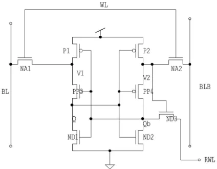
3. Proposed Novel PP Based 9T Cell
In this paper we have proposed a novel PP based 9T SRAM Cell Figure 2. In this cell one extra signal RWL is used during read operation, during read operation we keep it at gnd voltage otherwise the value remains high. The true storage nodes are separated from the two virtual storage nodes connected between the stacked PMOS. If we look at the figure we will find that there is one extra NMOS transistor is used which creates a discharging path. It is connected to the RWL. The discharging path is used such that to discharge a precharged high bitline during the read operation.
This circuit has certain advantages like it does not have read problem as the discharging path is isolated from the true storage nodes. The write ability is also not disturbed in this structure. We have used a single word-line for both the operations read and write .This cell has better stability and it is power efficient.
3.1. Detailed Structure of the Cell
[image:2.595.350.503.612.701.2]In this section, we describe our cell design in Figure 2. As mentioned previously, it is composed of two cross coupled P-P-N inverters, and data is stored in node Q and
Figure 2. Proposed PP based 9T SRAM cell.
node Qb in a complementary manner. Transistors P1, PP3, and ND1 form a P-P-N inverter and P1, PP4, ND2 form another.
ND1 provides the read current path for discharging a bitline (BL) or its complementary (BLB), depending on the stored values of Q and Qb, respectively. The source terminal of this transistor is connected to the VGND pin, which connects to the ground voltage only during the read operation. Anytime else, it stays high to curb un-necessary leakage current.V1 and V2 are located betw- een the two cascaded P-MOS transistors forming the P-P-N inverter. Q and Qb are the storage nodes .BL and BLB are bitlines while Wl is the word line as in conven- tional 6T SRAM cell.
3.2. Working of the Novel 9T Cell
3.2.1. Write Operation
During a write operation .initially in this PP based 9T SRAM Figure 2, storage node Q stores “0” while Qb stores “1”. To perform a write operation, the wordline WL is enabled and one bitline, e.g., BLB, is pulled down to ground in advance. When the supply voltage is rela-tively high (e.g., 1 V), node Qb (storing “1”) here in this case will be pulled down directly through the discharging path formed by. In turn, node Q will be charged up to complete the data-flipping process.
In general, the lower portion of our P-P-N inverter pair can be viewed as a latch consisting of PP3-ND1and PP4- ND2. In some sense, this latch takes node V1and node V2 as the pseudo supply terminals. In step 1, Qb is pulled down quickly to nearly the ground voltage at the begin-ning of the write operation since it is driven by BLB tied to strong “0”. Qb via the PMOS between them (PP3), reducing the voltage of Qb to a lower middle voltage. During this time period, PP3 and PP4 controlled by Qb still conducts weakly to pull up voltage at node Q, Due to
the coupling effect of parasitic capacitances the voltage of Qb, which is in the floating state, rises with node Q but only slightly. In step 2, the data flipping finally takes place when Q is strong enough to conduct the PDR tran-sistor to discharge Qb down to the ground voltage.
It is worth mentioning that even though such a write mechanism takes relatively longer time to accomplish the data flipping, it is still shorter than the read access time, and therefore, overall it does not introduce any operating frequency penalty. We can also further improve the cell’s write-ability by strengthening the access transistors (NA1 and NA2). It does not affect the read performance.
3.2.2. Read Operation
To perform a read operation, the wordline WL is enabled and RWL is pulled down to ground to allow bitline dis- charging. Assuming that the data stored at Q is now “0”. Since data node Q and Qb are isolated from bitline BL by PP2 and PP3 (which is between the true storage node Q) and thus the so-called read current (which is the cur- rent used to discharge a bitline) does not flow through the storage node Qb but through the bypassing ND3as indicated in Figure 2. This is the main reason why the read stability does not degrade at all in our cell. As for a 6T cell, the read current flows through the storage node directly, thereby causing read disturbance, i.e., the volt- age at data node Q will rise temporarily. This will de- grade the read stability because the cell flipping will be more likely to take place.
The pull-up transistors P1 and P2 are usually made weaker for easy write operation just like in a conven-tional 6T cell. While the pull-down transistors ND1 and ND2, forming the cell discharging paths, need to be str- onger to facilitate a larger read current and thereby a quicker access. The pass gate transistors NA1 and NA2 need to be strong enough to serve as high-conduction pa- ths between the accessed cell and the bitlines during both the read and write operations. The two pull-up transistors, PP2 and PP3, need to be slightly stronger, to compensate for the conductivity degradation of the cascaded PMOS structure linking the storage nodes (i.e., Q and Qb) and Vdd, which help contribute to a good hold SNM. Unlike a 6T cell, the pull-down transistors do not have to be strong, since they do not involve in the cell discharging paths. However, their strengths are made comparable to the cascaded PMOS structure mentioned above to ach- ieve a more balanced cell structure which could lead to a larger hold SNM.
S. BIRLA ET AL. 277
4. Stability Measurement: N Curve Analysis
Numerous analytical models of the static noise margin (SNM) have been developed to optimize the cell design, to predict the effect of parameter changes on the SNM and to assess the impact of intrinsic parameter variations on the cell stability. Furthermore, new SRAM cell circuit designs have been developed to maximize the cell stabil-ity for future technology nodes [8]. The set up for N curve is as shown in Figure 3. In an ideal case, each of the two cross-coupled inverters in the SRAM cell has an infinite gain. As a result, the butterfly curves delimit a maximal square side of maximum, being an asymptotical limit for the SNM. Therefore, scaling limits the stability of the cell. An additional drawback of the SNM is the inability to measure the SNM with automatic inline testers [4], due to the fact that after measuring the butterfly curves of the cell the static current noise margin (SINM) still has to be derived by mathematical manipulation of the measured data. An alternative definition for the SRAM read stabi- lity is based on the N-curve of the [5]. N-curve contains information both on the read stability and on the write- ability, thus allowing a complete functional analysis of the SRAM cell with only one N-curve [8].
Parameters which are find by using N curve these 4 parameters are useful for measuring the write ability and read ability of the cell.
The static voltage noise margin (SVNM)
The static voltage noise margin is the voltage differ-ence between points A and B in Figure 4 and it indicates the maximum tolerable DC noise voltage at the input of the inverter of the cell before its content changes [4]. The static current noise margin (SINM)
[image:4.595.65.277.512.706.2]The static current noise margin is defined as the maxi-
Figure 3. Set up for N curve analysis.
Figure 4. Ncurve for 6 T SRAM cell [2].
mum value of DC current that can be injected in the SRAM cell before its content changes [4]. It is given by the peak value of Iin during read operation that is be-tween points A and B in the Figure 4.
The Write Trip Voltage (WTV)
The SRAM N-curve also provides information re-garding the write ability of the cell. WTV is the voltage drop needed to flip the internal node “1” of the cell with both the bit lines clamped at Vdd [4]. It is given by the voltage difference between the second (B) and the last zero crossing point (C) in Figure 4.
The Write Trip Current (WTI)
It is the amount of current needed to write the cell when both bit lines are clamped at supply voltage equal to Vdd [5]. The peak value of Iin after the second zero crossing of N-curve gives WTI.
For better read stability, the values of SVNM, and the magnitude of SINM and hence the value of static power noise margin SPNM (product of mean of SVNM and mean of SINM) should be larger. For better write ability the value of WTV, the absolute value of WTI and hence the value of WTP (product of mean of WTV and mean of WTI) must be smaller.
5. Analysis of N Curve Metrics
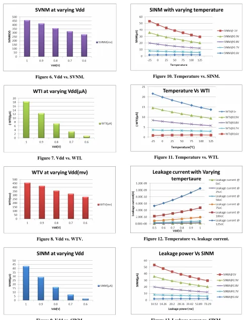
N-curve analysis has been done at 45nm technology in order for low voltage operation. Various factors of sta-bility has been analyses with the affect of temperature and voltage on them. Figure 5 shows one N curve analy-sis at Vdd = 1 V at temperature varies from –25˚C to 125˚C [2].
5.1. Effect of Power Supply (Vdd)
We have seen that there is significant affect of power supply on the 4 parameters which we have obtained from the Ncurve.As Vdd increases the stability also increases [9]. This is also been observed here that as the Vdd in-creased the SINM, WTV, SVNM and WTI the four pa-rameters has been increased as shown in the given graphs.
5.1.1. Effect on SVNM
As shown in the graph Figure 6, we see that at Vdd = 1 V it is maximum 460 mv and reduces when we go to Vdd = 0.6 V. As we know that SVNM it is the maximum DC tolerable voltage before the cell changes it contents so it means that as Vdd reduces the cell tolerance is also reduces.
5.1.2. Effect on WTI
Figure 5. N curve of 9T SRAM cell.
amount of current needed to write the cell when both bit-lines are kept at Vdd . This is the current margin of the cell for which its content changes as in (Figure 7). The ability to write a cell with both bit-lines clamped at results actually in a destructive read operation; therefore, the absolute value of WTI should be large enough to cope with the read stability requirement. On the other hand, the lower the absolute WTI is, the higher the write-trip point of the cell. It shows an exponential rela-tion with Vdd. WTI is measure at various temperatures.
5.1.3. Effect on WTV
Write-trip voltage (WTV) is the voltage drop needed to flip the internal node “1” of the cell with both the bit-lines clamped at Vdd. Write ability requires both WTI and WTV.WTV increases with Vdd. At 1 V the cell has maximum stability and it decreases drastically when the Vdd reaches to 0.6 V. As shown in Figure 8.
5.1.4. Effect on SINM
By using the combined SVNM and SINM, the read sta-bility criteria for the cell are defined properly. For exam-ple, a small SVNM combined with a large SINM will still result in a stable cell since the amount of required noise charged disturb the cell is large. At Vdd 1V we have good SINM but it reduces exponentially at Vdd = 0.6 V, as shown in Figure 9.
5.2. Effect of Temperature
As we have varied the temperature from 0˚C to 125˚C
we have seen that the SVNM and WTV is unaffected by the temperature variation but the currents i.e. the write trip current and static noise margin current has been af-fected by temperature variation. As temperature in-creases both the SINM and WTI reduces. As shown in Figures 10 and 11 respectively. The variation has been observed at varying Vdd from 1 V to 0.6 V.
6. Analysis of Leakage Current for Proposed
Cell
In this cell we have achieved 33% less leakage power with respect to 6T SRAM cell, as in this cell we have used the PMOS cell and also we used ND3 which is used to reduced the leakage power. We have seen the affect of Vdd and temperature on leakage power. As we know it depends exponential to Temperature and increases with temperature the same affect is seen here Figure 12. It also shows the effect of Vdd which shows that there is 7X increases in Leakage current when we increase the Vdd from 0.6 V to Vdd 1 V.
We have also analyzed the Leakage power with SINM as shown in Figure 13 and found that as SINM increases the Leakage power also increases which shows that with increasing Vdd the SINM increases and at the same time increasing Vdd results in increasing the leakage power [10].
7. Conclusions
S. BIRLA ET AL. 279
Figure 6. Vdd vs. SVNM.
Figure 7. Vdd vs. WTI.
Figure 8. Vdd vs. WTV.
Figure 9. Vdd vs. SINM.
Figure 10. Temperature vs. SINM.
Figure 11. Temperature vs. WTI.
[image:6.595.53.538.78.715.2]Figure 12. Temperature vs. leakage current.
been simulated at 45 nm 65% increase in SVNM compa- red to 6T SRAM cell. The cell has 33% leakage power reduction also with respect to 6T SRAM cell and in this we have not used any leakage reduction techniques. So the future expansion can be done by sizing the cell to in- crease the stability i.e. the write ability and read ability of the cell. Also power can be reduced by using various leakage reduction methods. Although the area with resp- ect to 6T has been increased but at lower technology it is comparable to 6T. The SNM measured is 380mv which can be improved by sizing the transistor widths.
8. Acknowledgements
The authors are very grateful to the respective organiza-tion for their support and encouragement.
9. References
[1] M. Sinangil, V. Naveen and A. P. Chandrakasan, “A Re- configurable 8T Ultra–Dynamic Voltage Scalable (U-DVS) SRAM in 65 nm CMOS,” IEEE Journal Solid-State of
Circuits, Vol. 44, No. 11, 2009, pp. 3163-3173.
doi:10.1109/JSSC.2009.2032493
[2] R. E. Aly and M. A. Bayoumi, “Low-Power Cache De-sign Using 7T SRAM Cell,” IEEE Transactions on
Cir-cuits and Systems II: Express Briefs, Vol. 54, No. 4, 2007, pp. 318-322. doi:10.1109/TCSII.2006.877276
[3] Z. Liu and V. Kursun, “Characterization of a Novel Nine-Transistor SRAM Cell,” IEEE Transaction of Very
large Scale Integration Systems, Vol. 16, No. 4, 2008, pp.
488-492.
[4] B. H. Calhoun and A. P. Chandrakasan “Static Noise Margin Variation for Sub-threshold SRAM in 65 nm CMOS,” IEEE Journal of Solid-State Circuits, Vol. 41, No. 7, 2006, pp. 1673-1679.
doi:10.1109/JSSC.2006.873215
[5] Y. Chung and S.-H. Song, “Implementation of Low- Voltage Static RAM with Enhanced Data Stability and Circuit Speed,” Microelectronics Journal, Vol. 40, No. 6, 2009, pp. 944-951. doi:10.1016/j.mejo.2008.11.063
[6] E. Seevinck, et al., “Static-Noise Margin Analysis of MOS SRAM Cells,” IEEE Journal of Solid-State Circuits, Vol. 22, No. 5, 1987, pp. 748-754.
doi:10.1109/JSSC.1987.1052809
[7] C. Wann, et al., “SRAM Cell Design for Stability Meth-odology,” 2005 IEEE VLSI-TSA International Symposium
on VLSI Technology, 25-27 April 2005, pp. 21-22. [8] E. Grossar, M. Stucchi and K. Maex, “Read Stability and
Write-Ability Analysis of SRAM Cells for Nanometer Technologies,” IEEE Journal of Solid-State Circuits,Vol. 41, No. 11, 2006, pp. 2577-2588.
doi:10.1109/JSSC.2006.883344
[9] S. Birla, M. Pattanaik and R. K. Singh, “Static Noise Margin Analysis of Various SRAM Topologies,” IACSIT
International Journal of Engineering and Technology, Vol. 3, No. 3, 2011, pp. 304-309.
[10] S. Birla, N. Kr. Shukla, M. Pattanaik and R. K. Singh, “Device and Circuit Design Challenges for Low Leakage SRAM for Ultra Low Power Applications,” Canadian