University of Warwick institutional repository: http://go.warwick.ac.uk/wrap
This paper is made available online in accordance with
publisher policies. Please scroll down to view the document
itself. Please refer to the repository record for this item and our
policy information available from the repository home page for
further information.
To see the final version of this paper please visit the publisher’s website.
Access to the published version may require a subscription.
Author(s): Thomas G. Dane , Philip T. Cresswell , Oier Bikondoa ,
Gemma E. Newby , Thomas Arnold , Charl F. J. Faul and Wuge H.
Briscoe
Article Title: Structured oligo(aniline) nanofilms via ionic self-assembly
Year of publication: 2012
Link to published article:
Structured Oligo(aniline) Nanofilms via Ionic Self-Assembly
Thomas G. Dane,
aPhilip T. Cresswell,
aOier Bikondoa,
bGemma E. Newby,
bThomas Arnold,
cCharl F.J.
Faul,
a,*and Wuge H. Briscoe
a,*Conducting polymers have shown great potential for application in electronic devices. A major challenge in such applications is to control the supramolecular structures these materials form to optimise the functionality. In this work we probe the structure of oligo(aniline) thin films (of
sub-µm thickness) drop cast on a silicon substrate using synchrotron surface diffraction. Self-assembly was induced through doping with an acid surfactant, bis(ethyl hexyl) phosphate (BEHP), resulting in the formation of well-ordered lamellae with the d-spacing ranging from 2.15 nm to 2.35 nm. The exact structural characteristics depended both on the oligomer chain length and film thickness, as well as the doping ratio. Complementary UV/Vis spectroscopy measurements confirm that such thin films retain their bulk electronic properties. Our results point to a simple and effective ionic self-assembly approach to prepare thin films with well-defined structures by tailoring parameters such as the oligomer molecular architecture, the nanofilm composition and the interfacial roughness.
1. Introduction
Organic semiconducting materials are becoming increasingly used in flexible electronic and optoelectronic devices.1 They
offer good charge-transport properties arising from a highly-conjugated polymeric backbone, tunable functionality afforded through simple organic-synthetic preparation and have recently been effectively prepared via simple solution processing.2 One such example that has been under
particularly intense investigation is polyaniline (PANI), which has demonstrated a high level of conductivity when treated with an acid dopant.3, 4 Previous investigations have shown a
clear link between the supramolecular structure of PANI and its conductive properties.5-10 However, control of crystalline
order is non-trivial due to the inherent polydispersity and poor solubility in common solvents of π-conjugated polymers. The interactions between the polymer chain, dopant and solvent result in a range of unpredictable structural defects such as chain-coiling and entanglement,11, 12 self-doping13 and
phase-separation of oxidation states,14 all of which inhibit the
mobility of charge through the polymer and reduce the observed conductivity.
A number of strategies have previously been employed to enhance the degree of crystallinity and solution processibility of PANI. During early investigations a strong dependence on preparation method was found, particularly with respect to the solvent used.8 With the use of certain solvents “secondary
doping” could be performed, which facilitated, to a certain degree, the uncoiling of PANI chains both in solution and in the solid state, leading to a more highly organised supramolecular structure.7 Another strategy is to control the
molecular architecture of the dopant counterion,with certain motifs giving both improved processibility and increased crystallinity. For instance, camphorsulfonic has been shown to increase the solubility of the previously unprocessible polymer in m-cresol through a process referred to as
“counter-ion induced processibility”.7, 15 This technique has been
refined through the use of counter-ions with soft alkyl tails, so-called “plasticizing dopants”.16, 17 Such methods have
yielded metaillic films with conductivites upwards of 100 S cm-1.
The highest conductivity reported for PANI (103 S cm-1)
however was achieved through self-stabilized dispersion polymerization in an aqueous phase in 2006 by Lee et al.,18
where, again, increased conductivity was reported for increased crystallinity. Despite these efforts, the theoretically predicated conductivity value of PANI is yet to be achieved. Kohlman et al proposed that as a result of the disordered nature of PANI, less than 1% of charge carriers contributed to the observed conductivity and, if all charge carriers could be accessed, the conductivity would approach that of metallic copper (~105 S cm-3).19
Another promising route to controlling the structure of organic semiconducting materials is the so-called oligomer approach, which has recently been employed effectively to achieve well-ordered supramolecular architectures and nanostructures from inorganic acid- and surfactant-doped species.20, 21 There are two features to this approach. Firstly,
Fig. 1 Chemical structures of oligo(aniline)s examined in this work
shown in the EB oxidation state (left) and when doped with BEHP to form the conducting ES state (right).
summarised in recent reviews.22, 23 Despite these studies, it
remains a challenge to control the supramolecular organisation of poly- and oligo(aniline)s. Furthermore, the majority of these studies has focused on the structural characteristics in the bulk phase.24, 25 For many applications
and processes in the electronics industry, organic materials are often required to be cast in thin films of some µm or sub-µm thickness. It is therefore important to understand the structures and their correlation with the material properties of such thin films at surfaces. A few reports have provided structural information on PANI thin films, for example, PANI Langmuir monolayers and Langmuir-Schaefer films26 and
PANI multilayers with cadmium arachidate nanoclusters.27
Some surface characterization has been performed using strongly interacting probes such as scanning probe microscopy,28, 29 providing useful local topographic and
electronic information. It is also important to obtain structual information on long-range order or crystallographic details within the thin films.
In this work we have evaluated such information of oligo(aniline) thin films of sub-µm thickness using surface diffraction performed in the X-ray reflectivity geometry. The films were prepared using a simple drop casting method, whilst the long-range order in their structures was induced exploiting oligomer self-assembly. We examined the effect of oligomer molecular architecture on the thin film structure by comparing two different oliogmeric aniline species (TANI with four monomers and OANI with eight monomers, both capped with a phenyl ring; see Fig. 1). We have also compared the structures of the films in their native EB oxidation state (without BEHP) and in the doped state (with BEHP), and found ionic self-assembly mediated by BEHP was essential in generating supramolecular assemblies with long-range order. We also found that such structural order was dependent on the thickness of the nanofilms. Our results demonstrate that the oligomer self-assembly approach (implemented with a simple drop casting method in our case) is a promising strategy to obtain well-organised thin films of sub-µm thickness, an important structural pre-requisite for achieving desired electronic properties in organic semiconducting thin films.
2. Experimental
2.1. Materials and Sample Preparation
Phenyl/phenyl-capped (Ph/Ph) TANI and phenyl/phenyl-capped octa(aniline) OANI was synthesised and characterised
according to the method described in the literature.30 The
dopant bis(ethyl hexyl)phosphate (BEHP; 97%) and tetrahydrafuran (THF; analytical grade) solvent were obtained from Sigma-Aldrich and used as received. Silicon wafers were purchased from University Wafers and cleaned by sonication for 5 minutes each in acetone, ethanol and Millipore water before rinsed with THF and dried under nitrogen flow. Solutions of the emeraldine base (EB) form of the oligomers were prepared by dissolving the oligomer in THF (10 ml) and stirring for one hour. The EB state films appeared purple. Complexes of doped emeraldine salt (ES) with BEHP were prepared by dissolving both the oligomer and BEHP in THF (10 ml) and stirring for one hour, these doped films appeared green. Such colouring of films is consistent with previous report of the EB and ES states of TANI molecules. Two thicknesses of each film were prepared and analysed. The exact mass of oligomer and dopant in each system was determined from a calculation based on the molecular volume of the system to generate (assuming complete and even coverage of the substrate) films of roughly 350 nm in thickness (henceforth referred to as “thick” films, see electronic supplementary information [ESI]) and films of roughly 35 nm (henceforth referred to as “thin” films).
The conversion of EB state oligo(aniline)s to the fully doped conducting ES state requires protonation of half of the nitrogen atoms within the chain backbone (achieved by treatement with the acid surfactant BEHP in this work). However, the remaining unprotonated nitrogen atoms are basic and can be protonated by further dopant molecules. As such it is useful to define a doping ratio to express the surfactant content within the complex. The abbreviation oligoANI(BEHP)x is used, where x is the doping ratio and corresponds to the fraction of protonated nitrogen atoms relative to the total number of nitrogen atoms within the oligomer chain.31
All films were prepared according to the following drop casting method. A clean piece of silicon (100) wafer with native SiO2 surface layer (~ 10 × 10 mm) was placed inside a
glass vessel which contained a small open vial of THF solvent (~ 10 ml). This chamber was then left for 20 minutes to allow the substrate surface to become saturated with solvent, thus facilitating the droplet wetting. Then 40 µl of oligomer solution of certain concentration was dropped to fully cover the substrate surface and then allowed to evaporate for 1 hour inside the chamber in the THF-vapour saturated atmosphere. The enclosed, solvent-rich atmosphere allowed for controlled evaporation of the solvent droplet as a means to reduce solvent drying effects and to facilitate self-assembly. This technique has been shown to greatly improve the self-organization of organic molecules in thin films.32-34
2.2. Characterisation Methods
Atomic force microscopy (AFM) imaging was performed uisng a Veeco Nanoscope III in amplitude modulation (AM) mode (silicon cantiliever from Budget Sensors; tip diameter ~ 10 nm; spring constant k ~ 40 N m-1). To determine the film
[image:3.595.45.283.64.148.2]Detector
Synchrotron radiation
θ
fθ
iQ
Sample
k
ik
fk
fFig. 2 Scattering geometry for surface diffraction measurements performed at BM28, ESRF (France) and I07, Diamond (UK). Incident and reflected angles are varied (where θi = θf = θ) and the reflected
intensity of radiation is recorded. The momentum transfer Q is defined as
Q = 4πsinθ/λ.
performed across a large area (typically ~ 50 × 50 µm) to establish the depth of the trough, which is taken as the thickness of the film. To confirm the steel had not damaged the surface of the silicon, scratch profiles using both stainless steel and PTFE coated blades were compared. No noticeable difference was observed. In some instances (see Results & Discussion) dewetting occured leaving regions of bare silicon surface. In these cases it was not necessary to scratch the surface.
Variable-angle ellipsometric measurements of the thickness of organic layer were performed by Dr R. Jacobs (University of Oxford, UK) on a Picometer ellipsometer (Beaglehole Instruments, Wellington, New Zealand) equipped with a HeNe laser at 632.8 nm.Solid-state transmission UV/Vis spectra of films were recorded on a Perkin-Elmer Lambda-35 spectrometer over the wavelength range λ = 200 – 1100 nm. Films were prepared by systematically drop casting material onto a quartz plate until a suitable absorbance was observed (Amax = 0.25 – 1.5). Data were normalized to Amax which
invariably occured at wavelength λ = 200 nm. Surface diffraction measurements on “thick” films performed in the X-ray reflectivity geometry were carried out on the XMaS beamline (BM28) at the European Synchrotron Radiation Facility (ESRF), Grenoble, France.35 Monochromatic X-ray
radiation of energy E = 10 keV (λ = 1.24 Å) was used, defined to a beam size of height 200 µm and width 550 µm. Specularly reflected intensity was recorded as a function of incident angle using an avalanche photodiode detector (See Fig. 2 for experimental scattering geometry). Data are presented as relative reflectivity as a function of the wavevector transfer Q=4πsinθ/λ.
Data were extracted using software programmed by Oleg Konovalov at beamline ID10B at ESRF and analysed using IgorPro®. Surface diffraction measurements on “thin”
oligomer films were peformed on beamline I07, Diamond Light Source, UK. Monochromatic X-ray radiation of energy
E = 20 keV (λ = 0.62 Å) was used, defined to a beam size of height 130 µm and width 320 µm, and the specular diffraction was collected using a Oxford Cyberstar X1000 scintillator detector. In both cases, data were corrected at low incident angles where the footprint of the beam was greater than the
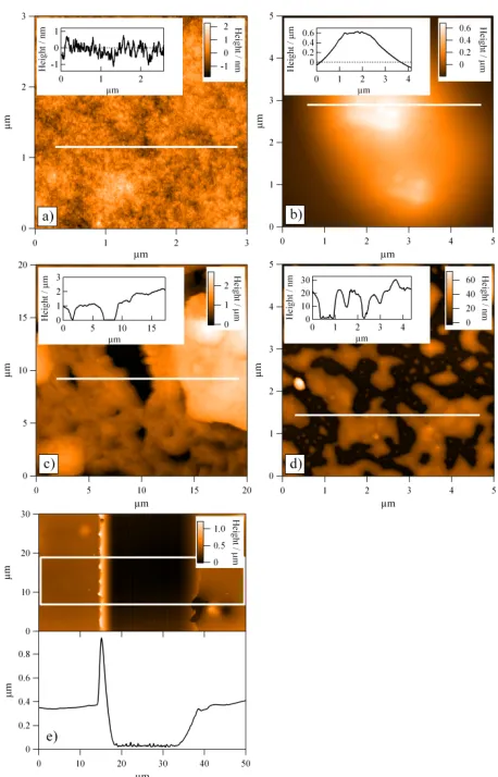
Fig. 3 AFM micrographs with inset line profiles; a) TANI(BEHP)0.5 “thick” film demonstrating low surface roughness; b) larger aggregates
found on the surface of TANI(BEHP)0.5 “thick” film; c) OANI(BEHP)0.5
“thick” film displaying high surface roughness; d) TANI(BEHP)0.5 “thin”
film displaying significant dewetting of material; e) example of scratch
profiling as performed on TANI(BEHP)0.5 “thick” film, white box
indicates region averaged for line profile.
sample.36 The diffraction peak Q positions and full widths at
half maximum (FWHM) obtained from the surface diffraction measurements were determined through a peak-fitting routine in IgorPro® software (using a cubic function to fit the background reflectivity curve and a Voigt function to fit the Bragg diffraction peak).
3. Results & Discussion
3.1. Film Topography
[image:4.595.313.542.61.418.2] [image:4.595.58.280.69.203.2]When doped with BEHP at both ratios (x = 0.5 and 1.0) the TANI “thick” films yielded much smoother films with a root mean squared (RMS) roughness of 0.4 nm (Fig. 3a) over large areas. This low roughness is evident from the line profile shown in the inset of Fig. 3a, with the corresponding profiling location indicated with a white horizontal line in the main figure. We ascribe the low roughness to the fact that the complex has much greater solubility in THF and as such is not so prone to rapid precipitation as observed for the pure oligomers. Amongst these smooth regions however were isolated deposits, likely due to the rapid local evaporation of the volatile solvent. One such example is shown in Fig. 3b, which was taken on the same sample as Fig. 3a but from a different area. These features were large – up to ~500 nm in height above the surface of the film. Overall, the TANI(BEHP)0.5 thick films displayed large areas with low
roughness, with isolated islands of deposits. Upon increasing the doping ratio, the TANI(BEHP)1.0 film displayed very
similar topographic characteristics with good surface coverage but with long-range height fluctuations (see ESI).
Unlike the TANI system, OANI(BEHP)0.5 “thick” films did
not display such good quality films, with AFM micrographs (see Fig. 3c) revealing patchy coverage. Bare silicon substrate can be seen in the AFM image as dark regions. This result can be attributed to the lower solubililty of the OANI oligomer in THF as compared with TANI.
All of the “thin” oligomer films (TANI and OANI) displayed significant dewetting into domains of thin films with height variations 10 – 50 nm (Fig. 3d and the inset line profile) with isolated larger aggregates (> 200 nm in height) interspersed across the the sample surface, one of which is seen as a bright spot on the left hand side of the figure. The thickness of films was determined using both AFM and ellipsometry (data presented Tables S1 and S2 of ESI, respectively), with the results summarised in Table S2 of ESI. An example of the AFM scratch profiling of the trough is shown in Fig. 3e. The sharp peak on the left hand side of the line profile is due to the displacement of material during scratching. By taking the image over a sufficiently large area, we are able to identify the smooth region of the film and then take the thickness of the film as the height difference between the bottom of the trough and the smooth region. Such AFM profiling reveals the film thickness locally, and we have found some variations in the thickness at different regions of the film. The thickness values obtained by ellipsometry measurements would be an average of such variations owing to a relative large footprint area that is sampled.
From the above observations, it is evident that the films doped with BEHP were smoother and with better surface coverage than the films without BEHP, owing to improved solubility. The film thickness was nonuniform across the whole film, and the “thick” and “thin” films had thickness in the range 150 – 500 nm and 10 – 50 nm respectively (c.f. Table S1). In the discussion below, the dependency of the structure of the films on the film thickness will be highlighted.
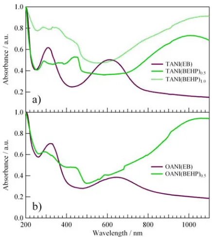
Fig. 4 Solid state UV/Vis spectra for oligo(aniline)s in the EB oxidation
state (purple) and oligo(aniline)-dopant complexes (green).
3.2 UV/Vis Spectroscopic Characterisation
UV/Vis spectra for all oligomer films (Fig. 4) were consistent with those previously reported in the literature.21 For the pure
EB TANI and OANI oligomer films, two characteristic maxima were observed at around λ = 320 nm and 620 nm, with a slight difference in the peak positions between these two oligomers. All BEHP doped films displayed the typical “polaron band”, which is present beyond λ ~ 800 nm in the long wavelength region of the examined UV/Vis range. This absorbance indicates the presence of the charged dication radical species within the oligomer backbone, and thus the doped semiconductive state. Our UV/Vis results, along with the visual observation of the colouring of the thin films, demonstrate that the preparation method used allows for complete complexation of the phosphate dopant with the oligomers. It should be noted that the UV/Vis measurements were performed using quartz as the substrate, whilst the AFM and X-ray diffraction measurements (see later) used silicon. We have assumed that the substrate would not have a significant effect on the electronic properties of the film, consistent with our visual observation that, both on quartz and silicon, the undoped EB films appeared purple and the BEHP doped films appeared green.
3.3. Oligomer Thin Film Structure by Surface X-Ray Diffraction
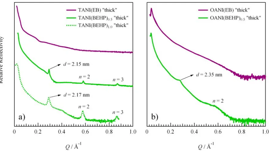
[image:5.595.311.529.64.308.2]Fig. 5 Surface diffraction data from a) TANI “thick” and b) OANI “thick” film samples. Pure EB state oligomers (purple curves) show no diffraction
features indicating that there is no long-range structure. When treated with BEHP, all oligomer films (green curves) display diffraction features corresponding to multilayer organisation of molecules lying parallel to the underlying substrate. Lamellar d-spacing values are indicated with arrows.
the film along the direction perpendicular to the substrate. Reflectivity curves for the all doped “thick” species display a similar decay in intensity as a function of Q characteristic of a rough interface. However, in all cases Bragg peaks are present arising from diffraction from lattice planes parallel to the surface. The number of the Bragg peaks observed from different samples ranges from 2-4, corresponding to the diffraction order n = 1, 2, 3, …. The Q values for these peaks invariably obey the ratio 1:2:3…, indicative of the formation of a lamellar structure in the films. The Q position of diffraction peaks is related to the periodic distance between planes of lamellae within the lattice, referred to as the d -spacing, which can be calculated using the Bragg equation,
d = 2π/Q. The calculated d-spacing values for all the doped “thick” films are listed in Table 1.
In addition to considering the peak positions, the broadening of the diffraction peaks, as assessed by their width, was also evaluated to provide further information on the nature of the ordered regions within the nanofilms. There are two contributions to this peak broadening: finite crystalline domain size and fluctuations of the lattice spacing. Firstly, it has been shown that the full width at half maximum (FWHM), ∆Q (in Å-1), of a Bragg diffraction peak
is inversely proportional to the size of the crystalline domain or coherence length (La) through the following equation:37
Q K La
∆
=2π (1)
where is the wavelength of radiation and K is a shape factor of order unity, a value to correct for the shape of particles or crystallites.
Furthermore, peak broadening can also occur due to fluctuations of the lattice spacing about a mean value, the so-called paracrystalline disorder.38 Bragg peaks observed in surface
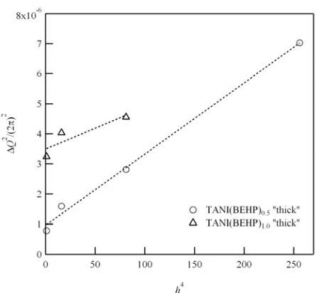
diffraction can be analysed to determine the relative contributions of these two effects39 as was recently demonstrated by Lilliu et al.40 By plotting the peak broadening (∆Q2/(2π)2 as a function of
the order of diffraction (h4) for a plane of Miller indices (h00),
the contributions to peak broadening from correlation length and paracrystalline disorder can be separated. For our lamellar structure, h = 1, 2, 3,… By fitting a linear function of the form
y = mx + c defined in Eq. 2 below, the correlation length La can be determined from the intercept c, and the disorder parameter
g(h00) from the gradient m:40
( )
( )
2 2 for 1,23... 200 =
∆
= Q h
y h
π (2a)
( )
2 2 2 12 a
c
L Q c= ∆ =
π (2b)
( )
(
)
( )
... 3 2 , 1 for
2 00
4 2
00 =
= h
d g m
h h
π (2c)
4
h
x= (2d)
[image:6.595.81.520.79.326.2]a measure of the statistical deviation of the lattice spacing fluctuations from the main lattice spacing value d.38
Table 1 Summary of structural information for oligoANI(BEHP)x“thick”
film samples determined through peak fitting routines.
Sample TANI(BEHP)0.5 TANI(BEHP)1.0 OANI(BEHP)0.5
d-spacing / nm 2.15 2.17 2.35
Structure Lamellar Lamellar Lamellar Coherence
length La /nm 102 54 7
No. of layers 48 25 3
Disorder
parameter g(100) 0.058 0.051 N/A
a Determined form FWHM of first Bragg reflection only.
It must be noted that at least three orders of reflection must be observed in order to accurately retrieve information from this analysis,38 and as such this analysis could only be applied
to the TANI(BEHP)x “thick” samples and not the OANI(BEHP)0.5 “thick” sample.
The “thick” TANI(BEHP)0.5 film displays very sharp Bragg
peaks in the reflectivity curve indicating a well-ordered structure over a long range. Four diffraction peaks are present, with the second, third and fourth peaks being the higher order
n = 2, 3 and 4 reflections, respectively (the Q range displayed in Fig. 5a shows only the first three orders of diffraction), corresponding to a d-spacing of 2.15 nm. This indicates that there is a very well-defined lattice spacing displaying a multilayered lamellar structure along the direction perpendicular to the substrate. Such peaks were absent from the undoped TANI sample.
The linear fitting for TANI(BEHP)x “thick” samples is shown in Fig. 6. Note that four orders of reflections were observed for the x = 0.5 sample which allows for a more accurate fit than for the x = 1.0 samples. The results of this analysis are listed in Table 1. In the case of TANI(BEHP)0.5,
the corrected coherence length (after removing the contribution of paracrystalline disorder) was found to be approximately 102 nm which corresponds to around 50 layers of lamellae. The disorder parameter for this system was also extremely low at ~0.06. From the AFM and surface diffraction results it is clear the air-film interface is rough. Additionally, it is well established in the literature that the native silicon oxide surface layer does not direct surface crystallisation and in fact prevents the formation of structure close to the surface. These observations therefore indicate that a large ordered domain exists within the middle of the thin film, whilst the disordered interfacial domains below and above prevent the proliferation of self-organisation through the entire film. The bulk phase lattice structure of TANI(BEHP)0.5 has been
proposed by Wei et al from Small-Angle X-ray Scattering (SAXS) experiments.21 Comparing our surface diffraction
data with those from bulk scattering measurements provides further insight into the nature of lamellar structure observed here. The 2-dimensional parallelogram lattice (constants
a = 2.35 nm, b = 2.7 nm and γ = 80°), consisting of layers of
two TANI units spearated by a bilayer of interdigitated alkyl tails displays an interlayer distance of 2.20 nm, a value close to the lameller d-spacing observed in surface diffraction
Fig. 6 Peak broadening of lamellar reflections as function of diffraction
order for TANI(BEHP)x “thick” film samples (x = 0.5 and 1.0).
measurments of 2.15 nm. It can therefore be assumed that the Bragg peaks observed in these experiments for certain thin films are attributed to the (h00) reflections along the a lattice
vector. Assuming the lattice structure is similar to that of the bulk phase, the b lattice parameter corresponds to the length of the TANI molecule (2.75 nm) and the c lattice parameter to the π−π stacking distance (0.36 nm). This gives rise to a unit cell with an approximate volume of 2.13 nm3 which is roughly
twice the molecular volume of the TANI(BEHP)0.5 complex
(1.1 nm3 as determined in ref. 21). This implies that two
TANI(BEHP)0.5 complexes are present in the unit cell. A
graphical representation of this possible “bilayer” lamellar structure is shown in Fig. 8.
An alternative to this “bilayer” structure would be alternating single layers of TANI and BEHP in a “monolayer” type structure (see ESI Fig. S4a), however, this would give rise to a lamellar d-spacing of approximately 1.5 nm, significantly smaller than reflections observed in these investigations. Additionally, we also argue that adopting the bilayer stucture allows for more efficient space-filling, with alkyl tails packed into a more thermodynamically stable structure with optimal van der Waals interaction between the chains.
If this model is assumed to be correct for the thin film phase, it can be seen that the lamellar packing when confined to this regime is more compact, possibly due to the formation of a more symmetrical unit cell in comaprison with the bulk lattice. Additionally, as XRR configuration probes the electron density perpendicular to the surface it is apparent from the observation of (h00) reflections that the a lattice
vector must be aligned roughly parallel to the surface normal within the ordered regions. Such alignment is consistent with that previously reported for polythiophene derivatives where covalently bonded alkyl side-chains encourage self-organisation.40-43
The TANI(BEHP)1.0 system displays a lamellar d-spacing
[image:7.595.46.286.119.213.2]Fig. 7 X-ray reflectivity curves for oligoANI(BEHP)x “thin” film
samples. In all cases the Bragg diffraction features seen for the “thick” films are absent.
that the lattice structure (at least along the a lattice vector) is
not altered by the greater volume fraction of surfactant. This observation is compatible with the UV/Vis spectra, which does not vary greatly between the two systems. The coherence length however is much smaller, roughly half that of the x = 0.5 complex at 54 nm (~25 layers). Previous literature has reported that the lamellar spacing of PANI treated with a poly(ethylene oxide) dopant could be systematically and significantly increased by varying the amount of dopant.44
Such a result was not observed in this experiment and suggests that the TANI(BEHP)1.0 complex has not been
achieved and instead domains of the x = 0.5 structure exist plasticised by excess uncoordinated BEHP. However, it has been reported for double-tailed surfactant-polypeptide complexes that increasing the volume fraction of surfactant does not lead to a swelling of lattice sructure, rather the surfactants are able to pack more densly within the original supramolecular structure.45 Alternatively, the increase of
surfactant volume fraction could lead to an expansion along another lattice vector to accomodate additional surfactant tails. It is not possible to elucidate which scenario is most accurate for this system with the present data and further investigations will be carried out in the future.
In the case of the OANI(BEHP)0.5 “thick” film two broad,
diffuse peaks are observable, as shown in Fig. 5b. The Q
positions of the peaks have a ratio of 1:2, corresponding to a lamellar organisation with a d-spacing of 2.35 nm. The peaks appear very broad with low intensity, which indicates that the coherence length is much smaller and that the lamellar structure is not very well-defined. A correlation length of 7 nm was determined from the peak width for the first reflection. Whilst the paracrystalline correction has not been applied to this result it is evident that the domain size is significantly smaller than that seen for the tetrameric
TANI
BEHP
2.15 nm
Fig. 8 Proposed structure for the lamellar organisation of molecules in the
nanofilms of TANI(BEHP)0.5 complex. The observed d-spacing of
2.15 nm determined through surface diffraction may contain bilayers of TANI separated by interdigitated alkyl tails from the BEHP dopant. This structure is consistent with the bulk phase lattice though with a more tightly packed multilayer arrangement.21
complexes. Both the increase in multilayer d-spacing and smaller domain size can be attributed to the nature of the OANI octamer. By increasing,in this case doubling, the chain length of oligomer, the molecular backbone becomes more flexible through rotation of the phenyl-amine-phenyl bonds. We postulate that the enhanced molecular flexibility associated with longer OANI hinders the formation of tightly packed layers, and gives rise to less well defined organisation or order in the thin film structure. This leads to an increase in the lamellar spacing and broadening of diffraction peaks as observed, when compared to that of the TANI(BEHP)0.5
system.
The BEHP-doped “thin” oligo(aniline) films were also examined with X-ray surface diffraction. From the diffraction curves shown in Fig. 7 it is evident that the structures present in the “thick” films is absent in thinner films. The TANI(BEHP)1.0 “thin” film displays a slight peak at roughly
disordered air-film interface is too great in the case of the "thin" film samples for self-organised structures to occur. In summary, well-defined lamellar morphologies of aniline oligomer-surfactant complexes were found to form after drop casting and solvent annealing which yielded diffraction features not seen for pure oligomers (EB oxidation state). Moreover, the lamellar organisation was found to differ from the previously reported bulk phase when confined to the thin film phase. In the case of “thick” films, the presence of sharp Bragg peaks in the TANI(BEHP)0.5 system revealed that it
was highly ordered with an inter-layer distance of 2.15 nm. By contrast, the OANI system produced broader and less intense Bragg peaks arising from a less well-defined organisation with a spacing of 2.35 nm, confirming that as the oligomer chain length increase the properties of the material approach that of the polymer. UV/Vis spectra confirmed that complexes in the solid state had been thoroughly doped to yield the conductive species. Together these results suggest that order can be induced through simple preparation techniques and should lead to good anisotropic conductive properties – a function which will be investigated in a future study.
4. Conclusion
In conclusion, our results show the generation of highly ordered doped oligo(aniline) films, which depend on a number of factors: 1) the presence of the dopant (BEHP in our case) is necessary to induce self-assembled ordered structure, 2) the organisation of the formed structures depend on the molecular architecture of the oligomers (i.e., TANI vs. OANI), and 3) that drop cast films must be of a certain thickness in order to overcome the disorder introduced from the rough air-flm and film-substrate interfaces to form ordered structures. As our surface diffraction measurements only examine the surface structure in the direction prependicular to the substrate, our data show that these multilayers are oriented parallel to the substrate plane. Based on our observations, we suggest a lamellar structure of the oligomer nanofilms, as schematically shown in Fig. 8. Our results highlight the importance of the mentioned parameters and how they may be tailored to obtain structured nanofilms, which have potential applications in thin film electronic and optoelectronic devices.
5. Acknowledgements
We are indebted to many helpful discussions with Dr. Emyr MacDonald and Samuele Lilliu at University of Cardiff regarding the interpretation of the diffraction data. The TANI and OANI oligomers were synthesised and kindly provided by Zhecheng Shao. The ellipsometry measurements of the film thickness were performed by Dr. Robert Jacobs at the Surface Analysis Facility, Oxford University. Georgia Pilkington helped to collect the diffraction data in Fig. 8. TGD is funded by an EPSRC DTA studentship. WHB would like to acknowledge financial support from the Engineering and Physical Science Research Council (EPSRC) (EP/H034862/1) and the European Research Council (ERC). CFJF thanks the University of Bristol for support. We also thank the European
Synchrotron Radiation Facility (ESRF) and the Diamond Light Source (UK) for access to synchrotron X-ray sources.
6. Notes and references
a School of Chemistry, University of Bristol, Cantock’s Close, Bristol BS8
1TS, UK.
bXMaS, The UK-CRG Beamline at the ESRF. B.P. 220, 38043 Grenoble
CEDEX 09, France and Department of Physics, University of Warwick,
Gibbet Hill Road, Coventry, CV4 7AL, UK
cDiamond Light Source Ltd., Diamond House, Harwell Science and
Innovation Campus, Didcot, Oxfordshire. OX11 0DE, UK * Corresponding authors; email: [email protected]; [email protected]
† Electronic Supplementary Information (ESI) available: details of solution preparation, summary of film thickness determination using both AFM and ellipsometry, additional AFM micrographs and details of peak fitting routines used to characterise the Bragg peaks observed in surface diffraction.
1. S. R. Forrest and M. E. Thompson, Chem. Rev., 2007, 107, 923-925. 2. J. M. D’Arcy, H. D. Tran, V. C. Tung, A. K. Tucker-Schwartz, R. P.
Wong, Y. Yang and R. B. Kaner, P. Natl Acad. Sci. USA,
2010, 107, 19673-19678.
3. A. G. Macdiarmid, J. C. Chiang, A. F. Richter and A. J. Epstein,
Synth. Met., 1987, 18, 285-290.
4. J. C. Chiang and A. G. Macdiarmid, Synth. Met., 1986, 13, 193-205. 5. Z. H. Wang, E. M. Scherr, A. G. MacDiarmid and A. J. Epstein,
Phys. Rev. B, 1992, 45, 4190.
6. J. Joo, Z. Oblakowski, G. Du, J. P. Pouget, E. J. Oh, J. M. Wiesinger,
Y. Min, A. G. MacDiarmid and A. J. Epstein, Phys. Rev. B,
1994, 49, 2977.
7. A. G. Macdiarmid and A. J. Epstein, Synth. Met., 1994, 65, 103-116. 8. J. P. Pouget, M. E. Jozefowicz, A. J. Epstein, X. Tang and A. G.
Macdiarmid, Macromolecules, 1991, 24, 779-789.
9. E. J. Oh, Y. Min, J. M. Wiesinger, S. K. Manohar, E. M. Scherr, P. J. Prest, A. G. MacDiarmid and A. J. Epstein, Synth. Met., 1993,
55, 977-982.
10. K. R. Cromack, M. E. Jozefowicz, J. M. Ginder, A. J. Epstein, R. P. McCall, G. Du, J. M. Leng, K. Kim and C. Li,
Macromolecules, 1991, 24, 4157-4161.
11. Y. Xia, A. G. MacDiarmid and A. J. Epstein, Macromolecules, 1994,
27, 7212-7214.
12. Y. N. Xia, J. M. Wiesinger, A. G. Macdiarmid and A. J. Epstein,
Chem. Mater., 1995, 7, 443-445.
13. S. M. Long, K. R. Brenneman, A. Saprigin, R. S. Kohlman, A. J. Epstein, M. Angelopoulos, S. L. Buchwalter, A. Rossi, W. Zheng and A. G. MacDiarmid, Synth. Met., 1997, 84, 809-810. 14. J. Y. Shimano and A. G. MacDiarmid, Synth. Met., 2001, 123,
251-262.
15. Y. Cao, P. Smith and A. J. Heeger, Synth. Met., 1992, 48, 91-97. 16. T. E. Olinga, J. Fraysse, J. P. Travers, A. Dufresne and A. Pron,
Macromolecules, 2000, 33, 2107-2113.
17. B. Dufour, P. Rannou, P. Fedorko, D. Djurado, J.-P. Travers and A. Pron, Chem. Mater., 2001, 13, 4032-4040.
19. R. S. Kohlman, A. Zibold, D. B. Tanner, G. G. Ihas, T. Ishiguro, Y. G. Min, A. G. MacDiarmid and A. J. Epstein, Phys. Rev. Lett., 1997, 78, 3915-3918.
20. H. Zengin and G. KalaycI, Mater. Chem. Phys., 2010, 120, 46-53.
21. Z. X. Wei, T. Laitinen, B. Smarsly, O. Ikkala and C. F. J. Faul,
Angew. Chem. Int. Ed., 2005, 44, 751-756.
22. Z. X. Wei and C. F. J. Faul, Macromol. Rapid Comm., 2008, 29,
280-292.
23. C. U. Udeh, N. Fey and C. F. J. Faul, J. Mater. Chem., 2011, 21,
18137-18153.
24. W. Luzny, E. J. Samuelsen, D. Djurado and Y. F. Nicolau, Synth.
Met., 1997, 90, 19-23.
25. M. J. Winokur and B. R. Mattes, Macromolecules, 1998, 31,
8183-8191.
26. L. Cristofolini, M. P. Fontana, O. Konovalov, T. Berzina and A. Smerieri, Langmuir, 2009, 25, 12429-12434.
27. V. Vidya, N. P. Kumar, S. N. Narang, S. Major, S. Vitta, S. S.
Talwar, P. Dubcek, H. Amenitsch and S. Bernstorff, Colloid
Surface A, 2002, 198, 67-74.
28. P. K. Ho, P. C. Zhang, L. Zhou, S. F. Y. Li and H. S. O. Chan, Phys. Rev. B, 1997, 56, 15919.
29. Y. Lee, C. Chang, S. Yau, L. Fan, Y. Yang, L. O. Yang and K. Itaya,
J. Am. Chem. Soc., 2009, 131, 6468-6474.
30. Z. Shao, P. Rannou, S. Sadki, N. Fey, D. M. Lindsay and C. F. J. Faul, Chem.–Eur. J., 2011, 17, 12512-12521.
31. Considering the TANI(BEHP)x system for example; when x = 0.5
half of the nitrogen atoms are protonated and coordinated with oppositely charged BEHP molecules, resulting in a complex involving one TANI molecule and two BEHP molecules.
When x = 1.0 all of the nitrogen atoms protonated and the
complex incorporates four BEHP molecules for every TANI molecule.
32. S. H. Kim, M. J. Misner and T. P. Russell, Adv. Mate., 2004, 16,
2119-2123.
33. G. Li, V. Shrotriya, J. Huang, Y. Yao, T. Moriarty, K. Emery and Y. Yang, Nat. Mater., 2005, 4, 864-868.
34. G. Li, Y. Yao, H. Yang, V. Shrotriya, G. Yang and Y. Yang, Adv.
Func. Mater., 2007, 17, 1636-1644.
35. S. D. Brown, L. Bouchenoire, D. Bowyer, J. Kervin, D. Laundy, M. J. Longfield, D. Mannix, D. F. Paul, A. Stunault, P.
Thompson, M. J. Cooper, C. A. Lucas and W. G. Stirling, J.
Synchrotron Radiat., 2001, 8, 1172-1181.
36. Surface diffraction data were corrected for the varying beam footprint as a function of incident angle (θ); above a certain angle θ* the beam footprint is smaller than the area of the substrate, below this angle some of the radiation does not fall on the sample and as such the total reflected intensity is not measured. This can be corrected for using the following relationship:
Ic = I0(sinθ*/sinθ) where I0 and Ic correspond to the initial and
corrected intensity of radation respectively. 37. A. L. Patterson, Phys. Rev., 1939, 56, 978.
38. R. Hosemann and A. M. Hindeleh, J. Macromol. Sci-Phys., 1995,
B34, 327-356.
39. A. Salleo, R. J. Kline, D. M. DeLongchamp and M. L. Chabinyc,
Adv. Mater., 2010, 22, 3812-3838.
40. S. Lilliu, T. Agostinelli, E. Pires, M. Hampton, J. Nelson and J. E. Macdonald, Macromolecules, 2011, 44, 2725-2734.
41. H. Sirringhaus, P. J. Brown, R. H. Friend, M. M. Nielsen, K. Bechgaard, B. M. W. Langeveld-Voss, A. J. H. Spiering, R. A. J. Janssen, E. W. Meijer, P. Herwig and D. M. de Leeuw,
Nature, 1999, 401, 685-688.
42. L. H. Jimison, A. Salleo, M. L. Chabinyc, D. P. Bernstein and M. F. Toney, Phys. Rev. B, 2008, 78, 125319.
43. D. H. Kim, B.-L. Lee, H. Moon, H. M. Kang, E. J. Jeong, J.-I. Park, K.-M. Han, S. Lee, B. W. Yoo, B. W. Koo, J. Y. Kim, W. H.
Lee, K. Cho, H. A. Becerril and Z. Bao, J. Am. Chem. Soc.,
2009, 131, 6124-6132.
44. B. Nandan, H. L. Chen, C. S. Liao and S. A. Chen, Macromolecules,
2004, 37, 9561-9570.
45. S. Junnila, S. Hanski, R. J. Oakley, S. Nummelin, J. Ruokolainen, C. F. J. Faul and O. Ikkala, Biomacromolecules, 2009, 10,