1
Faculty of Electrical Engineering,
Mathematics & Computer Science
Feasibility Study of
Frequency Doubling
using a Dual-Edge Method
R. Oortgiesen
MSc. Thesis
November 2010
iii
Abstract
The performance of integrated Frequency Synthesizers relies on a clean fixed reference frequency, which is usually derived from a crystal. Unfortunately, commercially cheap crystal oscillators are limited in the range from 20 - 50 MHz. In general, a higher reference frequency results in better noise performances for Frequency Synthesizers. Therefore it is desired to be able to double the reference frequency and at the same time preserving the clean crystal properties.
This work examines the feasibility of a low power and low noise CMOS Frequency Doubler in CMOS IC-technology. Main target speci-fications are: -151 dBc/Hz phase-noise floor, 10 kHz flicker noise corner frequency and reference spurs at the synthesizer output should be smaller than -80 dBc, within a power budget of approximately 4 mW. Within this scope a Phase-Locked Loop (PLL) has been analyzed, which showed insufficient yield for successful realization of a frequency doubler that would meet the given demands.
Next to a PLL, an alternative has been examined which relies on pass-ing through the edges of the clean reference crystal. By combinpass-ing both rising- and falling edges of the reference frequency (fref) into both rising
edges, an output frequency of 2 xfref is obtained. Main drawback of
Contents
Contents v
1 Introduction 1
1.1 Project Goal . . . 2
1.2 Specifications . . . 2
1.3 Solution Directions and State-of-the-Art . . . 3
2 PLL Exploration and Analysis 5 2.1 PLL Background . . . 5
2.1.1 PLL Dynamics . . . 6
2.2 PLL Noise Analysis. . . 6
2.2.1 VCO Phase Noise and PLL Benchmarking. . . 8
2.3 PLL Performance . . . 8
2.3.1 Specifications Revision . . . 10
2.3.2 Fit Specification in State-of-the-Art PLL Design . . . . 11
2.4 Summary . . . 12
3 Frequency Doubling 13 3.1 Idea . . . 13
3.1.1 Drawback . . . 14
3.1.2 Sources of Error . . . 15
3.2 Specifications Revision . . . 16
3.2.1 Redefinition Of Specifications . . . 17
3.3 Frequency Doubler Implementation. . . 19
3.3.1 Offset Cancellation . . . 20
3.4 Error Detection . . . 21
3.5 Error Correction . . . 24
3.6 Complete Circuit Functionality and Simulations. . . 25
3.7 Summary . . . 27
4 System Analysis 29 4.1 Linearized System Model . . . 31
4.1.1 Behavioral quantification . . . 32
4.1.2 Time Discrete Feedback . . . 33
4.2 Simulation comparison . . . 34
4.2.1 Time Continuous Model . . . 34
4.2.2 Time Discrete Model . . . 36
vi CONTENTS
5 Noise Estimation 39
5.1 Noise in Sampled Systems . . . 39
5.1.1 Cyclostationary Noise . . . 40
5.1.2 Noise Sampling . . . 40
5.2 Noise and Jitter. . . 42
5.2.1 Definitions . . . 42
5.3 Noise Estimation and Simulations. . . 43
5.3.1 Achieved Performance vs. Requested Performance . . . 48
5.4 Summary . . . 49
6 Conclusions and Recommendations 51 6.1 Conclusions . . . 51
6.2 Recommendations . . . 53
Chapter 1
Introduction
Wireless communication takes in an increasingly important role in our everyday lives. Mobile phones for example, took a flight from voice communication since its introduction mid eighties to broadband internet access today. Much of the functional complexity of such a Radio Frequency (RF) device is carried out by digital circuitry in the low-frequency baseband range. Along with digital signal processing, the analog circuitry is an essential part of the hardware since this is operating in the RF range to mix these signals to baseband to be able to convert them to digital signals [Fig. 1.1].
Baseband Section RF
Section
Figure 1.1: RF and baseband sections in an RF device.
An example of an RF section can be a radio-frequency receiver, where a stable1frequency is used to tune to a radio-frequency of interest. In nowadays
Integrated Circuits (IC) this is done by integrating a frequency synthesizer to generate a variety of stable tunable frequencies. A frequency synthesizer relies on a clean fixed reference frequency which is usually derived from a crystal and determines for a big part the performance of the frequency synthesizer.
Unfortunately, commercially cheap crystals are limited in the range of 20 - 50 MHz. For a fractionN synthesizer, a higher reference frequency al-lows to reduce the noise contribution from the sigma-delta modulator in the fractional-N synthesizer. Therefore there is the desire to double (or even better, multiply) the reference frequency and at the same time preserving the clean crystal properties.
1Stability is usually defined as long-term stable and short-term stable. The first defines its
stability over a longer period of time which ensures absolute accuracy. The second defines its spectral purity in terms of phase noise and jitter which is important to prevent down-mixing of unwanted interferer signals.
2 CHAPTER 1. INTRODUCTION
1.1
Project Goal
The goal of the project is to examine the feasibility of a low power and low noise solution for a sub-section between the fixed reference frequency (crystal) and the frequency synthesizer, with the purpose of frequency doubling (Fig.
1.2).
Frequency Synthesizer Frequency
Doubler crystal
Figure 1.2: System perspective of doubler sub-section.
1.2
Specifications
Since the frequency doubler[Fig.1.2] will act as the fixed reference frequency for the frequency synthesizer, it is not hard to imagine that the frequency doubler is not allowed to deteriorate too much in terms of noise properties compared to the crystal. This puts relatively high demands on the doubler sub-section since a crystal oscillator has naturally very good noise properties.
The input frequency, that is the clean crystal reference frequency, is assumed to range from 20 to 50 MHz (the range in which crystals are still commercially available cheaply). Based on synthesizer specifications, Catena derived require-ments for the frequency doubler as illustrated in Fig. 1.3 and given in Table
1/f corner
10kHzf
(log scale)phase noise floor
1/f
spur
(f)
10MHz
100kHz 1MHz
-151 dBc/Hz -122 dBc/Hz
1.3. SOLUTION DIRECTIONS AND STATE-OF-THE-ART 3
1.1. The doubled output frequency, thus in the range of 40 - 100 MHz, has a noise floor of -151 dBc/Hz. The 1/f corner frequency, which is usually dom-inated by the flicker noise of MOSFETS for in example buffers, should not exceed 10 kHz. Furthermore are spurious tones in the frequency spectrum are not allowed to be greater than -122 dBc. These specifications have to be met within a power budget of roughly 4 mW .
Parameter Min. Typ. Max. Unit
Output frequency 2·fin Hz
Output phase noise floor -151 -149 dBc/Hz
Output phase noise 1/f corner 10k 15k Hz
Output spurious -122 dBc
Power dissipation 4m Watt
Table 1.1: Target performance specifications.
1.3
Solution Directions and State-of-the-Art
This document first examines the feasibility of realizing a frequency doubler with the given specifications by means of Phase Locked Loop (PLL).
Next to a PLL, an alternative method that exploits both already available crystal edges is explored. The latter method has been used in front of the Σ∆ frac-N frequency synthesizer in [1] to reduce the in-band phase noise. The paper describes that both edges are combined by means of a delay element and an XOR gate, which is more recently also reported in [2]. Although [1] does not give extensive analysis and performance of the doubler circuit, it does report the need for a correction circuit to deal with the duty-cycle error that will lead to reference spurs. The duty-cycle correction (DCC) circuit as proposed in [1] is a digital solution with a resolution of 200 ps, and reports this is sufficient due to the reference spur being far beyond the loop bandwidth. It furthermore mentions that the phase noise spectrum is not affected.
This document aims to explore the feasibility of a novel doubling circuit without the use of a delay element and XOR gate. The proposed correction circuit acts as a control loop around the doubler circuit and due to its analog nature is not directly restricted to a maximum resolution. Furthermore it aims to give an more extensive analysis of the performance.
Chapter 2
PLL Exploration and Analysis
A Phase Locked Loop (PLL) has several applications, and one of them is fre-quency multiplication. This Chapter deals with the exploration of a PLL design for frequency doubling, and possibly multiplication by more than 2, to meet the specification as described in Chapter 1. Before doing so, it is instructive to first look at the basic concepts and background of the PLL to further on use it in the exploration and analysis phase.
2.1
PLL Background
The basic concept of a PLL is a feedback system that consists of a Phase Detector (PFD) and a Voltage Controlled Oscillator (VCO)[Fig. 2.1]. Its functionality is based on aligning the phase of the VCO (output) with the phase of the fixed reference frequency (input).
LPF
VCO
Φin Vin
Φout
PD
VoutFigure 2.1: Simple PLL system.
The PFD compares the phases of Vout and Vin, generating an error that varies the VCO frequency until the phases are aligned. The output of the PD,VP F D, consist next to the desired dc component to vary the VCO, of an undesired high-frequency component. This high-frequency component disturbs the control voltage Vcont and must therefore be filtered, hence the Low Pass Filter (LPF)[3].
This topology can be modified by adding divider section in its feedback path [Fig. 2.2]. When making use of the previous conclusions one can see for this case that when the phases are aligned the frequencies are equal and hence fout/N =fin. This means that the input frequency fin is actually multiplied by a factorN, givingfout =N fin.
6 CHAPTER 2. PLL EXPLORATION AND ANALYSIS
LPF
VCO
Φin Vin
Φout
PD
VoutN
1
Figure 2.2: PLL with divider in feedback path.
2.1.1
PLL Dynamics
To be able to analyze the behaviour more thoroughly it is important to look at the dynamics of the PLL. This can best be done by s-domain derivations to determine the transfer function Φout(s)/Φin(s). Where Φ denotes the excess phase. This gives insight in how the output phase tracks the input phase for slow and rapid variations (low and high frequencies). The transfer function of a type I PLL can be derived by constructing a linear model as in Fig. 2.3.
LPF
VCO
Φin Φout
PD
N
1
K
PD1
LPF
s +
1 ω VCOs
K
+
-Figure 2.3: Linear model of type I PLL.
When finding the transfer function from input Φin to Φout one can write
H(s)|closed=
KP DKV CO s2
ωLP F +s+ 1
NKP DKV CO
. (2.1)
2.2
PLL Noise Analysis
A noise model of a PLL can be made by using the linear model and include the various noise sources as shown in Fig. 2.4. At first hand, for sake of analysis, only the thermal noise of the noise sources is considered that are normally dominant, where 1/f noise is neglected. This leads to the VCO noise having a 1/f2shape due to the integrating action on the white (flat) noise. The spectra of the other noise sources stay white.
2.2. PLL NOISE ANALYSIS 7
LPF(s)
Figure 2.4: Noise model PLL.
components, hence loop phase noise, to the PLL output. The noise transfer function from VCO to PLL output is
HV CO(s) =
1 1 + 1
NKP DZLF(s)KV COs
. (2.2)
The loop phase noise are the noise contributions when one goes from divider input to PLL output. The noise transfer function from the loop phase noise can therefore be calculated as
HV CO(s) =
1
NKP DZLF(s) KV CO
s 1 + 1
NKP DZLF(s) KV CO
s
. (2.3)
Comparing (2.2) and (2.3) leads to the insight that the VCO phase noise is high pass filtered and the loop phase noise low pass filtered. Fig. 2.5shows the overall PLL phase noise transfer, where the bandwidth of the PLL is indicated byfc.
PLL loop VCO
white noise components
8 CHAPTER 2. PLL EXPLORATION AND ANALYSIS
2.2.1
VCO Phase Noise and PLL Benchmarking
In numerous studies [4], [5] it has been found that the phase noise of a VCO is systematically dependent on the important design parameters: oscillation frequency, power dissipation, and offset frequency at which the phase noise is measured. Therefore it is interesting to look at the minimum achievable phase noise produced by a VCO for a given power budget, as has been studied in [6]. For RC relaxation oscillators the minimum achievable phase noise is found to be approximated by [6]
P Nmin(∆f)≈ 3.1kT
Pmin f o ∆f 2 . (2.4)
And for ring oscillators the minimum achievable phase noise is approximated by [6]
P Nmin(∆f)≈ 7.33kT
Pmin f o ∆f 2 . (2.5)
Benchmarking PLL’s gives a measure of the quality of PLL designs. The benchmark for PLL’s that is recently introduced in [4] is the PLL Figure of Merit (FoM) and gives a measure that is typically determined by the total amount of phase noise and the power that it consumes. The PLL FoM definition as described in [4] is
F OMP LL= 10log
" σ t,P LL 1s 2P P LL 1mW # . (2.6)
Furthermore in [4] it is derived that if the loop bandwidth is chosen optimally to balance the loopnoise and VCO noise contributions, then:
F OMP LL∝F OMloop+F OMV CO. (2.7) This last statement suggests that the design quality of the PLL loop and the VCO are equally important. conditionally true if the PLL bandwidth is op-timized. When going back to Fig. 2.5 one can see that the corner frequency, fc, is chosen to be there where the 1/f2 VCO noise graph intersects with the flat loop noise graph. From [4] it is shown that this is an optimum for a PLL design and is also where the VCO and the loop components contribute equal jitter.
It should be noted that an optimal PLL bandwidth is a theoretical optimum. However, in practice this may not always be possible to achieve because of for example stability criteria. It gives however a good design direction and can provide useful insight for the design of a PLL, as will be discussed in the next section.
2.3
PLL Performance
2.3. PLL PERFORMANCE 9
indication of the feasibility of a PLL design when compared to known designs in literature [4].
Figure 2.6: PLL output phase noise transfer with specifications.
Fig. 2.6again shows the transfer graphs of the PLL, now with the specifica-tions. The inset of Fig. 2.6shows that the stability criteria are met if the PLL corner frequency,fc, has its maximum at 1/10 of the reference frequency,fref. Since the specifications dictate that the reference frequency range is 20 - 50 MHz, this leads to a fixed maximum corner frequency,fcof 2 MHz. The white loop phase noise should have its floor at -151 dBc/Hz, as indicated. When assuming the optimization criteria from Paragraph2.2.1it follows that at the corner frequency of 2 MHz, the VCO phase noise should be less than -151 dBc. To make use of the FoM, it is necessary to express the phase noise specifi-cations in terms of total PLL output jitter. The relation between phase noise and long-term absolute jitter is given as
σt,P LL2 =2
R∞
0 LP LL(fm)dfm
(2πfout)2
= 1
2π2f2
out
Z ∞
0
LP LL(fm)dfm. (2.8) Using (2.8) and filling in -151 dBc/Hz for the phase noise, it follows that the total PLL output jitter variance is approximately 2.5·10−26.
Fig. 2.7 shows a graph with low jitter PLL designs from the last decade, for which their FoM’s can be determined. The best state-of-the-art FoM’s are close to -240 dB. Also, the goal specification is indicated. Note that if a frequency doubling PLL with the given specifications is going to be designed, it would require to have a FoM close to -250 dB, which is 10 dB better than a state-of-the-art PLL.
10 CHAPTER 2. PLL EXPLORATION AND ANALYSIS
2.5
[image:16.595.165.471.106.350.2]4
Figure 2.7: ISSCC low-jitter PLL designs with FoM [4].
corner frequency with an oscillation frequency of 100 MHz (worst case), the power that is needed for those phase noise demands is equal to approximately 40 mW (relaxation) and 95 mW (ring).
2.3.1
Specifications Revision
The above section shows that the noise demands put on the PLL design are very stringent. To overcome this, the possibilities are explored to relax the specifications by taking into account a particular synthesizer application, which is a potential application for the doubler. As mentioned before, the frequency doubler then acts as the reference frequency for a frequency synthesizer. This frequency synthesizer is also a PLL design having its own loop bandwidth, and thus also acts as a low-pass filter from phase in to phase out, if its bandwidth is much smaller than the bandwidth of the frequency doubler. The cut-off frequency of this frequency synthesizer is roughly at 200 kHz, and from that point on decays with 20dB/dec. This means for the frequency doubler that from 200 kHz on it is allowed to increase with 20 dbB/dec (see Fig. 2.8). The net result would then give a flat spectrum because the 20dB/dec increase is cancelled by the 20dB/dec decrease of the synthesizer.
2.3. PLL PERFORMANCE 11
noise floor spec.
Figure 2.8: PLL output phase noise transfer with revisited specifications.
2.3.2
Fit Specification in State-of-the-Art PLL Design
To get a more realistic insight in how difficult it would be to realize a PLL design with a noise floor of -151 dBc/Hz, state-of-the-art PLL design performance is compared to the given specifications.
The design under investigation is described in [7], and is used because it has the best known in-band phase noise for a given power budget. This PLL’s output frequency is 2.2 GHz with a reference frequency of 55.25 MHz, a noise floor of -126 dBc/Hz at 200 kHz offset frequency, and dissipates approximately 7 mW. The aim is to design a frequency doubler with a reference frequency of 20 - 50 MHz, and hence output frequency of 40 - 100 MHz. If [7] is going to be used for this, it can be said that the reference frequencies are roughly the same (assuming the reference frequency of 50 MHz) and the output frequency would undergo a step-down-ratio of 2GHz
100M Hz = 20. With this step-down-ratio the noise floor lowers with 26 dB (20log(20)) and would be at -154 dBc/Hz.
According to the noise analysis in [7], the in-band phase noise is dominated by the crystal output buffer. In [7] an expensive high performance crystal oscil-lator from Wenzel was used which has an amplitude of 1.8Vpp. The frequency doubler is going to be realized in 65nm technology, which works with a core voltage of 1.2 V. Therefore it would not be possible to get 1.8 V voltage swing, but would practically be at its best 0.9Vpp. Since amplitude lowers the slew rate, which on its turn determines how much stochastic noise is translated to jitter, a lower amplitude has a negative effect on the total in-band noise floor. Therefore, the in-band noise floor increases by 6 dB when halving the reference frequency amplitude. This comes down to a total in-band noise floor of -148 dBc/Hz.
12 CHAPTER 2. PLL EXPLORATION AND ANALYSIS
2.4
Summary
Chapter 3
Frequency Doubling
Besides realizing frequency doubling by means of Phase-Locked-Loop (PLL), there are alternatives worth exploring. Moreover because a PLL solution does not seem feasible within the given specifications. This Chapter forms the in-troduction of the exploration to this alternative method.
3.1
Idea
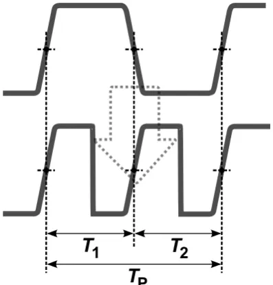
The foregoing Chapter showed that the reference buffer only already accounts for the bigger part of the noise contributions. This leaves little headroom for the rest circuit. Therefore it might be more efficient to only have this buffer in the signal path and find a means of passing through all (both rising and falling) the edges and combining them in such a way that both falling and rising edges become rising edges. This is illustrated in Fig. 3.2.
T
1
T
2
[image:19.595.172.371.486.694.2]T
P
Figure 3.1: Core idea: Use both edges.
14 CHAPTER 3. FREQUENCY DOUBLING
The incoming reference frequency, fxtal, is in this case considered to be a trapezium shaped wave, with finite rise and fall times, and having periodTP. It is chosen to consider this shape wave for sake of simplicity, but this can be any type of waveform as long as the edges are well defined. The analysis for any type of waveform is the same. The period time,TP is considered as being fixed and stable (with the exception of random noise on the edges). Time intervals T1 and T2 are ideally half-periods of TP. In practise these two time intervals depend on the timing of the falling edge in between the two rising edges. By taking advantage of the fact that most clocking circuits are edge sensitive and only ”look” at the rising edges, (which makes the falling edges non-critical), it is possible to turn the falling edges of the reference clock into rising edges and combine them with the already present rising edges. This also means that the then present falling edges are non-critical. The created clock signal now has periods equal to half the period of the reference clock, that isT1andT2, hence
doubled in frequency.
It is worth mentioning that this has an advantage compared to a PLL solution. It is important to notice that with a PLL the doubled frequency is generated by a relatively noisy VCO, which is than ”cleaned up” by the PLL-loop using the crystal rising edges. The Dual-Edge method however has the advantage that it uses the intrinsic clean edges of the reference crystal directly as rising edges for the doubled frequency.
3.1.1
Drawback
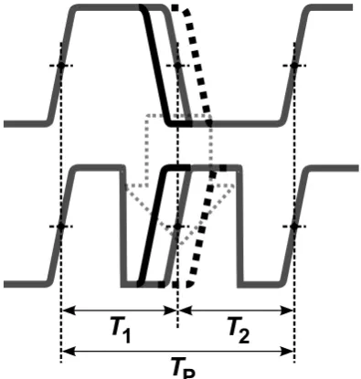
Major drawback of this approach is the timing of the falling edge of the refer-ence clock. When this timing is not exactly at half of the period time,TP, it creates an timing error T1-T2 between adjacent periods of the doubled clock frequency. (Fig. 3.2).
T
1
T
2
[image:20.595.223.421.486.694.2]T
P
3.1. IDEA 15
As can be seen, the error originates at the reference clock that has unequal half-period times, which is most commonly referred to as duty-cycle error. A duty-cycle of 50% means that the ”on” time is 50% of the total period, which makes the adjacent periods equal. A duty-cycle error of 1% means that the duty-cycle is either 49% or 51%, giving unequal adjacent periods. Since the inequality between adjacent periods gives a timing error, it can also be described as a form of jitter. In the following parts of this document the timing error is going to be referred as adjacent period jitter, and is defined as
∆T =T1−T2 (3.1)
The adjacent period jitter that emerges is a recurring phenomenon, that recurs with every period time, TP, of the reference clock frequency. After all, only the falling edge gives a static timing error, whereas the rising edges relative to each other are fixed with period TP. This adjacent period jitter can therefore be considered as deterministic jitter. How this error emerges in the frequency domain can be understood by considering the doubled output frequencyfd being modulated by the reference input frequencyfxtal. Since it is a deterministic phenomenon it emerges as a spurious tone at the distance of fxtalfrom the doubled output frequency fd, in the frequency domain.
3.1.2
Sources of Error
To identify sources of error it is instructive to examine the circuit in Fig.
3.3, a typical crystal oscillator with buffering [8]. The circuit is tuned to the
R1
C1
Rf
C2 Xtal
Vout
Figure 3.3: A Pierce configuration oscillator circuit.
resonance frequency of the crystal, whereω0experiences a total gain of unity
and a phase shift of 180◦. The eventual oscillator signal that is proposed to be used as the reference frequency of the Dual-Edge Doubler, appears at node Vout of the oscillator circuit.
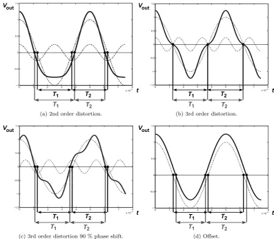
A number a scenarios can be thought of that can introduce time displace-ments of the zero-crossings of the sine wave at node Vout. As shown in Fig.
16 CHAPTER 3. FREQUENCY DOUBLING
Vout
0 1 2 3 4 5 6 7 8
x 10−8
−1 −0.5 0 0.5 1 1.5 t T1 T1 T2 T2
(a) 2nd order distortion.
Vout t T1 T1 T2 T2
0 1 2 3 4 5 6 7 8
x 10−8
−1.5 −1 −0.5 0 0.5 1 1.5
(b) 3rd order distortion.
Vout t T1 T1 T2 T2
0 1 2 3 4 5 6 7 8
x 10−8
−1.5 −1 −0.5 0 0.5 1 1.5
(c) 3rd order distortion 90 % phase shift.
Vout t T1 T1 T2 T2
0 1 2 3 4 5 6 7 8
x 10−8
[image:22.595.148.546.131.477.2]−1 −0.5 0 0.5 1 1.5 (d) Offset.
Figure 3.4: Potential sources of adjacent period timing errors.
distortion causes displacements in the zero-crossings such that the adjacent periods T1 and T2 are not equal anymore. Odd order distortion on the other
hand (Fig. 3.4b and3.4c)does not introduce adjacent period error. That is, it can give zero-crossing displacements, depending on the phase (Fig. 3.4c), but with equal amounts which leavesT1 andT2equal. The signal can also possess
offset, meaning that the dc level can be different than for example an ideal half VDD value. This means that it is not certain on before hand what this level is and has to be anticipated on. Concluding, the sources of error discussed here can all be modelled as adjacent period jitter or duty-cycle error.
3.2
Specifications Revision
3.2. SPECIFICATIONS REVISION 17
quantify numbers in regard to the specifications.
First it is instructive to relate the commonly used duty-cycle error, DCE, to adjacent period jitter, ∆T, as defined above. The duty-cycle error is simply the deviation from its nominal 50% value. Since adjacent period jitter is defined as the difference between the two half-periods, duty-cycle error in relation to adjacent period jitter can be written down as
∆T = 2·DCE fxtal
(3.2) Next an expression for the magnitude of the spurious tone has to be found, to be able to directly relate ∆T to the spurious noise demands in the specifica-tions. The spurious tone emerges at a distance of the reference frequency from the carrier. One can see this as the carrier frequency being phase modulated by the reference frequency. Mathematically a phase modulated carrier can be depicted as [9]
xP M(t) =Accos(ωct+mxB(t)) (3.3) withmbeing called the modulation index and
xB(t) =cos(ωmt). (3.4) How the phase is modulated is illustrated in Fig. 3.5. The bigger the crossing displacement, the bigger the amplitude of the modulation frequency, and hence the bigger the magnitude of the spurious tone. So to know the spurious tone, one simply has to determine the magnitude of the modulation frequency relative to that of the carrier.
The difference between T1 and T2 defines the adjacent period jitter ∆T.
This is related to a peak-to-peak phase difference
∆φpp= ∆T ·π·fout. (3.5) By assuming that the time displacements at the crossing points are caused by the peaks of the excess phase one can state that the peak phase difference
∆φp= ∆φpp
2 , (3.6)
corresponds to two sidebands atfout±fref, each with a relative amplitude in relation to its carrier of
spur= 20·log
∆φ p 2 . (3.7) And hence
spur= 20·log
∆T·π·f
out 4
. (3.8)
3.2.1
Redefinition Of Specifications
18 CHAPTER 3. FREQUENCY DOUBLING
Ideal phase
Excess phase
2π 4π 6π 8π 10π 12π 14π
t1 t2 t3
T2
T1
[image:24.595.154.489.86.372.2]App
Figure 3.5: Phase modulation.
Output Frequency [MHz] Spur [dBc] Adjacent period Jitter [ps] Duty-Cycle Error [%]
40 -47 140 0.15
60 -33 475 0.7
80 -24 1000 2
100 -16 2000 5
Table 3.1: Spur related to jitter and duty-cycle error.
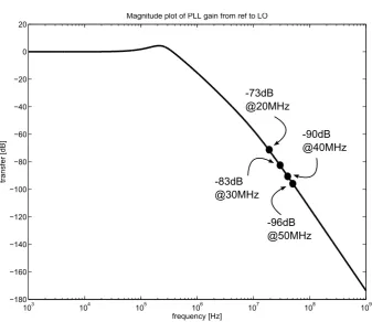
What not yet is done is to include the transfer from the subsequent stage, the frequency synthesizer. It is already stated that this frequency synthesizer has a loop bandwidth of roughly 200 kHz. This means that the spurious tones would fall outside its bandwidth and significantly suppress them. The transfer reaches a roll-off of eventually 40 dB/dec which indicates that the demands get less stringent for a higher doubler output frequencies. The transfer is given in Fig. 3.6.
From this transfer the suppression can be read for the spread of 20 - 50 MHz doubler input frequency. These will be the offset frequencies for the spurious tones relative to the carrier. It is desired to have the spurious tones suppressed as far as -80 dBc at the synthesizer output. Including the step-up ratios 1,
20·logfout
fin
, from the doubler output frequency to the frequency synthesizer output frequency. Table 3.1 shows the revised spur, and when using eq. 3.8
and eq. 3.2, adjacent period jitter and duty-cycle-error demands.
1Step-up-ratio represents the ratio at which the given noise relative to the carrier will
3.3. FREQUENCY DOUBLER IMPLEMENTATION 19
103 104 105 106 107 108 109
−180 −160 −140 −120 −100 −80 −60 −40 −20 0 20
frequency [Hz]
transfer [dB]
Magnitude plot of PLL gain from ref to LO
-73dB @20MHz
-90dB @40MHz
-83dB @30MHz
[image:25.595.103.441.113.405.2]-96dB @50MHz
Figure 3.6: Frequency Synthesizer magnitude plot.
3.3
Frequency Doubler Implementation
A means of realizing a Dual-Edge Doubler implementation, as described in the foregoing sections, is to make use of the properties of a differential amplifier. A differential pair typically amplifies the difference between the two input signals, with the properties of having common-mode rejection, high rejection of supply noise, and high output swings (compared to single-ended). The differential signal processing can be exploited when using a differential pair as doubler circuit.
First, a basic differential pair is shown in Fig. 3.7. The symmetric circuit and isolation from ground through a tail current,It, makes sure that common-mode levels have minimal influence on the bias currents through the transistors, and have therefore common-mode rejection.
Since its basic functionality is to amplify the difference between two signals, the circuit can also be fed by a sinusoid at one side, and its common-mode level at the other side. When their differential polarity is switched around every time at a non-critical moment between the rising and the falling edges of the sinusoid, one obtains the functionality the rising and falling edges are combined into both rising edges. The functionality is shown in Fig. 3.8a.
20 CHAPTER 3. FREQUENCY DOUBLING
RD RD
M1 M2
[image:26.595.228.416.120.294.2]It
Figure 3.7: Basic differential pair circuit.
the edges relative to each other are flipped, giving every edge the same polarity (since they had opposite polarity).
3.3.1
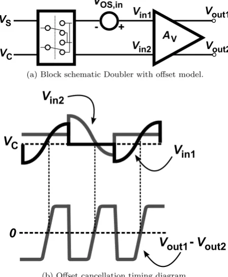
Offset Cancellation
A nice property of this doubler implementation is that the circuit behavior is affected by offsets. Offsets originate from component mismatch in fabrication spreads, by which the symmetry in the circuit is not completely preserved. Components in the left branch, such as resistor, transistor width, or transistor threshold, will not have exactly the same values as the their neighbor compo-nents in the right branch. This constitutes a a-symmetry in the circuit, which creates an input-referred offset at the input. What is interesting to look at is the influence of offset on adjacent period jitter in the circuit as shown in Fig.
3.8a. As stated before, the common mode levels of the two input signals have to be such that the zero-crossings of the output signal are equal. This typically means that the common-mode level of the sinusoid and the reference signal have to be equal. Only then, no extra adjacent period jitter is introduced.
Now consider an offset modelled as an input-referred offset source modelled between the switches and the amplifier input, VOS,in, as shown in Fig. 3.9a. The effect that this offset has on the waveforms2at the inputs,V
in1 andVin2,
is shown in Fig. 3.9b.
From the waveform it can be seen that the effect of offset on adjacent period jitter actually cancels out. Because polarity of the signal is changed every period, both input signals undergo the same offset voltage, and have opposite effects. A certain offset value now creates a positive time shift on one edge, and the same positive time shift on the next edge as well.
2Note that, the effective frequency doubling is actually realized by the switches. The
3.4. ERROR DETECTION 21
RD RD
M1 M2
It
clk
clk
clk
clk
Vout1 Vout2
VS
VC VS
VC
Vin1 Vin2
(a) Differential pair as doubler circuit.
V
out1-
V
out2V
in2-
V
in1V
in1V
in20
V
CV
C [image:27.595.111.434.114.539.2](b) Timing diagram doubler circuit.
Figure 3.8: Differential pair doubler concept.
3.4
Error Detection
As discussed before, any circuit that realizes frequency doubling by combining the rising and falling edges of the input reference clock, is sensitive to the timing of these edges. The foregoing section discussed the doubler circuit with sinusoid waveform as input. This can also be another type of waveform, as long as the signal has clear edge transitions. In case of a sinusoid waveform as input, the edge transitions undergo time displacements for even order distortions in the sinusoid (not for odd order distortions). In case of a square waveform, a source of timing errors is duty-cycle error.
22 CHAPTER 3. FREQUENCY DOUBLING
Vin2 AV
+
Vin1 Vout1
Vout2
-VC
VS
VOS,in
(a) Block schematic Doubler with offset model.
V
in2V
in1V
out1-
V
out20
V
C [image:28.595.209.434.128.402.2](b) Offset cancellation timing diagram.
Figure 3.9: Offset cancellation.
situation (doubler output frequency of 40 MHz), the adjacent period jitter should not exceed 140 ps. When the input is a sinusoid waveform, this comes down to approximately 45 dB 2nd order distortion. For a square waveform its duty-cycle error should not exceed 0.15 %. For both input waveforms this is quite demanding, and not realistic to put on typical crystal oscillator circuitry. Therefore there is the need to reduce the error at the output of the doubler circuit by means of a detection and correction circuit.
A means of achieving this is to measure the two time periods, T1 and
T2, who’s difference defines the adjacent period jitter. To be able to make a
distinction between the two time periods, the waveform is divided such that time periodT1 represents an ’on’ state and time periodT2 represents an ’off’
state. The latter functionality can be implemented by means of a divider circuit.
Since the difference between the two time periods is the error of interest, there has to be a way to compare them. This points to the need of a memory element which stores the time information ofT1and compares it with the time
information ofT2. A straightforward approach is to charge a capacitor during
time period T1 and discharge it during time period T2. This is illustrated in
Fig. 3.10.
3.4. ERROR DETECTION 23
T
1T
2 ΔVerr = 1 C ΔT IiT
pV(t=t1) = 1 C T1Ii V(t=t2) = 1
C T2Ii V1 -
Figure 3.10: Measuring and comparing T1andT2
M
1M
2I
iM
3M
4C
iV
in+V
in-Figure 3.11: Detection circuit
instead of two current sources and/or two capacitors. In this way no mismatch between two of the same components can arise, which minimizes offsets.
The basic operation is to charge and discharge capacitor Ci, during T1,
respectivelyT2(Fig. 3.10). During time periodT1, transistorsM1andM4are
turned on, whereasM2 andM3 are turned off. This creates a positive voltage
across capacitor Ci. During time period T2 the process is turned around, at
which the charge build up is negative. After time periodT2, a rest voltage is
present across capacitorCirepresenting the time difference betweenT1andT2.
The above can however also be used as a continues-time switching integrator when using the signal continuously. From simulations it appeared that the circuit in Fig. 3.11does not act as a pure integrator. Capacitor Ci together with an equivalent ressitance exhibit a time constantCiReq (Fig. 3.12). After settling what is left is a differential signal of the square wave having its DC component linear to the average value of the square wave. Hence, the DC component is linear to the adjacent period jitter, ∆T. When making use of Eq. 3.2, the DC relation between ∆V and ∆T can simply be expressed as
24 CHAPTER 3. FREQUENCY DOUBLING
Req
Ii
[image:30.595.264.382.123.262.2]Ci
Figure 3.12: equivalent circuit.
And its frequency dependant behavior as ∆V = ∆T·fxtal·Req·Ii
sReqCi+ 1
. (3.10)
3.5
Error Correction
Now that the error time signal is detected and available as an error voltage, there has to be a means to use this and correct the input signal. As already briefly mentioned before in the pre-system model there has to be a substrac-tion/addition point somewhere to close the loop. Furthermore, since the output of the detector is a differential signal, there also has to be a way of combining this successfully with the single-ended reference voltage for the doubler [Fig.
3.13].
+
-+
-{
VC
Detector diff. output signal Vref
[image:30.595.261.382.486.593.2]3.6. COMPLETE CIRCUIT FUNCTIONALITY AND SIMULATIONS 25
This reference voltage for the doubler circuit is chosen to be halfVDD, since this is a good approximation of the DC/common-mode level of the reference clock. A switched capacitor circuit that combines the reference voltage out of VDD with the differential output signal of the detector into one single ended signal suitable as corrected reference signal for the doubler circuit is shown in Fig. 3.14. The high glitches from the sampling action can, if necessary, be filtered out by a low-pass filter.
CS1 CH1
{
De
tec
tor
d
iff
.
ou
tpu
t s
ig
na
l
CS2 CH2
VDD
[image:31.595.203.340.221.368.2]VC
Figure 3.14: Correction circuit.
3.6
Complete Circuit Functionality and Simulations
To be able to give a good overview of how the discussed circuit design looks like, the complete circuit schematic is given in Fig. 3.15. As can be seen, all the sub-circuits as discussed in this Chapter are present, which include: doubler, divider, detector, corrector.
The doubler circuit at this point also includes a second stage. This second stage purely amplifies the signal from the first stage, thus making its edges steeper. This can have a positive effect on the noise transfer since steeper edges produce less jitter. Next to that, it also has the functionality to convert the differential signal from the first stage to a single ended signal. This is done because the signal from the second stage has to drive the divider which is implemented as a single ended Flip-Flop.
26 CHAPTER 3. FREQUENCY DOUBLING
clk
clk clk
clk
D clk Q Q
VDD
DIVIDER
ΔT DETECTOR DOUBLER
CORRECTOR VC
Vout
(a) Time discrete feedback.
clk
clk clk
clk
D clk Q
Q
DIVIDER
ΔT DETECTOR DOUBLER
VC
Vout
+
[image:32.595.151.540.87.726.2]-(b) Time continues feedback.
3.7. SUMMARY 27
3 3.5 4 4.5 5
x 10−6
0.5 0.52 0.54 0.56 0.58 0.6 0.62 0.64 0.66 0.68 0.7
Time [sec]
Control Voltage Vc [V]
Circuit Simulations
[image:33.595.129.464.111.420.2]Reference frequency: 20MHz Reference frequency: 50MHz
Figure 3.16: Simulation results for input frequencies of 20 and 50 MHz.
3.7
Summary
Chapter 4
System Analysis
The foregoing chapter described the electrical circuit and implementations in sub-parts. Now that it is clear how the system on circuit level can be imple-mented, it would be good to have a detailed system analysis. It is firstly desired to gain insight in how the systems transfer function look like. And secondly to be able to predict the system responses to several parameter values. The analysis is based on the circuit as shown in3.15b of the previous chapter. A low-pass filter is included in the analysis since this was part of the original circuit design. A low-pass filter is still optional to filter out the high-frequency components from the correction circuit as discussed in Chapter3.
First, a more detailed system model is given in Fig. 4.1. In this system model every sub-circuit as discussed in the foregoing chapter can be found along with their signals quantities and units.
+
-+
-VC
Vref
Doubler
Divider
LPF DetectorΔT
+
ΔVin
[V]
[V]
ΔVout
[V]
ΔTout
[sec]
[V] [V] [sec]
Vi Tdi
Figure 4.1: Detailed system model.
The input parameter, ∆Vin, is the deviation voltage around the reference voltage,Vref, and is not a physical node voltage. Together with the crystal ref-erence frequency it controls the adjacent period jitter, and can thus be seen as the parameter to which the system responds. This makes the crystal reference frequency, in the sense of the control loop, merely an external parameter of the doubler sub-block. This thought can be clarified by considering the timing sketch in Fig. 4.2.
30 CHAPTER 4. SYSTEM ANALYSIS
T
1T
1T
2T
2ΔT
outΔV
inA
pp [image:36.595.209.436.120.321.2]t
1t
nt
2Figure 4.2: relation ∆Vin and ∆Tout
As indicated before, ideally the reference voltage,Vref, has exactly the same value as the DC voltage level coming from the crystal reference frequency. This gives minimal adjacent period jitter, assuming that the input sine has no 2nd order distortion. One reason to model the problem like this is that the detector circuit detects the timing error and transfers it to a voltage error, hence the feedback signal has the unit voltage and needs to be compared to a signal with the same unit. And secondly, this is a way to define the problem because every form of adjacent period jitter can be related to a voltage difference, ∆Vin. The latter relation can be described when considering the zero-crossing timing labels, t1, tn (nominal), and t2, from Fig. 4.2. Then, from definition it is
known that
∆T =T1−T2. (4.1)
Where
T2=t2−tn (4.2)
and
T1=tn−t1. (4.3)
Substitution gives
∆T = 2tn−t1−t2. (4.4)
Considering that a voltage deviation, ∆Vin, gives a small time deviation,δt on every edge. It can be seen in Fig. 4.2that this deviation gives a right shift on the first edge, a left shift on the second edge, and again a right shift on the third edge. In algebraic terms:
∆T = 2(tn−δt)−(t1+δt)−(t2+δt). (4.5)
4.1. LINEARIZED SYSTEM MODEL 31
This means that the difference betweent1andt2is always the same, namely
the period time. Therefore, the adjacent period jitter ∆T is a measure that shifts within the fixed time frame of the period time.
∆T = 4δt. (4.7)
Where
δt= ∆Vin
SlewRate. (4.8)
And so
∆T = 4∆Vin
SlewRate. (4.9)
4.1
Linearized System Model
In order to quantify the behavior of this circuit design’s system model, it is essential to approximate a linearized model of the system. To do so, the system can be linearized around the nominal time TN, which is essentially shown in the derivations as shown in the last section.Since adjacent period jitter is the measure of interest every sub-circuit can be considered as linearized within this deviation regime. When following this, the system model from Fig. 4.1can be re-stated as shown in Fig. 4.3. For sake of completeness it is chosen to have as
VC
Vref
+
ΔVin ΔTout
-4SR
DC
+
+
R 1fCf
s + 1
I R f RiCi si i + 1xtal 4
SR
ΔTin
Figure 4.3: Linearized system model.
input quantity ∆Tin which coincides with ∆Tout as an output quantity. This gives a better overview, since a certain ∆Tinat the input has to be reduced to a minimum value for ∆Tout at the output, although the essential control loop is from ∆Vin to ∆Vout.
The transfer of the doubler sub-circuit is merely the relation from Eq. 4.9. Again it is important to state that the actual doubling work is done by the flipping actions as carried out by the switches, where the amplifier merely amplifies the signal after it is doubled. This means that the slew rate of the incoming crystal signal is the parameter in the transfer. Another important aspect is that an ideal divider is transparent to every rising edge that it is being fed. Essentially a divider toggles at every rising edge. Therefore the divider can be seen as a sub-circuit that merely makes a waveform translation, suitable for the detector to work with, and can be left out of the equations1.
The detector itself has the transfer function which has been described by Eq.
1As already stated this counts for an ideal situation. In practise the divider has influence
32 CHAPTER 4. SYSTEM ANALYSIS
3.10 in Chapter 3. This together with the transfer function of the low pass filter makes a loop transfer of the 2nd order, whereas the open loop transfer is expressed as
H(s)|open= ∆Vout
∆Vin
(s)|open (4.10)
H(s)|open= 4 SR ·
IiRifxtal sRiCi+ 1
· 1
sRfCf+ 1
. (4.11)
Or in a different form
H(s)|open= 4 SR ·
Iifxtal sCi+R1i
· s 1
ωLP F + 1
, (4.12)
which shows that the pole due to the low pass filter is fixed. The second pole introduced in the detector’s integrator is more or less a dynamic parameter because of its dependence on the equivalent resistance in the circuit. This also reveals that the open loop gain will not go to infinity for frequencies approaching zero, which indicates that the closed loop step response will exhibit a steady-state error. The closed loop has a unity feedback which makes its transfer
H(s)|closed=
4
SRIifxtal ( s
ωLP F + 1)(sCi+ 1
Ri) + 4
SRIiftal
. (4.13)
4.1.1
Behavioral quantification
Eq. 4.13suggests due to its second-order transfer function, that the step re-sponse of the system can be overdamped, critically damped, or underdamped. It would be helpful in designing the system to be able to derive conditions for these cases. To do so, it is convenient to rewrite in a more familiar form as used in control theory,
H(s)|closed=
ω2
n s2+ 2ζω
ns+ωn2
, (4.14)
with ωn and ζ being the systems resonance frequency and damping factor respectively.
Rewriting Eq. 4.13in the form of Eq. 4.14gives
H(s)|closed=
4
SRIiftal
RfCfCi
s2+s( 1
RiCi + 1
RfCf) + 1
RiCiRfCf +
4
SRIiftal
RfCfCi
. (4.15)
Comparing this to the standard form leads to a relation for the system’s reso-nance frequency,
ωn=
s
1 RiCiRfCf
+
4
SRIiftal RfCfCi
, (4.16)
and for the system’s damping frequency,
ζ=
1
RiCi + 1
RfCf
2q 1
RiCiRfCf +
4
SRIiftal
RfCfCi
4.1. LINEARIZED SYSTEM MODEL 33
As mentioned before the system exhibits a steady-state error due to impu-rity of the detector’s integrator circuit. An important issue because this error is not allowed to exceed the minimum allowable error as stated in the speci-fications section. It is relevant to also be able to quantify this error seen its importance.
Before any approximation can be made, it is important to first derive a basic expression for the error signal for system in Fig. 4.3. Again, because of unity feedback, the error is
VC= ∆Vin−∆Vout= ∆Vin−H(s)|openVC (4.18) which can be expressed in terms ofVC only as
VC=
∆Vin 1 +H(s)|open
. (4.19)
Now the steady-state error can be approximated by making use the final-value theorem
lim
t→∞vc(t) = lims→0ysVC(s) (4.20) lim
t→∞vc(t) = lims→0
s∆Vin(s) 1 +H(s)|open
. (4.21)
Where ∆Vinis a unit step input, and so ∆Vin(s) =
1
s. (4.22)
The steady-state error of the closed-loop system then becomes ess(t) = lim
s→0
1 1 +H(s)|open
. (4.23)
4.1.2
Time Discrete Feedback
The circuit as described in Fig. 3.15a of Chapter 4 has a different transfer model as the system that has been described until now which is based on the circuit in Fig. 3.15bof Chapter 4. The correction circuit in Fig. 3.15amakes use of sample-and-hold which involves a dead-time. Fig. 4.4shows the system model, where the LPF is replaced by the dead-time transfer.
VC
Vref
+
ΔVin ΔTout
-4SR
DC
+
+
s I R fRiCi si i + 1xtal 4
SR
ΔTin
[image:39.595.102.487.597.696.2]e
-1/4T34 CHAPTER 4. SYSTEM ANALYSIS
The open-loop transfer is
H(s)|open= 4 SR ·
IiRifxtal sRiCi+ 1
·e−14T s. (4.24)
The closed loop transfer function can best be written in the Z-domain to be able to approximate the dead-time. This is done by using the forward-euler approximation which can be solved using Matlab. This is nothing more than a transformation of the transfer model as described in the foregoing section.
4.2
Simulation comparison
The system analysis along with its behaviorial quantification allows to design the circuit such that it behaves according to things such as settling time, over-shoot and steady-state error. The model as described predicts the circuits behavior, so it is a first necessity to examine if the predictions of the system model match circuit simulations.
4.2.1
Time Continuous Model
Fig. 4.7 shows two step response plots in which the system model predic-tions are compared with the circuit simulapredic-tions2 based on the circuit in Fig. 3.15b of Chapter 4. For the step response in Fig. 4.5a an input frequency of 20MHz is used with the following circuit component values: Ii = 100µA, Ci = 50pF, Rf = 100kohm, and Cf = 5pF. For these values the step re-sponse of the approximated system model that predicts a resonance frequency ωn of approximately 2.9E6rad/sec and a damping of approximately 0.34. The same goes for Fig. 4.5b, where the circuit component values are: Ii= 100µA, Ci = 5pF, Rf = 100kohm, and Cf = 10pF. This gives a resonance frequency ωn of approximately 6.3E6rad/sec and a damping of approximately 0.08. Both simulations show good accordance with predictions of the system model, apart from a small static offset error in the circuit simulations. The latter can be subscribed to small offsets in the detector circuit that occur when the driven signal has unequal rise and fall times. The error however is in the range of 50 ps, which is still far beyond the minimum specification of 140 ps for this input frequency.
For the simulation results as shown in Fig. 4.7 the value of Ri that is the equivalent resistance in the detector circuit, could be still neglected. This can also be understood from Eq. 4.17, that shows that if the part 1/RiCi is relatively small compared to 1/RfCf,Ridoes not play a significant role in the damping of the system. This changes however for different circuit component values and different W/L values for the transistors in the detector circuit. The simulation results that are shown in Fig. 4.6 give two different circuit simulations with their system model predictions. For both simulations the component values are: Ii= 10µA,Ci= 1pF,Rf = 100kohm, andCf = 50pF. One simulation is carried out with a W/L of the transistors of 1.6 and gives a fairly small damping ratio of 0.05. For this case Ri is not accounted for in the system model and gives a reasonable prediction. For the other simulation
2Note that the horizontal axis of the plots are in units of cycles. One cycle equals the
4.2. SIMULATION COMPARISON 35
400 450 500 550 600 650 700 750 800
−4 −2 0 2 4 6 8 10
12x 10
−10
Cycles
Adjacent Period Jitter [sec]
System Model vs. Circuit Simulation
System Model Circuit Simulation
(a) Resonance frequency and damping of approximately 460kHzand 0.34 respectively.
400 450 500 550 600 650 700 750 800
−1 −0.8 −0.6 −0.4 −0.2 0 0.2 0.4 0.6 0.8 1
x 10−9
Cycles
Adjacent Period Jitter [sec]
System Model vs. Circuit Simulation
System Model Circuit Simulation
[image:41.595.129.468.465.753.2](b) Resonance frequency and damping of approximately 1M Hzand 0.08 respectively.
36 CHAPTER 4. SYSTEM ANALYSIS
400 450 500 550 600 650 700 750 800
−1 −0.8 −0.6 −0.4 −0.2 0 0.2 0.4 0.6 0.8 1
x 10−9
Cycles
Adjacent Period Jitter [sec]
System Model vs. Circuit Simulation (Different W/L)
[image:42.595.181.516.132.419.2]System Model: Ri=inf System Model: Ri=1.25Mohm Circuit Simulation: W/L=17 Circuit Simulation: W/L=1.7
Figure 4.6: Simulation results for different W/L values.
a W/L of 16 is taken which shows a significant change in damping ratio. Now Ri has to be taken in account for the system model to match up, which then gives a damping of 0.24. These results indicate that for higher W/L ratios, the off-resistances cannot be neglected and have to be taken in account to make an accurate prediction.
4.2.2
Time Discrete Model
The following simulation results are based on the circuit as shown in Fig. 3.15a
4.2. SIMULATION COMPARISON 37
1200 130 140 150 160 170 180 190 200
0.2 0.4 0.6 0.8 1
1.2x 10
−8
Cycles
Adjacent Period Jitter [sec]
System Simulation vs. Circuit Simulations
Cicuit Simulation System Model
(a)
120 130 140 150 160 170 180 190 200
−2 0 2 4 6 8 10
12x 10
−9
Cycles
Adjacent Period Jitter [sec]
System Simulation vs. Circuit Simulations
Cicuit Simulation System Model
[image:43.595.133.467.138.772.2](b)
38 CHAPTER 4. SYSTEM ANALYSIS
4.3
Summary
Chapter 5
Noise Estimation
One of the motivations to choose for the side-track of the Dual-Edge approach was that a PLL solution showed difficulties in meeting the phase noise demands. This Chapter will estimate the noise performance of the Dual-Edge Doubler by identifying and quantifying noise contributions. This will be supported with simulation results. Before doing so, a short introduction in the theory behind the noise estimation for circuits with a sampled nature will follow. The ’Spectr-eRF’ documentation is not always very clear about the mathematical definition of the output quantities produced by PSS analysis. The most useful informa-tion that can be found mainly comes from the website designerguide.com [10], [11], [12].
5.1
Noise in Sampled Systems
The doubled frequency as generated by the proposed Dual-Edge method is used as an edge-sensitive clock for the next stage. The next stage is triggered by the rising edge, which is also the reason why only this edge deserves further attention. More specifically it can be considered that the next stage is triggered by the output rising edge of the Doubler when it crosses a certain threshold valueVth. For CMOS gates this is usually around half the supply voltage. This is illustrated in Fig. 5.1.
V
outV
th [image:45.595.177.365.563.683.2]T
outt
Figure 5.1: Waveform of Doubler output.
40 CHAPTER 5. NOISE ESTIMATION
5.1.1
Cyclostationary Noise
It may be clear that the noise of interest is the noise that is present on the rising edge, and more specifically at threshold moment Vth. Because of the noise present at this threshold moment, it triggers the next stage at some time instant different from the ideal. To understand the noise behaviour, the notion of cyclostationary noise is useful.
The name cyclostationary noise refers to the fact that it is cyclic or periodic stationary1 noise. It is generated by circuits whose operating points change
periodically in time. The time-varying operating point modulates the output noise of noise sources whose output noise depends on a operating point (one can think of it as a voltage controlled noise source). Cysclostationary noise occurs in every non-linear circuit that is driven by a large periodic signal, which are for example inverters, dividers, and the Dual-Edge circuit as proposed in this Thesis. To clarify the above, the cyclostationary nature of the noise at the the output of the Doubler is illustrated in Fig. 5.2.
V
outV
thT
outt
V
Nout [image:46.595.222.425.324.561.2]t
Figure 5.2: Illustration of cyclostationary noise at output of Dual-Edge Doubler circuit.
5.1.2
Noise Sampling
To be able to see the cyclostationary noise, one has to obtain a instantaneous Power Spectral Density (PSD)2. An instantaneous PSD is taken by sampling
1Stationary noise is noise whose static properties do not change over time.
2The traditional PSD is referred to as the time-averaged PSD, what is measured by a
5.1. NOISE IN SAMPLED SYSTEMS 41
the noise at the desired threshold moment with the same periodicity as the cyclostationary noise [Fig. 5.3]. This results in a time-discrete noise samples for which the PSD can then be computed. This can be produced by ’SpectreRF’ by using the strobed pnoise function.
Vout
Vth
Tout
t
VNout
t
Nout,i
[image:47.595.167.376.188.413.2]t
Figure 5.3: Sampling of noise at threshold moments (lower graph is magnified).
Since the stationary noise is modulated by a periodic signal, the noise will manifest itself around the fundamental of the periodic signal and the harmonics it produces. This together with the sampled nature of the noise process makes that all the noise contributions fold back into one band whose spectrum is periodic in fs (which is equal to the modulation frequency). This is clarified in the illustration of Fig.5.4.
s
f
f
S (f)
s
f
2
Φ
Figure 5.4: Folding of the noise spectrum.
[image:47.595.148.398.535.666.2]42 CHAPTER 5. NOISE ESTIMATION
noise folding components. How many sidebands this should be depends on the effective bandwidth of the circuit.
5.2
Noise and Jitter
In clock circuits it is more desirable to express noise in terms of jitter. Jitter is the time domain equivalent of phase noise in the frequency domain. The directly observed noise on an edge at a certain crossing momentVth causes a time displacement of the crossing moment (jitter) whose magnitude depends on the steepness of the edge. Therefore, noise in the voltage domain is related to jitter in the time domain by the time derivative of the edge or slew rate (SR)[Fig. 5.5]. This means that a steeper edge converts less noise from the
Δv
Δt
t
t
ihistogram
n
jitter
hi
st
ogr
am
noise
v
thv
n
Δv
n( )
t
iSR( )
t
i [image:48.595.163.482.299.503.2]Δt ( ) =
t
iFigure 5.5: Relation of noise in the voltage and jitter in the time domain.
voltage domain to jitter in the time domain.
5.2.1
Definitions
There are different kinds of definitions of how to describe and quantify noise. This subsection is meant to define what kind of relations and definitions the author of this Thesis uses to estimate the noise in the next sections.
The most common measure is the power spectral density of the voltage,Sv. This is what is usually directly observed by a spectrum analyzer and the most common measure in simulators such as ’SpectreRF’3. When talking in terms
of phase noise, Sφ is used, which is the power spectral density of the phase.
3This is because traditional noise analysis in circuit simulators derived from SPICE is
5.3. NOISE ESTIMATION AND SIMULATIONS 43
A third measure isL, which is the power spectral density of the voltage,Sv, normalized to its carrier.
To relate this to the sampled cyclostationary noise of interest, SpectreRF producesSvi(f). This is the spectral density of the random time-discrete noise
using the process as described in Paragraph 5.1. According to [12] this is related the the spectral density of the phase by
L(f) = 2·
πf
out SR
2
·Svi(f). (5.1)
To the best of the authors knowledge, the spectral density definitions as used by SpectreRF are single-sided representations.
For jitter, the definition absolute jitter4 is used. The variance of absolute
jitter is related to the total area of the power spectrum of the phase5[13]
σA2 = 1 2(πfout)2
Z fout 0
L(f)df. (5.2)
Now it is possible to calculate the jitter from the spectral density Svi(f)
that SpectreRF produces, by combining5.1and5.2, which yields
σA2 = 1 SR2
Z fout 0
L(f)df. (5.3)
5.3
Noise Estimation and Simulations
To come to a noise estimation, first the most dominant noise sources have to be identified. Fig. 5.6shows the Dual-Edge Doubler system model including the control loop as discussed in Chapter4. As indicated, the dominant noise sources to be expected are the amplifier after the doubling switches, the sample and hold circuit and the ∆T Detector.
-amplifier
Divider
S&H ΔT
Detector
+
Doubling outswitches
Doubler Unit
in
[image:49.595.103.476.495.605.2]f
Figure 5.6: System model indicating dominant noise sources.
The reason for the amplifier to be expected as a dominant noise source is because it essentially fulfills the same role as a reference buffer in classical clock-ing circuits. As discussed in Chapter2in the PLL system the reference buffer
4in ’SpectreRF’ this is called edge-to-edge jitter,J2
ee
5Strictly spoken, the variance of absolute jitter is directly related to its own power
44 CHAPTER 5. NOISE ESTIMATION
accounts for 70% of the total noise. A reference buffer as such is still needed to obtain a clock signal with steep edges from a slow sine wave. The sample and hold circuit is expected to account for a significant amount of noise due to the on-resistance in combination with the hold capacitors that givekT /Cnoise. First an estimation of the noise sources that are assumed white are given. These sources include the thermal noise from (Fig. 5.7):
• Drain resistors of the differential pair.
• Transistors of the differential pair.
• Transistors of second amplifier stage.
• Current mirror load of second amplifier stage
• Tail current source of integrator.
• On-resistors in sample-and-hold circuit (kT/C noise).
clk
clk clk
clk
D clk Q Q
VDD VC
Vout
Drain resistor noise
Transistor noise 1st stage
Transistor noise 2nd stage
Current-mirror noise
Tail current noise kT/C
[image:50.595.151.540.349.623.2]noise
Figure 5.7: Circuit overview indicating dominant noise sources.
5.3. NOISE ESTIMATION AND SIMULATIONS 45
parameters 1st amp. stage 2nd amp. stage integrator sample-and-hold
Rd[ohm] 600 11k
ro[ohm] 850 8.5k
gm[ohm−1] 12m 800µ 620µ
Itail[A] 1m 100µ 100µ
Ci[F] 50p
Ch[F] 10p
[image:51.595.103.443.124.207.2]Noise Bandwidth [Hz] 1G 3G
Table 5.1: Parameter values first test design.
Drain resistor noise
The noise contributions of both drain resistors in the first amplifier stage can be estimated by knowing there spectral densities. The one-sided PSD of a resistor is
I2
n,Rd= 4kT /Rd. (5.4)
The total noise power contributed by the drain resistor to the output nodeVout can be stated asV2
out,Rd= 4kT /Rd·(Rd//ro)
2·Av2
2·fN B. WhereAv2is the gain
of the second amplifier stage andfN B is the bandwidth of the noise. For the drain resistor vale as shown in Table5.1the total noise power at the output of the buffer stage is approximatelyV2
out,Rd= 4kT /600·(600//850)
2·42·1×109≈
5×10⁻⁸V2/Hz. This can be converted to jitter by dividing the latter number
by the slew rate at nodeVout. The total jitter isτrms2 = 4e−8/(630×106)2≈ 1.25×10⁻²⁵sec2. The noise to carrier ratioLcan be found using the following
relation (where5.2is used)
L= 2π2foutτrms2 . (5.5) Finally, the two drain resistors in th
![Figure 2.7: ISSCC low-jitter PLL designs with FoM [4].](https://thumb-us.123doks.com/thumbv2/123dok_us/1210588.644689/16.595.165.471.106.350/figure-isscc-low-jitter-pll-designs-fom.webp)