ISSN (Print) : 2320 – 3765 ISSN (Online): 2278 – 8875
I
nternational
J
ournal of
A
dvanced
R
esearch in
E
lectrical,
E
lectronics and
I
nstrumentation
E
ngineering
(A High Impact Factor, Monthly, Peer Reviewed Journal)
Website: www.ijareeie.com
Vol. 8, Issue 2, February 2019
Controlled Rectifier with Improved Dynamic
Response for Under Unbalanced Supply and
Variable Line and Load Inductances
Ashik K S , Deepan Kishore S , Mohamed Ibrahim K , Rajesh S , K V Bindu
UG Scholar, R.M.K. College of Engineering and Technology, Thiruvallur, Tamil Nadu, India
UG Scholar, R.M.K. College of Engineering and Technology, Thiruvallur, Tamil Nadu, India
UG Scholar, R.M.K. College of Engineering and Technology, Thiruvallur, Tamil Nadu, India
UG Scholar, R.M.K. College of Engineering and Technology, Thiruvallur, Tamil Nadu, India
Assistant Professor, R.M.K. College of Engineering and Technology, Thiruvallur, Tamil Nadu, India
ABSTRACT: To simulate and implementation of controlled rectifier with improved dynamic response for under unbalanced supply and variable line and load inductances. With the widespread use of power electronics devices such as rectifier, inverter etc. in power system causes serious problem relating to power quality. One of such problem is generation of current and voltage harmonics causing distortion of load waveform, voltage fluctuation, voltage dip, heating of equipment etc. Also presence of non-linear loads such as UPS, SMPS, speed drives etc. causes the generation of current harmonics in power system. They draw reactive power components of current from the AC mains, hence causing disturbance in supply current waveform. Thus to avoid the consequences of harmonics we have to compensate the harmonic component in power utility system. To simulate controlled Rectifier with open loop system. To simulate controlled Rectifier with closed loop PI controller system. To simulate controlled Rectifier with closed loop FOPID controller system.
KEYWORDS: Controlled Rectifier, Pulse width modulation (PWM).Total harmonic distortion (THD), Proportional integral (PI), Fractional order Proportional integral derivative (FOPID).
I. INTRODUCTION
ISSN (Print) : 2320 – 3765 ISSN (Online): 2278 – 8875
I
nternational
J
ournal of
A
dvanced
R
esearch in
E
lectrical,
E
lectronics and
I
nstrumentation
E
ngineering
(A High Impact Factor, Monthly, Peer Reviewed Journal)
Website: www.ijareeie.com
Vol. 8, Issue 2, February 2019
Nonlinearity causes generation of harmonics that result in poor power quality, voltage distortion, low power factor at input side, slow varying rippled dc output at load end and low efficiency. Harmonics of input current causes overheating of transformers, power cables and motors, inadvertent tripping of relays, incorrect measurement of voltage and current by meters and increased iron losses in transformers. Harmonics also cause motors to heat up and produce pulsating torque. Buildings with large number of computers and data processing equipment use AC-DC conversion for their supply. AC-DC converters draw harmonic current which cause neutral current. Besides power quality problems at user ends and utility, harmonics also cause problems on other users. . A method to reduce harmonic pollution caused by the three phase rectifiers is the third harmonic current injection. The technique applies injection of third harmonic currents in the rectifier supply lines in order to modify the input current waveform &to reduce its distortion.
Nowadays step-up converters are used in many applications, especially in renewable energy systems such as those based on PV panels and fuel cells. These converters usually require to step-up low voltages in order to meet the nominal requirements of grid-connected inverters. Currently, there exist several topologies with high volt- age conversion ratios, e.g. those that are based on coupled-inductors. For instance, in [1] the authors introduce Y-source boost DC/DC converter whose high voltage gains are enabled via a tightly coupled three-winding inductor. This converter shows in general interesting design and dynamic properties that are suitable for distributed generation applications. In [2], a high voltage gain multi-coupled inductor based topology is introduced; this topology exhibits automatic current balancing and high-power density, with respect to other coupled-inductor based topologies, since its multi-coupled inductor design per- mits to optimize the use of the core material. Other high voltage gain topologies that are based on coupled inductors can be found in [3]–[10].Although such devices represent a very plausible solution at achieving high conversion ratios and overall good performance, they usually require standard (i.e. non-commercial) magnetic components for their design. Moreover,the required size of the overall converter might be also larger than that of topologies that require only small inductors, due to the need of bulky core materials. As an alternative to these configurations, transformer-less topologies can be constructed with devices off-the-shelf, which is a compelling solution that permits to reduce the design process, size and overall cost of the converter. Such transformer-less topologies, can be J.E. Valdez-Resendiz, J.C. Mayo-Maldonado, J. Loranca-Coutio, C.A. Villarreal-Hernandez and G. Escobar-Valderrama are with School of Engineering and Sciences at Tecnologico de Monterrey, Monterrey, Mexico.
J.C. Rosas-Caro is with Academia de Electrica, Electronica y Control at Universidad Panamericana, Zapopan, Mexico. based on several strategies such as: (i) switched-capacitors as voltage multipliers (see [11]–[16]), with linear voltage gains; (ii) electrical configurations that allow the connection of input parallel- and output series- converter stages to improve performance and achieve large gains (see [17]–[20]); (iii) quadratic gain stages (see [21]–[24]), with important features e.g. high gain with a reduced number of switches. Though, e.g. switched capacitor converters have become a popular solution to achieve high-voltage gains, they also have some disadvantages. For instance they exhibit high current spikes due to due to abrupt parallel connections between capacitors leading to to high conduction losses. Moreover, there exist also charging/discharging losses that reduce the efficiency of such converters (cf. [25]).
In this paper, we focus on providing a new solution for the specific challenging need to develop new power converter topologies for renewable energy applications. In particular for those scenarios that demand high voltage gains, low cost implementations and high efficiency. In particular, we propose a novel step-up DC-DC converter with quadratic gains, whose main advantages are (i) simple single-switch structure, (ii) low voltage rated capacitors compared with traditional quadratic boost converters (QBC), (iii) modularity, several switching stages can be easily stacked in order to increase the output voltage gain. The underlying operation principle of the pro- posed converter is validated with experimental results
II. CONTROLLED RECTIFIER WITH IMPROVED DYNAMIC RESPONSE
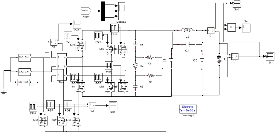
2.1 Circuit-Description
ISSN (Print) : 2320 – 3765 ISSN (Online): 2278 – 8875
I
nternational
J
ournal of
A
dvanced
R
esearch in
E
lectrical,
E
lectronics and
I
nstrumentation
E
ngineering
(A High Impact Factor, Monthly, Peer Reviewed Journal)
Website: www.ijareeie.com
Vol. 8, Issue 2, February 2019
current injection for three phase diode bridge rectifier. Ali M Eltamaly (2012) has introduced a single phase controlled converter in the injection path to control the angle of injection current for each firing angle of a three phase controlled converter. He has also revealed optimal relation between the firing angle of three-phase and single phase controlled converter for minimum THD. Proposed system using closed loop controlled system.
Fig-1. The circuit-diagram of Existing system
Fig-2. The circuit-diagram of Proposed system
III. SYSTEM-DESCRIPTION
ISSN (Print) : 2320 – 3765 ISSN (Online): 2278 – 8875
I
nternational
J
ournal of
A
dvanced
R
esearch in
E
lectrical,
E
lectronics and
I
nstrumentation
E
ngineering
(A High Impact Factor, Monthly, Peer Reviewed Journal)
Website: www.ijareeie.com
Vol. 8, Issue 2, February 2019
Fig.3. Block-Diagram of PI – controlled AC-DC converter system
“Block-Diagram of FOPID – controlled AC-DC controlled rectifier system is shown in Fig.4. ‘Voltage at load ‘is sensed and it is evaluated with the reference-voltage to get Voltage-Error (VE). This ‘VE is directed to a FOPID-controller’. The ‘yield of PI’ is used to adjust the Pulse-Width (PW) of controlled Rectifier.
Fig.4.Block-Diagram of FOPID – controlled AC-DC converter system
IV. RESULTS AND DISCUSSION
ISSN (Print) : 2320 – 3765 ISSN (Online): 2278 – 8875
I
nternational
J
ournal of
A
dvanced
R
esearch in
E
lectrical,
E
lectronics and
I
nstrumentation
E
ngineering
(A High Impact Factor, Monthly, Peer Reviewed Journal)
Website: www.ijareeie.com
Vol. 8, Issue 2, February 2019
Fig.5.Circuit diagram of controlled rectifier with C filter
Fig.6.Input voltage & current
ISSN (Print) : 2320 – 3765 ISSN (Online): 2278 – 8875
I
nternational
J
ournal of
A
dvanced
R
esearch in
E
lectrical,
E
lectronics and
I
nstrumentation
E
ngineering
(A High Impact Factor, Monthly, Peer Reviewed Journal)
Website: www.ijareeie.com
Vol. 8, Issue 2, February 2019
Fig.8.Voltage across RL load
Fig.9.Voltage Ripple
Fig.10. Current Through load
ISSN (Print) : 2320 – 3765 ISSN (Online): 2278 – 8875
I
nternational
J
ournal of
A
dvanced
R
esearch in
E
lectrical,
E
lectronics and
I
nstrumentation
E
ngineering
(A High Impact Factor, Monthly, Peer Reviewed Journal)
Website: www.ijareeie.com
Vol. 8, Issue 2, February 2019
Circuit diagram of controlled rectifier with Cascade filter is delineated in Fig.12. Input voltage & current are delineated in Fig.13 & the values are 260V and 30A respectively. Current THD is delineated in Fig.14 &its value is 23.93%. Voltage across RL load is delineated in Fig.15 &its value is 370V. Voltage Ripple is delineated in Fig.16 &its value is 355.5V. Current Through load is delineated in Fig.17 &its value is 37A. Output power is delineated in Fig.18 &its value is 13000W.
Fig.12.Circuit diagram of controlled rectifier with Cascade filter
Fig.13.Input voltage and current
ISSN (Print) : 2320 – 3765 ISSN (Online): 2278 – 8875
I
nternational
J
ournal of
A
dvanced
R
esearch in
E
lectrical,
E
lectronics and
I
nstrumentation
E
ngineering
(A High Impact Factor, Monthly, Peer Reviewed Journal)
Website: www.ijareeie.com
Vol. 8, Issue 2, February 2019
Fig.15.Voltage across RL-load
Fig.16.Voltage ripple
Fig.17.Current through load
Fig.18.Output power
ISSN (Print) : 2320 – 3765 ISSN (Online): 2278 – 8875
I
nternational
J
ournal of
A
dvanced
R
esearch in
E
lectrical,
E
lectronics and
I
nstrumentation
E
ngineering
(A High Impact Factor, Monthly, Peer Reviewed Journal)
Website: www.ijareeie.com
Vol. 8, Issue 2, February 2019
Table 1
Comparison of voltage ripple, current THD
Controlled rectifier Vor Current THD
C-Filter 3.0V 42.01%
Cascade -Filter 0.6V 23.93%
Circuit diagram of controlled rectifier in open loop with disturbance is delineated in Fig.19. Input voltage is delineated in Fig.20. &its value is 420V. Output voltage across RL load is delineated in Fig.21 &its value is 490V. Output current through load is delineated in Fig.22 &its value is 44A. Output power is delineated in Fig.23 &its value is 2.2*104W.
Fig.19.Circuit diagram of controlled rectifier in open loop with disturbance
ISSN (Print) : 2320 – 3765 ISSN (Online): 2278 – 8875
I
nternational
J
ournal of
A
dvanced
R
esearch in
E
lectrical,
E
lectronics and
I
nstrumentation
E
ngineering
(A High Impact Factor, Monthly, Peer Reviewed Journal)
Website: www.ijareeie.com
Vol. 8, Issue 2, February 2019
Fig.21.Output voltage across RL load
Fig.22.Output current through load
Fig.23.Output power
ISSN (Print) : 2320 – 3765 ISSN (Online): 2278 – 8875
I
nternational
J
ournal of
A
dvanced
R
esearch in
E
lectrical,
E
lectronics and
I
nstrumentation
E
ngineering
(A High Impact Factor, Monthly, Peer Reviewed Journal)
Website: www.ijareeie.com
Vol. 8, Issue 2, February 2019
Fig.24.Circuit diagram of controlled rectifier in closed loop with PI controller
Fig.25.Input voltage
ISSN (Print) : 2320 – 3765 ISSN (Online): 2278 – 8875
I
nternational
J
ournal of
A
dvanced
R
esearch in
E
lectrical,
E
lectronics and
I
nstrumentation
E
ngineering
(A High Impact Factor, Monthly, Peer Reviewed Journal)
Website: www.ijareeie.com
Vol. 8, Issue 2, February 2019
Fig.27.Output current through load
Fig.28.Output power
Circuit diagram of controlled rectifier in closed loop with FOPID controller is delineated in Fig.29. Input voltage is delineated in Fig.30 &its value is 420V. Output voltage across RL load is delineated in Fig.31 &its value is 440V. Output current through load is delineated in Fig.32 &its value is 44A. Output power is delineated in Fig.33 &its value is 2*104W.
ISSN (Print) : 2320 – 3765 ISSN (Online): 2278 – 8875
I
nternational
J
ournal of
A
dvanced
R
esearch in
E
lectrical,
E
lectronics and
I
nstrumentation
E
ngineering
(A High Impact Factor, Monthly, Peer Reviewed Journal)
Website: www.ijareeie.com
Vol. 8, Issue 2, February 2019
Fig.30.Input voltage
Fig.31.Output voltage across RL load
Fig.32.Output current through load
Fig.33.Output power
ISSN (Print) : 2320 – 3765 ISSN (Online): 2278 – 8875
I
nternational
J
ournal of
A
dvanced
R
esearch in
E
lectrical,
E
lectronics and
I
nstrumentation
E
ngineering
(A High Impact Factor, Monthly, Peer Reviewed Journal)
Website: www.ijareeie.com
Vol. 8, Issue 2, February 2019
Table-2
Comparison of Time Domain Parameters Controllers Tr
(Sec) Ts (Sec) Tp (Sec) Ess (V)
PI 0.27 0.46 0.42 0.6
FOPID 0.26 0.35 0.27 0.4
V.CONCLUSION
Simulation of controlled rectifier with C-Filter and Cascade filter is done using Mat lab simulink. By using cascade filter, the output voltage ripple is reduced from 3.0V to 0.6V and current THD is reduced from 42.01% to 23.93%.Both voltage ripple and current THD are reduced using cascade filter. Hence, Controlled rectifier with cascade filter is superior to controlled rectifier with c-Filter. Simulation of controlled rectifier in open loop and closed loop with PI and FOPID controller is done using Mat lab simulink. By using-FOPID-controller, the ‘settling-time’ is decreased from 0.46 to 0.35 Sec& the ‘steady-state-error’ is decreased from 0.6 to 0.4V.Settling time and steady state error is reduced using FOIPID controller. Therefore, the response with controlled rectifier in closed loop with FOPID-controller is better-than-that of controlled rectifier in closed loop with PI-FOPID-controller.
REFERENCES
[1] M. Rastogi, R. Naik, N. Mohan, “Optimization of a novel DC-link current modulated interface with 3-phase utility systems to minimize line current harmonics,” Power electonics specialsts conference, pp. 162-167, 1992.
[2] A. Maswood "Optimal harmonic injection in thyristor rectifier for power factor correction" IEE Proc.-Electr. Power Appl., pp. 615-6 , 2003. [3] Y. Nishida; “A new simple topology for three phase buck-mode PFC rectifier”, Proc. IEEE APEC, pp. 531 – 537, 1996.
[4] J. Itoh, and Itsuki Ashida, " A novel three phase PFC rectifier using a harmonic current injection method" IEEE transction on power electronic, VOL. 23, NO. 2, pp. 1302-1307, 2008.
[5] Montero MIM, et.al., “Comparison of Control Strategies for Shunt Active Power Filters in Three-Phase Four-Wire Systems”, IEEE Transactions on Power Electronics, vol. 2, pp 229-236, 2007.
[6] Pengju Kong, “A novel high-frequency digital PFC controller with second harmonic compensation”, IEEE Region 10 Conference, vol. 4, pp 53-56, 2004.
[7] Zhong Chen, Dehong Xu, “Control and design issues of a DSP-based shunt active power filter for utility interface of diode rectifiers”, IEEE Applied Power Electronics Conference and Exposition, vol. 1, pp 197 – 203, 2004.
[8] Pini, SH, Barbi I., “A Single-Phase High-Power-Factor Rectifier, Based on a Two-Quadrant Shunt Active Filter”, IEEE Transactions on Power Electronics, vol. 26, pp. 3131 - 3143, 2011.
[9] Fukui K., Koizumi H., Class E., “Rectifier with Controlled Shunt Capacitor“, IEEE Transactions on Power Electronics, vol. 27, pp. 3704 – 3713, 2012.
[10] Meral ME., “Using active power factor correction (PFC) boost rectifiers for an improved topology of static series compensators with no energy storage”, IET Power Electronics, vol/issue: 5(8), pp. 1438 – 1445, 2012.
[11]. Yazdani-Asrami, M.; Sadati, S.M.B.; Samadaei, E. Harmonic study for MDF industries: A case study. In Proceedings of the 2011 IEEE Applied Power Electronics Colloquium (IAPEC), Johor Bahru, Malaysia, 18–19 April 2011; pp. 149–154.
[12]. Gao, S.; Li, X.; Ma, X.; Hu, H.; He, Z.; Yang, J. Measurement-based compartmental modeling of harmonic sources in traction power-supply system. IEEE Trans. Power Deliv. 2017, 32, 900–909.
[13]. Grady, W.M.; Santoso, S. Understanding power system harmonics. IEEE Power Eng. Rev. 2001, 21, 8–11.
[14]. Samadaei, E.; Khosravi, A.; Sheikholeslami, A. Optimal Allocation of Active Power Filter On real distribution network for improvement of power quality by use of BBO: A case study. IIUMEng. J. 2017, 18, 85–99.
[15]. Beres, R.N.;Wang, X.; Liserre, M.; Blaabjerg, F.; Bak, C.L. A review of passive power filters for three-phase grid-connected voltage-source converters. IEEE J. Emerg. Sel. Top. Power Electron. 2016, 4, 54–69.
[16]. Chang, G.W.; Chu, S.Y.;Wang, H.L. A new method of passive harmonic filter planning for controlling voltage distortion in a power system. IEEE Trans. Power Deliv. 2006, 21, 305–312.
[17]. Zobaa, A.F. The optimal passive filters to minimize voltage harmonic distortion at a load bus. IEEE Trans. Power Deliv. 2005, 20, 1592–1597. [18]. Badrzadeh, B.; Smith, K.S.; Wilson, R.C. Designing passive harmonic filters for an aluminum smelting plant. IEEE Trans. Ind. Appl. 2011, 47, 973–983.
[19]. Chang, G.W.;Wang, H.L.; Chu, S.Y. Strategic placement and sizing of passive filters in a power system for controlling voltage distortion. IEEE Trans. Power Deliv. 2004, 19, 1204–1211.
ISSN (Print) : 2320 – 3765 ISSN (Online): 2278 – 8875
I
nternational
J
ournal of
A
dvanced
R
esearch in
E
lectrical,
E
lectronics and
I
nstrumentation
E
ngineering
(A High Impact Factor, Monthly, Peer Reviewed Journal)
Website: www.ijareeie.com
Vol. 8, Issue 2, February 2019
[21] J. Rodr´ıguez et al., “PWM regenerative rectifiers: State of the art,” IEEE Trans. Ind. Electron., vol. 52, no. 1, pp. 5–22, Feb. 2005.
[22] A. Prasad et al., “An active power factor correction technique for threephase diode rectifiers,” IEEE Trans. Power Electron., vol. 6, no. 1, pp. 83–92, Jan. 1991.
[23] B. Ooi et al., “An integrated AC drive system using a controlled-current PWM rectifier/inverter link,” IEEE Trans. Power Electron., vol. 3, no. 1, pp. 64–71, Jan. 1988.
[24] N. Mohan, T. M. Undeland, and W. P. Robbins, Power Electronics – Converters, Applications and Design, NY, Wiley/Academic, 2nd ed., 1995. [25] B. Singh et al., “A Review of Three-Phase Improved Power Quality ACDC Converters,” IEEE Trans. Ind. Electron., vol. 51, no. 3, pp. 641–660, 2004.
[26] J.W. Kolar and T. Friedli, “The Essence of Three-Phase PFC Rectifier Systems - Part I,” IEEE Trans. Power Electron., vol. 28, no. 1, pp. 176– 198, 2013.
[27] N. Mohan, “A Novel Approach to Minimize Line-Current Harmonics in Interfacing Power Electronics Equipment with 3-Phase Utility Systems,” IEEE Trans. Power Del., vol. 8, no. 3, pp. 1395–1401, 1993.
[28] T. B. Soeiro, T. Friedli, and J. W. Kolar, “Design and Implementation of a Three-Phase Buck-Type Third Harmonic Current Injection PFC Rectifier SR,” IEEE Trans. Power Electron., vol. 28, no. 4, pp. 1608–1621, 2013.
[29] J. C. Salmon, “Reliable 3-Phase PWM Boost Rectifiers Employing a Stacked Dual Boost Converter Subtopology,” IEEE Trans. Ind. Appl., vol. 32, no. 3, pp. 542–551, 1996.