Implementation and Analysis of Full Adder
using Different Low Power Techniques
Pramod. S. Aswale1, Chaitanya Subhedar2, Dipika Bane3, Kapil Totla4
Professor, Dept. of E&TC, Sandip Institute of Engineering Management (Sandip Foundation), Nashik, Maharashtra, India1
UG Student, Dept. of E&TC, Sandip Institute of Technology and Research Centre (Sandip Foundation), Nashik, Maharashtra, India2
UG Student, Dept. of E&TC, Sandip Institute of Technology and Research Centre (Sandip Foundation), Nashik, Maharashtra, India3
UG Student, Dept. of E&TC, Sandip Institute of Technology and Research Centre (Sandip Foundation), Nashik, Maharashtra, India4
ABSTRACT:Full Adder being the fastest adder used to perform complex arithmetic operations in complex data
processing. This paper is proposed with the aim of designing 2 transistor XOR gate based full adder using different low power techniques. 2 transistor XOR gate is an essential component in designing the full adder. The basic intention behind using the 2T XOR gate is to basically reduce the power induced and improving the speed of the circuit with optimized area with the help of transistor count. GDI and PTL methods have been used to design the full adder. Also comparison between both the techniques have been made in accordance with power, delay and transistor count. The circuits are designed in the virtuoso platform, using cadence tool with the available GPDK – 180nm kit. Cadence is also used for the basic power analysis. The analysis done in this paper shows that proposed GDI technique is better as compared to PTL technique.
KEYWORDS:GDI, PTL, XOR, Cadence, Virtuoso, VLSI
I.INTRODUCTION
Addition operation is amongst the widely and commonly used arithmetic operation in most of the VLSI based systems. Similar to this other arithmetic operations are address calculation, division, multiplication, subtraction, etc. Binary adders are used to design the full adders and to improve the performance of 1-bit full adder plays a vital role in all of the VLSI systems. Different full addersshows completely different technologies and logic designs, and they specifically aim for reducing the power dissipation and increasing the speed of circuits.
For improving the performance of full adder there are two methods. The first method is critical style view point method and the second method is system level viewpoint method. In the system level viewpoint method and-ingof the longest path for a signal in the ripple carry adders takes place whereas there is reduce in the trail so that it cantracethe full signal delay path back. The second method includes the circuit style view-point in transistor level, that is, semiconductor level device design are supported by designing of high efficient performance full adder.
threshold voltage must be moved down, due to this standby current increase, which shows that static power contributes mainly to the total power and thus needed to be taken care of properly.
II. THEORY OF FULL ADDERS
Full adder is an electronic circuit that performs addition of binary numbers. Full adder is a circuit which can add 3 bits at a time. It is also known as combinational circuit. Full adder has three inputs (A,B,C) and two outputs that are sum and carry. The block diagram is shown below.
Fig -1: Block Diagram of Full Adder
Fig -2: Full Adder Gate Level Diagram
A B C SUM CARRY
0 0 0 0 0 0 0 1 1 0 0 1 0 1 0 0 1 1 0 1 1 0 0 1 0 1 0 1 0 1 1 1 0 0 1 1 1 1 1 1
III.PROPOSED WORK
Design of 1 bit Full Adder using PTL Technique:-
In electronics, pass transistor logic various logic families are used in the design of various integrated circuits. This techniquefocuses on reducing the transistor count to make different logic gates, by eliminating transistors that are redundant. It is one of the logic styles which use less number of transistors than the Regular CMOS Logic style. In PTL, use of either NMOS or PMOS is enough to send the data. The working of NMOS Pass transistor logic is as follows:
Whenever we supply the required gate voltage VG > 0.7 V which is the threshold voltage of the transistor, the input message in source is passed on to the drain side as the output. Similarly in PMOS pass transistor logic, when the required gate voltage is VG < -0.7 V, the input data from source is passed on to the drain side. Hence by the above discussed logic we can reduce the number of transistors used to design a full adder. The main advantage of PTL logic is that it reduces the area and dynamic power dissipation is also reduced.
Fig -3: NMOS Pass Transistor Circuit Fig -4: PMOS Pass Transistor Circuit
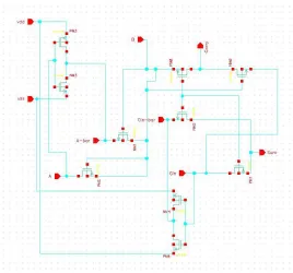
The following is the schematic of Full Adder based on Pass Transistor Logic technique using PMOS and NMOS. The circuit shows less number of transistor count and less power is dissipated.
Design of 1 bit Full Adder using GDI Technique:-
Gate Diffusion Input techniqueis a new level for low powered combinational circuits, this technique allows reducing delay time ,reducing powerconsumption and reducing area of the digital circuits so as to maintain less complexity of the logic design. GDI method is based on a simple cell shown in Figure.
GDI cell has three inputs G (Common gate input of small nMOS and pMOS), P (input to the source/drain of pMOS) and N (input to the source/drain of nMOS), bulk terminal of bothnMOS&pMOS is connected to N or P respectively. As gate diffusion input technique consumes less area on the silicon chip, resulting in less countof transistor, hence as area reduces in size, node capacitance value also reduces. Because of this the operating speed of gate diffusion input gate is more which indicates that GDI style is a better method to design a binary full adder. The threshold voltage in the GDI gate depends on voltage of source to bulk, to reduce the bulk effect the bulk terminal of pMOS and nMOS should be attached to their diffusion terminal, changes in threshold value due to change in voltage of source to bulk is called as Body Effect.
Fig -6: Gate Diffusion Input Cell
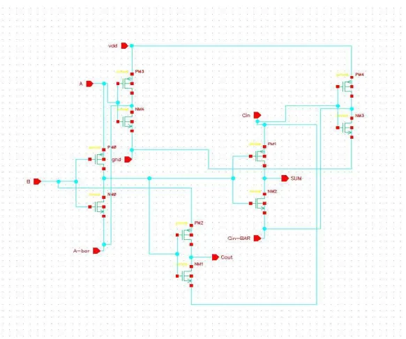
The following is the schematic of Full Adder using Gate Diffusion Input technique.
IV. RESULT AND CONCLUSION
The following figure shows the waveforms of 1bit Full Adder using Pass Transistor Logic technique. The waveform is square wave shaped. There are 3 input and 2 output waveforms.
Fig -8: Output Waveform of PTL based Full Adder
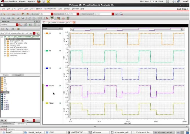
The following figure shows the waveforms of 1 bit Full Adder using Gate Diffusion Input technique. The waveform is square wave shaped. There are 3 input and 2 output waveforms.
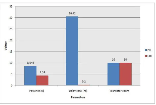
The two techniques GDI and PTL were compared on the basis of power dissipation, the time delay and amount of transistors used. The power and delay were calculated in milli-watt and nano-seconds respectively.GDI technique shows less amount of power dissipated and less delay. The same is shown in tabular form.
Techniques Power
(mW)
Delay(ns) Transistor
Count
PTL 8.546 30.42 10 GDI 4.34 0.2 10
Table-2: Comparison
The following figure shows comparison between GDI and PTL in graphical representation. The figure is a Bar-Graph representation of power, delay and transistor count based on both the techniques.
Fig -10: Graphical Representation
REFERENCES
[1] KorraRavi Kumar, P.Mahipal Reddy, M.Sadanandam, SanthoshKumar.A, M.Raju , “Design of 2T XOR gate based full adder using GDItechnique”, International Conference on Innovative Mechanism for Industry Application, 2017.
[2] ArkadiyMorgenshtein, Alexander Fish, Israel Wagner, “GDI A technique for low power design of digital circuits : Analysis and Characterization”, IEEE International Symposium on Circuits And Systems, 2017.
[3] S.Selvi, S.Pradeep, “6 Transistor Full Adder Circuit Using Pass Transistor Logic”, Journal of Chemical and Pharmaceutical Sciences, 2017. [4] Rita Mahajan, KshitijShant, “1-Bit Hybrid Full Adder by GDI and PTLTechnique”, International Journal Of Innovative Research in Computer
and Communication Engineering, 2016.
[5] Janardhan Reddy Gundam, M RamanaReddy ,“GDI Full Adder Using MUX-XOR Logic”, International Journal of Scientific Engineering and Technology Research, 2015.