A Dual Band Notched UWB Antenna with Optimized DGS Using
Genetic Algorithm
Mohammed C. Derbal*, Abdelbaki Zeghdoud, and Mourad Nedil
Abstract—An optimized dual-band notched antenna for Ultra-Wide Band applications, using the Genetic Algorithm (GA), is presented. By optimizing a Defected Ground Structure (DGS) in the ground plane of the UWB antenna, two notches are created at the desired frequency bands of 3.5 GHz and 5.8 GHz, respectively. A good agreement between the measurement and simulation results is observed. The optimized DGS shows good performance and accuracy compared to conventional approaches.
1. INTRODUCTION
Since the Federal Communication Commission (FCC) authorized the use of the bandwidth between 3.1 GHz and 10.6 GHz [1], UWB communication systems have drawn a lot of interest because of their advantages in terms of low cost for short range communication, low propagation power, high data rate, and remote sensing applications [2]. However, many other communication protocols may cause interference with the UWB range, such as the Worldwide Interoperability for Microwave Access in 3.3–3.7 GHz band and the Wireless Local Area Network (WLAN) in 5.15–5.825 GHz band [2].
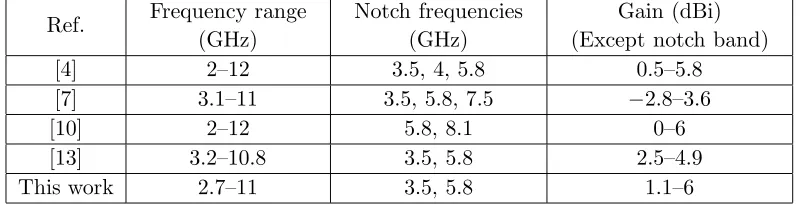
To avoid these interferences, various techniques have been suggested to design UWB antennas with band rejection capabilities [3–5]. In [3] an L shaped slot embedded at the center of the ground plane has been used to obtain two rejected bands. In [4], three different sizes of C-shaped slot are integrated with the radiating element to create band notches. Electrical Ring Resonators (EER) have also been suggested to achieve notched characteristics at desirable frequency bands [5]. Recently, other techniques including Defected Ground Structure (DGS) and electromagnetic bandgap (EBG) structure have been proposed [6–8]. In [6] a compact CPW-fed triple band-notched antenna was presented. By introducing a stepped impedance resonator-defected ground structure (SIR-DGS) and fork-shaped stubs, three sharp notches were achieved at frequencies of 3.5, 5.68, and 7.48 GHz. A monopole printed fork-shaped antenna for UWB applications with triple band-notched characteristics has been proposed in [7], and a U-shaped and two extended U-shaped defected ground structure (DGS) slots gave respectively two notched bands, 3.3 to 3.7 GHz for WiMAX and 7.1 to 7.76 GHz for downlink X-band satellite communication systems. A semi arc-shaped slot was etched on the radiating patch to notch the band from 5.15 to 5.825 GHz for WLAN applications. In [8], a uniplanar Electromagnetic Band Gap (EBG) structures was used to achieve a triple band-notched design. A dual notched band UWB monopole antenna was proposed in [9], and the band notches were achieved by introducing a meandered slot in the maple leaf shaped radiating element and U-shaped slot in feed line. In addition, a multiple-input multiple-output (MIMO) Vivaldi antenna with dual band-notched characteristics was presented in [10], and by adding a two split ring resonator (SRR) of different sizes next to the microstrip feed lines, dual notches were achieved to filter the interference of WLAN and X-band communication satellites. However, the drawbacks of these methods are poor notch width controlling and return loss criterion which is not accurately
Received 19 August 2019, Accepted 23 November 2019, Scheduled 16 December 2019
* Corresponding author: Mohammed Cherif Derbal ([email protected]).
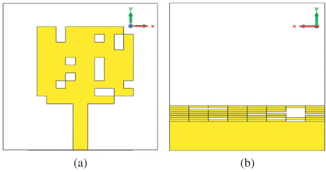
(a) (b)
Figure 1. Layout of the reference antenna, (a) top view, (b) back view.
To create the dual-band rejection at WiMAX and WLAN bands, a DGS is optimized in the ground plane of the reference antenna using GA. The algorithm will optimize the DGS on the rectangular unit cell of dimensions 4.3 mm×34.2 mm (Fig. 1(b)) in the ground plane. In fact, a part of the ground plane is divided into 8×8 pixels, which yieldsQ= 64 (whereQis the total number of pixels). Each pixel has a dimension of 4.28 mm×0.54 mm, where these values are obtained by trial and error. The presence and absence of pixels can be represented by a binary digit xq{0,1}, q = 1,2, ..., Q, which are grouped into a vector (sequence of digits) x={x1, x2, ..., xQ} to describe the configuration of the pixels in the rectangular cell.
First, the GA is used to optimize the DGS of the antenna to create one notched band at WiMAX band (3.5 GHz). The first step consists of generating a random population of matrix corresponding to different configurations of pixels. The population is composed of 40 different configurations of pixels in the rectangular cell per generation in all designs. Then, the next generation is formed from the previous one, and in this work, the number of generations used is 30. In the second step, the reflection coefficient of the generated populations is simulated, then compared with the desired result. This process is iteratively repeated until the reflection coefficient satisfies the antenna mismatching condition (S11>−3 dB) around the notched bands.
The GA cuts a random number of pixels from the rectangular cell in every iteration, and from 2Q different configurations ofx, the GA will determine thex corresponding to a solution that satisfies the desired specifications according to the following problem:
|S11(x, f)|>−3 dB When, f = 3.5
|S11(x, f)|<−10, otherwise
(a)
(b)
Figure 2. Layout of the optimized antenna for WiMAX rejection, (a) top view, (b) back view.
Figure 3. Simulated reflection coefficient of the reference antenna and the WiMAX band notched antenna.
The resulting structure of the antenna is shown in Fig. 2. Fig. 3 shows the simulated reflection coefficient of the one notched band optimized antenna. It can be seen that the optimized antenna covers the UWB from 3.1 to 10.6 GHz with the WiMAX band rejection.
The GA is then used to optimize the unit cells (Fig. 2(b)) to obtain two notches at the desired frequency bands of 3.5 GHz and 5.8 GHz, respectively, with a goal of return loss better than −3 dB in both bands according to the following problem:
|S11(x, f)|>−3 dB When, f = 3.5 GHz and f = 5.8 GHz
|S11(x, f)|<−10, otherwise
(2)
After a few hours of optimization, the algorithm is converged to the best solution, as illustrated in Fig. 4. The algorithm is developed using visual basic script and implemented in CST microwave studio.
3. RESULTS AND DISCUSSION
Figure 5 shows the simulated and measured reflection coefficients of the optimized dual band-notched antenna. It can be noticed that the measured reflection coefficient results agree well with the simulated ones. The optimized antenna covers the UWB, with two notched bands at 3.2–3.9 GHz (WiMAX) and 5.1–6.05 GHz (WLAN), respectively.
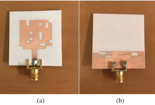
(a) (b)
Figure 4. Photograph of the optimized antenna, (a) top view, (b) back view.
Figure 5. Simulated and measured results of the reflection coefficient of the optimized antenna.
surface current is concentrated at the undesired frequency bands, thus, rejecting them by disturbing the path of the current. Fig. 6 illustrates the surface current distribution of the proposed antenna at both notched frequency bands. When the antenna operates at the frequency 3.5 GHz, most of the current is concentrated on the optimized DGS. In the same way, when the antenna operates at 5.8 GHz most of the current is also concentrated on the optimized DGS. Thus, the dual-notched bands are mainly caused by the optimized DGS.
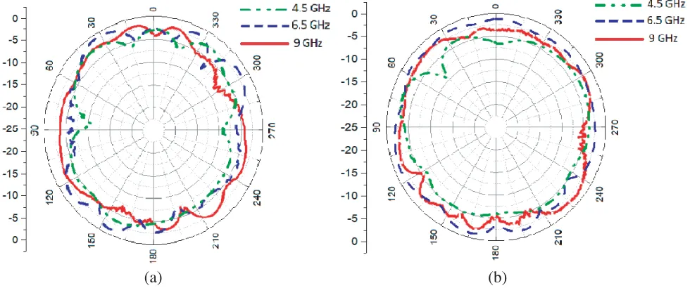
Figure 7 shows the measured radiation patterns of the proposed antenna in the E plane and H plane at three different frequencies 4.5 GHz, 6.5 GHz, and 9 GHz, respectively. It can be seen that the radiation patterns of the antenna are omnidirectional.
The simulated realized gains and efficiencies of the reference antenna and the proposed antenna are depicted in Fig. 8. From this figure, the reference antenna has a stable gain within the UWB from 3.1 to 10.6 GHz with a maximum gain of 6 dBi at 11 GHz. On the other hand, the gain of the proposed antenna decreases at the two notched bands with a gain of−0.5 dBi at 3.5 GHz and−1.7 dBi at 5.8 GHz. The efficiency at these notched bands drops to relatively lower values 25% and 20% at the frequencies of 3.5 GHz and 5.8 GHz, respectively, which validate the good performance of the optimized DGS to achieve a dual notched characteristic.
(a) (b)
Figure 6. Surface current distribution of the optimized antenna at both notched bands, (a) 3.5 GHz, (b) 5.8 GHz.
(a) (b)
Figure 7. Measured radiation patterns of the proposed antenna, (a)E plane, (b)H plane.
(a) (b)
A dual band notched UWB antenna has been proposed and optimized using the GA approach. By optimizing a Defected Ground Structure in the ground plane of the reference antenna using the GA, two notched bands are successfully achieved at the WiMAX and WLAN bands, respectively. The proposed method has demonstrated a good performance and accuracy to create band rejection and avoid the interference problem with UWB range. The proposed antenna is suitable for UWB communication systems.
REFERENCES
1. Chandel, R., A. K. Gautam, and K. Rambabu, “Tapered fed compact UWB MIMO-diversity antenna with dual band-notched characteristics,” IEEE Trans. Antennas Propag., Vol. 66, No. 4, 1677–1684, 2018.
2. Emadian, S. R. and J. Ahmadi-Shokouh, “Very small dual band-notched rectangular slot antenna with enhanced impedance bandwidth,”IEEE Trans. Antennas Propag., Vol. 63, No. 10, 4529–4534, 2015.
3. Zhang, Y. and C. Li, “Design of small dual band-notched UWB slot antenna,” Electronics Letters, Vol. 51, No. 22, 1727–1728, 2015.
4. Hammache, B., A. Messai, I. Messaoudene, and T. A. Denidni, “A compact ultra-wideband antenna with three C-shaped slots for notched band characteristics,” Microw. Opt. Technol. Lett., Vol. 61, No. 1, 275–279, 2019.
5. Vendik, I. B., A. Rusakov, K. Kanjanasit, J. Hong, and D. Filonov, “Ultrawideband (UWB) planar antenna with single-, dual-, and triple-band notched characteristic based on electric ring resonator,”
IEEE Antennas Wirel. Propag. Lett., Vol. 16, 1597–1600, 2017.
6. Zhang, C., J. Zhang, and L. Li, “Triple band-notched UWB antenna based on SIR-DGS and fork-shaped stubs,”Electronics Letters, Vol. 50, No. 2, 67–69, 2014.
7. Elhabchi, M., M. N. Srifi, and R. Touahni, “A tri-band-notched UWB planar monopole antenna using DGS and semi arc-shaped slot for WIMAX/WLAN/X-band rejection,” Progress
In Electromagnetics Research Letters, Vol. 70, 7–14, 2017.
8. Jaglan, N., B. K. Kanaujia, S. D. Gupta, and S. Srivastava, “Triple band notched UWB antenna design using electromagnetic band gap structures,” Progress In Electromagnetics Research C, Vol. 66, 139–147, 2016.
9. Iqbal, A., O. A. Saraereh, and S. K. Jaiswal, “Maple leaf shaped UWB monopole antenna with dual band notch functionality,”Progress In Electromagnetics Research C, Vol. 71, 169–175, 2017. 10. Li, Z., C. Yin, and X. Zhu, “Compact UWB MIMO Vivaldi antenna with dual band-notched
characteristics,” IEEE Access, Vol. 7, 38696–38701, 2019.
11. Fertas, K., K. Kimouche, M. Challal, F. Ghanem, F. Fertas, and R. Aksas, “Development of a novel UWB planar antenna using a genetic algorithm,” 2017 5th International Conference on Electrical
12. Derbal, M. C., A. Zeghdoud, and M. Nedil, “A novel dual band antenna design for WiFi applications using genetic algorithms,”2018 IEEE International Symposium on Antennas Propaga., 1009–1010, Boston, 2018.
13. Ibrahim, A. A., M. A. Abdalla, and A. Boutejdar, “A printed compact band-notched antenna using octagonal radiating patch and meander slot technique for UWB applications,” Progress In
![Figure 1 shows the layout of the reference antenna. It is designed and optimized using genetic algorithmsas reported in [11, 12] to cover the UWB](https://thumb-us.123doks.com/thumbv2/123dok_us/7732864.1266122/2.612.140.484.256.442/figure-reference-antenna-designed-optimized-genetic-algorithmsas-reported.webp)