1113 | P a g e
LOW POWER DESIGN OF CARRY SKIP BCD
SUBTRACTOR BY USING BCD ADDER
1
Mr. Prabu Venkateswaran ,
2Ms.Kalai Muthu .J
3
Ms. Krishnaveni .S,
4Ms.Mahalakshmi . S
1
Assistant Professor,
2, 3,4Students, Department of Electronics and Communication Engineering,
SNS College of Technology, Coimbatore. Tamilnadu, (India)
ABSTRACT
Computers commonly use binary number system for storing the data. Usually data is stored in the form of BCD
because of its higher level of accuracy than binary number system. Though it cannot be as efficient as binary
floating point in many aspects, representing in BCD leads to simplification and ease of computation. The
amazing fact about BCD used as most of calculation process like calculator i.e. in both scientific and
engineering versions. Firstly, we showed a modified design of conventional BCD subtractor and also proposed
designs of carry skip BCD subtractor . The proposed designs of carry skip BCD subtractor are based on the
novel designs of carry skip BCD adders, respectively. The BCD Design is implemented by using Xilinx and to
analysis the power of the adder.
Keywords
:
Full adder, Nine’s complement, BCD adder, BCD subtractor .
I.
INTRODUCTION
Recently, specifications for decimal floating point arithmetic have been added to the draft revision of IEEE-754
standard for floating point arithmetic.Despite the widespread use of binary arithmetic, decimal computation
remains essential for many applications. Not only is it required whenever numbers are presented for human
inspection, but is also often a necessity when fractions are involved. Decimal fractions are pervasive in human
endeavors, yet most cannot be represented by binary fractions. The value 0.1 for example, 75 requires an
infinitely recurring binary number. If a binary approximation is used instead of an exact decimal fraction, results
can be incorrect even if subsequent arithmetic is correct. As the IEEE standard for decimal floating point is approved, hardware In the BCD subtraction, the nine‟s complement of the support for decimal floating point
arithmetic will be incorporated in processors for various applications. Still, a major consideration while
implementing Binary Coded Decimal (BCD) arithmetic is to enhance its speed as much as possible.
II
RELATED
WORK
In the BCD subtraction, the nine‟s complement of the subtrahend is added to the minuend In the BCD arithmetic, the nine‟s complement is computed by nine minus the number whose nine‟s complement is to be
computed. This can be illustrated as the nine‟s complement of 5 will be 4 (9-5= 4), which can be represented in
1114 | P a g e
The Nine‟s Complement Gate is a 5*5 reversible gate and its logic representation is shown in Fig 1. One input
of this gate is the control signal. Based on the bit information at control signal (i.e. 0 or 1) either the input or
nines complement of the input is passed to the output pin Q, R, S, T. The features of nine complement are given
below.
Fig 1. Block diagram of NCG (Nine Complement Gate).
Fig. 2 Nine’s Complementer
In BCD arithmetic, instead of subtracting the number from nine, the nine‟s complement of a number is determined by adding 1010 (Decimal 10) to the one‟s complement of the number. The nine‟s complementer
circuit using a 4-bit adder and XOR gates is shown in Fig.2. We have realized that there is no need to use XOR
gates in the nine‟s complementer for complementing. The use of NOT gates will better suit the purpose and will
reduce the complexity of the circuit,in CMOS.
III. PROPOSED SYSTEM
In order to design the carry skip equivalent of the BCD subtractor, we propose the carry skip equivalent design
1115 | P a g e
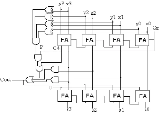
Fig.3 Proposed Carry Skip BCD Adder
3.1 Carry Skip BCD Adder
In this paper, we proposed the design of carry skip BCD adder. It is constructed in such a way that the first full
adder block consisting of 4 full adders can generate the output carry „Cout‟ instantaneously, depending on the input signals and „Cin‟. This avoids carry to be propagated in the ripple carry fashion. Figure 3 shows the
proposed carry skip BCD adder. The working of the proposed carry skip BCD adder can be explained in this
manner: In the single bit full adder operation, if either input is a logic „1‟, the cell will perform in the way that
the carry input is given to its carry output. Hence, the ith full adder carry input Ci, will propagate to its carry
output Ci+1 when Pi= Xi Yi, where Xi and Yi represents the input signal to the ith full adder. Thus, the four
full adders at the first level will make a block that can generate a propagating signal „P‟. When „P‟ is „1‟, it
will make the block carry input as „Cin‟, to propagate the carry output as „Cout‟ of the BCD adder, without
waiting for the actual propagation of carry in the ripple carry manner. An AND gate is used to generate a block propagate signal „P‟. Depending on the value of „Cout‟, appropriate action is taken. When „Cout‟ is equal to
one, binary 0110 is added to the binary sum (correction logic to convert sum in BCD format) using another 4-bit
binary adder at the second level or bottom level, as shown in Fig.3. The output carry generated from the bottom
binary adder is ignored, since it supplies information already available at the output carry terminal.
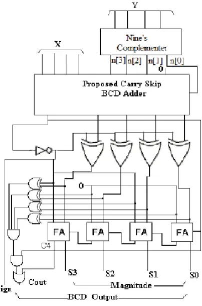
3.2 Carry Skip BCD Subtractor
Figure 4 shows our proposed design of the carry skip BCD subtractor. It is to be noted that the carry skip implementation of the nine‟s complementer in the proposed circuit will not be beneficial.When the input carry
Cin=1, the skipping property of the BCD adder is effectively benefited. Thus, in order to extract the benefit of
the carry skip property of the BCD adder in the proposed BCD subtractor, we have made the LSB output (n[0])
of the nine‟s complementer as input carry „Cin‟ of the carry skip BCD adder and passed „0‟ in its place for
1116 | P a g e
adder will be X+(n[3]n[2]n[1]‟0‟)+n[0], where n[0] will work as Cin. The last block of the 4-bit adder in the
proposed circuit has also been designed in the carry skip manner to further improve the efficiency of the
proposed design. This will result in the generation of Cout in Fig.4 in carry skip fashion. As far as existing
literature and our knowledge are concerned, the proposed circuit is the maiden attempt to provide the carry skip
equivalent of the conventional BCD subtractor.
Fig4. Proposed Carry Skip BCD Subtractor
IV. SIMULATION OUTPUT
1117 | P a g e
V CONCLUSION
In this work, we have proposed carry skip BCD subtractors based on novel designs of carry look-ahead and
carry skip BCD adders, respectively. In this paper an optimized one digit BCD adder and an optimized one digit
carry skip BCD adder are presented.It is shown that the proposal is highly optimized in terms of the number of
reversible logic gates, the number of garbage outputs and the delay involved. The delays involved invarious
circuits in the existing papers are calculated on the similar lines. The design method is definitely useful for the
construction of future computers and other computational structures also it is useful for future computing
techniques like ultra low power digital circuits and quantum computers. Optimization of other computational
circuits is under investigation as a future work.
REFERENCE
[1] Majid Mohammadi, Mohammad Eshghi, Majid Haghparast and Abbas Bahrololoom, (2008) “Design and
Optimization of Reversible BCD Adder/Subtractor Circuit for Quantum and Nanotechnology Based
Systems”, World Applied Sciences Journal, vol. 4, no. 6, pp. 787-792.
[2] V.Singaravelan ,P.Kannan and S.Prabu Venteswaran,”Design of Multiplier Architecture By Using Multioutput Adder”,in International Journal of ModernTrends in Engineering and Science(IJMTES), Vol
04,ISSN:2348-3121,Jan 2017.
[3] H.R.Bhagyalakshmi and M.K.Venkatesha, „Optimize[d reversible BCD adder using new reversible logic
gates‟, Journal of Computing, Volume 2, Issue 2, February 2010, ISSN 2151-9617 arXiv:1002.3994v1.
[4] Hafiz Md. Hasan Babu and A. R. Chowdhury, "Design of a Reversible Binary Coded Decimal Adder by
Using Reversible 4-bit Parallel adder", VLSI Design 2005, pp-255-260, Kolkata, India, Jan 2005.
[5] Haghparast M. and K. Navi, 2008. A Novel reversible BCD adder for nanotechnology based systems.
Am. J. Applied Sci., 5 (3): 282- 288.
[6] Cowlishaw, M.F.: Decimal Floating-Point: Algorithm for Computers. In: Proceedings 16th IEEE
Symposium on Computer Arithmetic, pp. 104–111 (June 2003)
[7] Landauer, R.: Irreversibility and Heat Generation in the Computational Process. IBM Journal of
Research and Development 5, 183–191 (1961).
[8] Bennett, C.H.: Logical Reversibility of Computation. IBM J. Research and Development, 525 –532
(November 1973)
[9] Vedral, V., Bareno, A., Artur, E.: Quantum Networks for Elementary Arithmetic Operations
(November 1995) arXiv:quant-ph/9511018 v17.
[10] Thapliyal, H., Srinivas, M.B.: Novel Reversible TSG Gate and Its Application for Designing
Reversible Carry Look Ahead Adder and Other Adder Architectures. In: Proceedings 10th Asia-Pacific
Computer Systems Architecture Conference (ACSAC 2005). Lecture Notes of Computer Science,
vol. 3740, pp. 775–786. Springer, Heidelberg (2005)
[11] Thapliyal, H., Kotiyal, S., Srinivas, M.B.: Novel BCD Adders and their Reversible Logic
1118 | P a g e
VLSI Design and 5th International Conference on Embedded Systems (VLSI Design 2006), Hyderabad
(VLSI Design 2006), January 4-7, pp. 387–392 (2006)
[12] Fredkin, E., Toffoli, T.: Conservative Logic. International Journal of Theor y. Physics, 219–253 (1982)
[13] Toffoli, T.: Reversible Computing. Tech. memo MIT/LCS/TM-151. MIT Lab for Computer Science
(1980)