ABSTRACT
ROHRBAUGH, NATHANIEL W. Improving the Performance of Semiconductor Sensor Devices Using Surface Functionalization. (Under the direction of Dr. Albena Ivanisevic.)
Signals of AlGaN/GaN FETs were measured as IDrain values and in the earliest study an average signal increase of 96.43% was observed when surfaces were incubated in a solution of a known recognition peptide sequence (SVSVGMKPSPRP). This work showed that even without a form of surface modification the devices were capable of generating a response in the presence of a charged biomolecule. Solution exposure tests done devices showed that incubating peptides on the device surfaces produced a weak interaction and following 24 hrs of soaking no signs of peptide remained via XPS analysis.
Subsequent testing was done to incorporate the phosphonic acid functionalization techniques shown previously by other members of this lab to the AlGaN/GaN surfaces as a remedy to this solution instability. In this second study FETs were modified using a heated phosphoric acid:ethephon etch followed by an incubation in TAT-C peptide. Resulting IV measurements done on the samples showed a shift in threshold voltage of the FETs following the etching procedure followed by a recovery of this shift from prolonged solution exposure. In total samples were given 168 hours of soaking and showed persistent peptide presence through the N 1s peak from XPS scans.
FETs modified with this phosphonic acid derivative were examined in a third study under a simulated pollutant sensing scenario by measuring varied concentrations of Hg via a phytochelatin peptide bound to FET surfaces. HNO3 used in the Hg stock solution led to degradation of the FET signal but did not remove the phytochelatin layer. This led to a compensation effect in sensing the highest levels of Hg, lower concentrations however were successfully tested and showed varied responses from the FETs relative to the Hg content.
noted from the addition of a biological fouling solution to the FETs and an increase in this effect when the biofouling was done to a phosphonic modified FET surface. Additionally devices were modified and soaked for 5 weeks and showed no shift or degradation in signal. Lastly in controlling for gate width of the FET it was found that the shorter 50 μm gates were more susceptible to environmental interference than the 100 and 150 μm gated devices.
Improving the Performance of Semiconductor Sensor Devices Using Surface Functionalization
by
Nathaniel W Rohrbaugh
A dissertation submitted to the Graduate Faculty of North Carolina State University
in partial fulfillment of the requirements for the degree of
Doctor of Philosophy
Materials Science and Engineering
Raleigh, North Carolina 2016
APPROVED BY:
______________________________ _______________________________
Committee Chair Committee Member
_______________________________ _______________________________
Committee Member Committee Member
Dr. Albena Ivanisevic Dr. Ramon Collazo
BIOGRAPHY
Nathaniel Wilday Rohrbaugh was born on October 27th, 1990 in Raleigh, North Carolina to parents Richard and Susie. Nathaniel attended Green Hope High School in Cary, NC and graduated in 2009. During his time there he partook in distance running events on the cross country and track teams for four years and becoming a captain of the cross country team in his final year. In addition to these events Nathaniel was a leader of the Green Hope FCA, and worked in the tech theatre department on the set building team that won Wake County’s Outstanding Set Design in 2009.
After graduating Nathaniel went on to attend North Carolina State University in the Materials Science and Engineering Department. During his time there he partook in summer undergraduate research for all years of his time there through the research group of Dr. Jerome Cuomo. He worked on several consulting projects and worked on plasma deposition projects with other graduate students, and seed germination studies on atmospheric plasma.. After completing a bachelor’s degree in science from North Carolina State he began his
ACKNOWLEDGMENTS
My biggest thanks go to out to my advisor, Dr. Albena Ivanisevic for a multitude of reasons. Her patience, support, and guidance helped keep me on track and able to graduate with a Ph.D in less than four years. Without my time in her group I don’t think I would be
able to leave as confident in my perspectives and understandings of designing and operating experiments in a lab setting as I am now. I would additionally like to thank my committee members: Ramon Collazo, for the access, cooperation, and support he provided to my research and the greater exposure to the world of III-nitrides and growth I gained from it; Dr. Lew Reynolds, who brought insight and a more critical look at my findings, and for consistently having some of the most interesting and engaging classes in our department; and Dr. Jan Genzer, for also providing a non-MSE perspective on the science I have been learning, and thus making me learn about a field of interface science I would not normally have been exposed to. Another thank you to Dr. Yara Yingling who in particular helped give me insight when I was starting graduate school.
More thanks to those who welcomed me into my the research group when I joined including both Stewart Wilkins and Lauren Bain. Stewart I can thank for helping to feed my motorcycle obsession and Lauren for finally having someone to relate to on the nuances of baking, food, and annoying Brady. My later group members and friends as well including Nora Berg, Brady Pearce, and Patrick Snyder. All of you I would call good friends have made my time in this group worthwhile and enjoyable both in and outside of work. Other people that I’ve had the pleasure of sharing an office or time with at work like Dr. Christer
To the GSA folk and all the times I got to serve the department in a more social and fun sense like buying beer or organizing dinners and chili cook-offs. The folks in RB1 including Dr. Ronnie Kirste, Felix Kaess, and most of all the Bryan twins Isaac, and Zach. The twins in particular deserve so much more credit than they received for the work they did for me and their coworkers, and both are wonderful individuals who I am glad I was able to share a camping trip with. All of these people helped make my time in the MSE department more enjoyable, enlightening, and supportive and I am thankful for all of you.
Special thanks to Dr. Jerome Cuomo for all the support, conversations, and opportunities to expose me to a laboratory environment very early on in my college career. These years truly helped shape me into the more curious engineer that I am today, in addition to getting to work with such a passionate and knowledgeable professor as Dr. Cuomo.
Lastly, I’d like to thank my family and friends for their support over the years, and
TABLE OF CONTENTS
LIST OF TABLES……….viii
LIST OF FIGURES………...ix
Chapter 1 Stability and Reliability of III-Nitride Based Biosensor………..1
1.1 III-Nitride Materials……….1
1.2 Doping of nitrides……….4
1.3 Water stability resistance to etching and degradation……….9
1.4 Toxicity……….12
1.5 Biocompatibility………16
1.6 Chemical functionalization………19
1.6.1 Aluminum Nitride………..19
1.6.2 Gallium Nitride………..20
1.6.3 Aluminum Gallium Nitride………24
1.7 Sensing devices………..24
1.8 FET Behavior……….30
1.9 Analytes/receptors………..33
1.10 III-nitride FET biosensor stability………..………..36
1.11 Unmet Needs………41
Chapter 2 AlGaN/GaN Field Effect Transistors Functionalized with Recognition Peptides………..……….44
2.1 Summary………44
2.2 Introduction………...…….44
2.3 Experimental………..46
2.4 Sensing response to incubated biomolecules……….48
2.5 Aqueous stability………51
2.6 Particulate interference………...53
Chapter 3 Longer term stability assessment of AlGaN/GaN field effect transistors modified with peptides; a comparison of device characteristics versus surface properties………...56
3.1 Summary………56
3.2 Introduction………56
3.3 Experimental and chemical functionalization………58
3.4 Functionalized AlGaN/GaN topography………60
3.5 Conductivity response………61
3.6 Surface peptide stability……….64
Chapter 4 HgNO3 Sensitivity of AlGaN/GaN Field Effect Transistors Functionalized with Phytochelating Peptides………67
4.1 Summary………....67
4.2 Introduction………67
4.3 Experimental………..69
4.4 XPS Surface confirmation………..70
4.6 Concentration sensing of Hg………..75
Chapter 5 Biofouling and long-term solution exposure stability of phosphonic acid derivative modified AlGaN/GaN Field Effect Transistors………76
5.1 Summary………76
5.2 Introduction………76
5.3 Experimental and biofouling procedures………78
5.4 Long term solution exposure………..82
5.5 Biofouling and phosphonic acid derivative effects………82
5.6 Gate width dependency of response……….………..84
Chapter 6 Conclusions and Future Outlook……….85
6.1 Conclusions………85
6.1.1 Chapter 2………85
6.1.2 Chapter 3………85
6.1.3 Chapter 4………87
6.1.4 Chapter 5………89
LIST OF TABLES Table Number and Caption
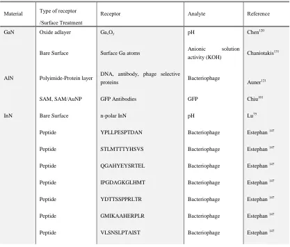
1.1 Example analyte and receptor pairings shown for III-nitride compounds used in biological or non-biological sensing devices. Beneath the receptor information indicates the molecule or compound that acts as a receiving component of a sensing scheme, and the analyte represents the aqueous or environmental stimuli that interact with the III-nitride surface groups.
2.1 List of adsorbates utilized in this study
LIST OF FIGURES Figure Number and Caption
1.1 Example diagrams of both Zinc Blende and Wurtzite structures seen in III-nitride
compounds.
1.2 Figure 1. Cell growth on various GaN surfaces; A) and B) fibroblast growth on GaN using SAM modified surfaces, adapted with permissions from Faucheux et al.1, C) and D) neuron growth on GaN using modified surface topographies, adapted with permission from Bain et
al.2, E) and F) neuron cell growth using IKVAV binding proteins on GaN, adapted with permissions from Jewett et al.3
1.3 A) Basic chemisorption functionalization with analine following ion bombardment of GaN surfaces under UHV conditions.4 B) Example of organosilane surface
attachment following hydroxide termination to the surface, using the forementioned TUBTS molecule.5 C) Example of a Grignard reagent attachment to GaN using a chlorine terminated surface.6
1.4 Schematic of biomolecule functionalized AlGaN/GaN FET. Adapted with the
permission from Rohrbaugh et al.54
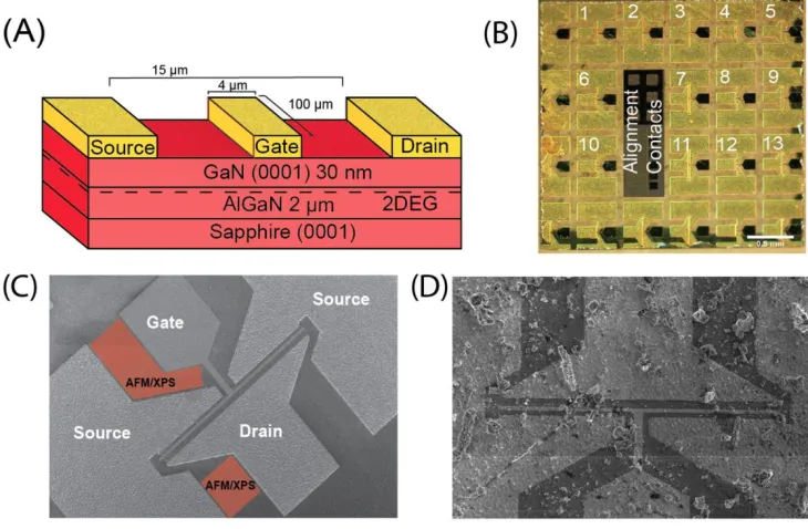
1.5 Top down view of an FET used in the studies described in this work. Shown are the source, drain and gate regions. Additional dimensions shown are the gate length and gate width. Gate length being held at a constant 15 μm across all samples, and gate width being either 50, 100, or 150 (shown above) μm.
1.6 Testing methods and objectives of the different properties that make up the stability of a biological sensor.
2.2 (a) X-ray photoelectron spectroscopy analysis of clean devices, RP modified and RP modified devices after soaking in solution. (b) Drain current changes of devices modified with all adsorbates. (c) Drain current changes of devices modified with all adsorbates after soaking in solution.
2.3 Full sample set of percent changes observed for the RP modified FET groups. Three samples were removed for XPS analysis.
2.4 Change in drain current of devices modified with RP and exposed to GaN powder slurry.
3.1 Functionalization scheme of AlGaN/GaN FET surfaces through an in-situ functionalization with phosphoric acid and ethephon followed by incubation in a cysteine terminated peptide.
3.2 Representative AFM images of peptide surfaces at different stages in the solution exposure process. a) peptide terminated device surface prior to soaking in water; peptide agglomerates can be seen as white spots along surface; RMS Roughness of 1.41 ± 0.3 nm, and a maximum surface feature height of 39.3 nm. b) Device surface after 24 hrs of water soaking; fewer particulates and an increase in small defects count are observed; RMS Roughness of 1.89 ± 0.4 nm, and a maximum surface height of 71.2 nm. c) Poly lysine device surfaces demonstrating an excessively thick and relatively smooth biofilm; RMS Roughness of 3.2 ± 0.4 nm, and a maximum surface feature height of 16.9 nm.
3.3 a) Gate voltage sweep data for control groups including the etched, pristine, ethephon functionalized and poly lysine sample sets. b) Gate voltage sweep data for soaking stages starting at 24 hrs and going up to 168 hrs. Lines on both parts of the figure represent average value over an entire sample group, and shaded regions represent +/- 1 standard deviation.
4.1 a) Ethephon and phosphoric acid surface functionalization, b) Peptide incubation resulting in covalent binding between peptide chains and AlGaN/GaN FET surfaces, c) Hg standard solution exposure to Hg-sensitive peptide functionalized AlGaN/GaN FETs.
4.2 XPS spectra of cleaned surfaces, peptide functionalized, 1, 10,100 and 1000 ppm Hg confirming lack of amide and Hg peaks prior to the functionalization steps and affirming the diminishing Hg peaks as concentration was stepped down. 4.3 a) Three control groups testing the effects of the different solution treatments
performed in this experiment including a water control, full ethephon
functionalization, and then full functionalization plus the undiluted Hg stock solution. b) Comparison of water, 1000 ppm, and 10 ppm effects on functionalized samples and the negative peptide control using TAT-C.
4.4 IDresponse of phytochelatin modified AlGaN/GaN FETs exposed to varying concentrations of Hg in nitric acid solution. Each bar represents a single chip containing a maximum of 13 individual FETs. Significant differences exist between these groups indicating a sensitivity to varying Hg concentration within the solution. 5.1 Scheme outlining the functionalization and treatment of the AlGaN/GaN FETs
throughout the experimentation. a) groups of FETs are functionalized in either PP or PFB. b) FETs are soaked in either a long term DI water solution or biofouling solution. c) FETs are removed, dried, and tested for ID signal response.
5.2 Comparison of ID response at peak transconductance of each sample group. a) Shows shifting ID signal from the initial untreated phase of the study up to the etched and functionalized phase including a 5 week soak test and a BSA fluid soak test. b) Shows the shift in ID from the functionalization phase of the study until the final soaking and testing of each sample group, BSA control was tested again from the same setup in part a) for comparison.
CHAPTER 1
Stability and Reliability of III-Nitride Based Biosensors
1.1. III-Nitride Materials
Two particular materials of significant interest within recent years have been AlGaN and
GaN. These two materials are commonly combined in a heterojunction structure for high electron
mobility transistors (HEMT). From a biological compatibility stand point the AlGaN/GaN system has
been shown to be non-toxic when put under physiological conditions as well as maintaining a
chemically stable surface.7 Furthermore cellular growth studies have revealed that AlGaN/GaN is a suitable surface for cell growth and tissue interfacing.8 These devices are fabricated such that layered AlGaN/GaN produces a conductive channel at their interface, close to the sensing surface. It is this
interface that gives this material its characteristic properties as a biosensing platform, and allows for
quantification of dissolved or airborne compounds. Interactions between the surface of the
AlGaN/GaN device and its environment generate changes in along the surface that influence the
conductive channel.9 The electrical fields of these interactions produce conductance changes in the channel, thus these devices fall under the category of field effect transistors (FETs). One of the largest
benefits of the AlGaN/GaN system is the adaptability of the surface to different modification and
functionalization schemes. This is made possible by the availability of surface bonding sites and the
innate chemical inactivity in the presence of both acidic and basic solutions.10 Thus, combining the benefits of physiological stability, sensitivity to surface interactions, and wide range of surface
modifications the AlGaN/GaN system is one of the most widely used III-nitride currently being used
in biosensor research and development. While the AlGaN/GaN system provides an excellent example
III-nitrides. AlN, GaN, InN all share similar surface properties and have been examined as possible base
materials for novel biosensing platforms.
In this chapter we will be discussing III-nitrides for biosensing as a wider field of study.
Although there will be a large amount of focus given to AlGaN/GaN as the most prominent III-nitride
of study in literature for biosensing, other less commonly used III-nitrides will be explored as well.
Specific biosensor device functionality, specificity, selectivity and operation will be discussed on a
material by material basis. Additionally, a background into the materials themselves will be provided
from a stability perspective with regard to solution exposure, doping, and interactions with biological
systems.
The group III-Nitrides can be defined as the class of materials that encompasses all
compounds formed between a III group element binding with nitrogen. This includes AlN, GaN, InN,
InGaN, and AlGaN; as well as all other binary, tertiary, and quaternary combinations. Interest has
greatly increased in the past decades as the need for light emitting diodes (LEDs) and other
optoelectronics has risen. III-Nitrides offer both wide bandgap semiconductor materials like GaN and
AlN, as well as narrow bandgap materials like InN.11,12,13 It is due to this wide bandgap character that these materials have taken such an interest for optoelectronics. 14 The bandgap can be tuned depending on the alloy compositions, or other factors induced during processing such as strain.15,16 All of these materials have a direct bandgap making them attractive for light emission and detector
applications.17
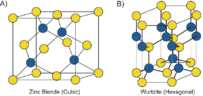
III-nitride materials may crystallize into two structures: wurtzite (hexagonal) and zinc blende
(cubic). Example diagrams of both wurtzite and zinc blende can be seen in Figure 1. Wurtzite is the
in the a and c directions.18 Anisotropic behavior exists between the a and c directions.19 Polarization is inherent to the wurtzite structure of the III-nitrides and can be categorized as either spontaneous
and piezoelectric. Spontaneous polarization comes from electric fields generated between alternating
layers of N and III group metal in the material and the non-centro symmetry of the hexagonal crystal
structure.20 Zinc blende structures have similar alternating layers to wurtzite but lacks this spontaneous polarization due to the lack of non-centro symmetry. Piezoelectric polarization arises
from stresses on the III-nitride material.20 Typical heteroepitaxy used for these materials results in strain; therefore both polarization effects will always be present in III-nitride deposited layers.
III-nitrides films are typically grown in the +c orientation of the crystal with the surface being the
(0001) plane. Due to the non-centrosymmetric nature of the hexagonal structure, two different
orientations of the crystal lattice are possible along the c-axis. Thus the crystal can be grown in the +c
orientation (0001) referred to as the III (either Ga, In or Al)-polar and the –c orientation (000-1)
referred to as the N-polar.21 This orientation also determines the direction of the spontaneous polarization of the crystal, thus referring to its polarity orientation. The corresponding polarity
determines the possible surface reconstructions available for the c-planes, or simply the number of
dangling bonds available on the surface.22 In the III-polar case, a negative polarization charge at the surface induces a positively charged depletion region near the surface, while for the N-polar surface a
positive polarization charge induces a negatively charge region. This negative charge region arises
from accumulation of free carrier or a change in the occupation of the surface states. Polarization
differences across interfaces between III-nitride layers determine the induce charge at that interface.
Such an example is the polarization discontinuity found between the AlGaN/GaN interfaces where
is the basis for the formation of the conductive channel in the field effect transistors previously
described and as such they are typically described as high electron mobility transistors (HEMT).
Figure 1.1. Example diagrams of both Zinc Blende and Wurtzite structures seen in III-nitride compounds.
1.2. Doping of nitrides
Doping of III-nitride materials has become more common practice in recent years and can be
incorporated into the MOCVD growth processes.16 The addition of dopants to these films allows for tunable conductivity characteristics and selection of the charge carrier type that will be dominant in
the film.23 When defining doping charge carriers, n-type refers to electrons dominating, and p-type being hole dominated conduction. Dopants of a higher valence than the base material, in this case
group IV, are added to generate n-type behavior. In contrast, for hole dominated films a lower valence
dopant is added, such as a group II material. Depending on the charge carrier type, either donor or
acceptor states will be created within the bandgap of a semiconducting material.24 However, effective doping is only possible if the activation energy of the charge carriers is low enough to provide free
electrons or holes with sufficient amounts at room temperature. Here, the activation energy is defined
as the energy that is needed to detach a carrier from its dopant. Since this energy is typically provided
around 27 meV at room temperature. Furthermore, compensation of dopants due to incorporation of
unwanted charged point defects needs to be controlled. This highlights the need to find shallow
dopant and control compensation in III-Nitrides.
Most common dopants in GaN and its ternary materials are Si for n-type behavior and Mg for
p-type. These provide good representation for doping in this material system as both are widely used
and well researched for III-nitride materials. Si is a shallow donor in GaN with an activation energy
of 12 meV. For Si doped GaN a good controllability has been found and free carrier concentrations
ranging from 1×1016 cm-3 to 5×1019 cm-3 have been demonstrated. Higher free carrier concentrations can be targeted with Ge if needed. However, p-type doping with Mg is found to be more
difficult.24,25 This can be related to the higher activation energy of the Mg-acceptor of 160 meV, the formation of Mg-H complexes and passivation after growth , and limitations in the doping capabilities
due to self-compensation for Mg>3×1019 cm-3.24,26 While the Mg-H complex can be activated following fabrication with an additional annealing step in an H free atmosphere and compensation
can be controlled using advanced point defect control mechanisms, the activation energy stays the
main limiting factor.27 Consequently, typical free carrier concentrations of MOCVD grown GaN:Mg are in the range of 3-6×1017 cm-3 for 3×1019 cm-3 acceptors. Thus, the conductivity of Mg p-type doping as a whole is relatively low given the above factors when compared to the capabilities of Si
n-type doping.28,23
Doping in the other binary III-nitride systems is based on the results and experience from
GaN. N-type behavior in AlN has been shown with Si but doping capabilities are limited due the
formation of a DX-center and increase of the activation energy to >200 meV.29 P-doping using Mg has been tried in AlN as well, but no free holes or p-conductivity has been demonstrated as of
today. InN possesses native n-type behavior in many cases due to its surface high electron
more accessible to dopants due to its smaller atomic radii as shown in work involving Si and
Mg.35,36,37 Nuances of doping for each of these binary compounds are beyond the scope of this work and is still a field where new up and coming research is being done. As such for more information on
doping effects on stability of biosensors readers are encouraged to investigate further with some of
the references provided here.
III-nitride ternary compounds are unique from a doping perspective in that both Group III
elements in the ternary compound can be treated as dopants of each other depending on desired
characteristics and tuning of the desired final structure. Similar to literature mentioned previously on
binary III-nitrides research within this field is broad and as such only n-type AlGaN will be discussed
in a briefly as an example. N-type doping of low Al-content AlGaN has been shown using Si and
provides a good example of the balancing that must be done with the two III-group elements in the
final product. In work done by Collazo et al, AlGaN with varying ratios of Al to Ga are explored
relative to their Si doped n-type behavior.38 The activation energies of Si impurity formation within GaN and AlN are approximately 17 meV and 200 meV respectively.39 Thus, as Al content increases in AlGaN a drop off in n-type behavior is observed resulting in almost complete removal of the
behavior at Al0.8Ga0.2N.38 This decrease in n-type behavior can be further explained by DX center
formation and vacancy-complex compensation within the AlGaN. More information into AlGaN’s
conductive properties and performance relative to growth processes and doping can be found in the
extensive review on the subject in Jones et al.16
In discussing the environmental stability that doped III-nitride materials possess a definition
of shallow and deep dopants needs to be established. Shallow dopants like that of Si donors in GaN
have relatively small activation energies which can be filled from thermal energy within the
once the III-nitride compound is in a conducting mode. Deep dopants however, require a much
greater energy to ionize and in many cases will not provide free charge carriers to aid in conduction.16 Dopants such as these provide compensating centers that can act as recombination sites for electrons
and holes, and are commonly referred to as charge carrier traps.41
Doped GaN, both n-type and p-type, experiences a carrier removal or relocation when
exposed to neutron radiation that varies on the type of charge carrier.42 The methodology of quantifying radiation damage takes into account the number of carriers that no longer contribute to
the overall n-type or p-type behavior. This is typically because the carrier or dopant has been moved
to a dislocation site within the lattice. In this study by Pearton et al. carrier removal rates were 20
times higher for p-type doping than in n-type doping, however both methods had removal rates >103 cm-1 under proton radiation doses of 1014 cm2.42 Under the same testing neutron and electron radiation were examined with neutron radiation having a weaker removal rate. The rate of removal for neutron
radiation was <102 - 100 cm-1 however, electron radiation yielded a weaker removal at <101 – 10-1 cm
-1
over a wider range of dosages. The generation of electron traps within the GaN layers leads to a
Fermi level pinning effect (reported at a conduction band energy of -0.95 eV) which can lead to
self-compensating effects for conductivity.43 In general under radiation dosing n-GaN has been observed to become semi-insulating as carriers are displaced. The problem presents itself with AlxGa1-xN
heterojunction layers at various levels of Al doping. The self-compensating effects of radiation
damage manifested itself here as an overall increase in resistivity of the GaN layers in AlGaN/GaN
heterostructures.44 This increase in resistivity resulted in degradation of the 2DEG in both AlGaN/GaN interfaces and AlN/GaN interfaces, and is largely attributed to the increase in defect
density causing a drop in mobility. Cited values for the drop in conductance were as high as 50% for
of 2DEG layers under such conditions.42 It was observed that with increasing Al content in AlGaN/GaN heterostructures (up to Al0.5Ga0.5N) an increase in trap concentration was observed
which in turn lead to decreases in the carrier mobility and conductance of the device.45 Similar effects were observed in proton irradiated samples of AlGaN/GaN as well.46 Thus it can be said that radiation effects are of significant concern for GaN based devices and heterostructures if the intended end use
requires reliable performance under prolonged and elevated radiation exposure. In context of
electrical stability these effects stand out and may present problems over time, but there are ways to
mitigate these effects by lowering initial dislocation densities in GaN based materials.43 There is also evidence for recovery and relaxation of radiation induced carrier migration over time after following
a strong radiation exposure.47
Despite these findings, III-nitrides when compared to other materials have shown evidence of
significantly higher radiation hardness.48 In terms of overall resilience both AlGaN and GaN shown radiation hardness values less than but comparable to diamond.49,48 AlN has been further investigated for creating resistant layers from UV up to gamma radiation.50,51,52 In this work done by Tittmann et al. AlN showed high resilience when exposed to 5.8 x 10¹⁸ neutrons cm-2 and 26.8 MGy gamma radiation, this was quantified by the lack of change in AlN’s piezoelectric properties.51
InN has not
been as widely studied for radiation hardness but has shown interesting responses in relation to charge
carrier removal. N-type InN demonstrates an opposite effect to GaN and other III-nitride compounds
in that it shows an increase in carrier concentration once exposed to high levels of radiation. This can
be explained by the high electron accumulation that occurs in InN and the innate n-type behavior that
comes from higher defect densities.53 Highly crystalline InN nanowires exhibit minimal electron accumulation, thus defects brought on by radiation damage increase this accumulation and
properties. In this same study by Emtsev et al. annealing of InN and GaN allowed for a recovery of
properties to values similar to previous measurements done before the radiation treatments.53 Annealing GaN required temperatures greater than 600°C before substantial electron mobility and
charge carrier concentrations recovered. InN showed opposite effects as a reduction in mobility was
observed at temperatures between 400° and 500°C. Once temperatures exceeded 500°C electron
mobility began to return to that of pre-radiation treatment levels.53
1.3. Water stability resistance to etching and degradation
Solution based measurements for biosensors require an understanding of a material’s
behavior when exposed to a variety of liquid environments. Leeching of material into solution or
defect exacerbation are examples of mechanisms that can degrade surfaces of biosensing devices.
Fortunately, III-nitride materials have been shown to possess a high tolerance for wet etching
conditions and have high chemical stability.55,56 Two types of etching are discussed here in the context of III-nitrides; electrochemical etching and conventional etching. The use of chemical
etchants such as hot acids is an example of conventional etching and are used in cleaning and
processing of III-nitride materials for biosensors.57 Electrochemical etching relies on potential differences between the III-nitride and the charged species interacting with the surface, examples
include anodic etching or electroless etching. The primary difference for these two mechanisms is the
necessity of charge carriers for electrochemical etching and the absence of them in chemical
etching.58 As such electrochemical processes are more likely to take place in physiological environments encountered by biosensors where a highly diverse and dense concentration of
The high bond energy of III-nitrides is what allows for this resistance to most etching
methods. Bond energies of III-nitrides range between 2.88 eV, 2.2 eV, and 1.93 eV for AlN, GaN,
and InN respectively.59 A benefit of this tolerance for chemical etching relative to biological applications is the ability to remove surface organic compounds and oxide layers without damaging
or heavily altering the III-nitride material beneath.60 HCl etching on GaN for removal of surface contaminants and preparing the surface for functionalization is such an example.61 Surface stability of GaN under exposure to etchants is affected by the quality of the grown film and its corresponding
dislocation density. In the fabrication of III-nitride materials substrates such as Si or sapphire are
commonly used and can produce a substantial lattice mismatch at the interface of the film. This
interface produces threading dislocations with a density determined by the growth parameters
typically in the range of 107-1011 cm-2 for GaN.62,55 Wet etching can still be realized on III-nitrides both to show dislocations and to remove layers of the surface despite an overall resistance to common
etchants. AlN and GaN have been well documented as being susceptible to H3PO4, KOH-NaOH, and
HF/H2O2. 62,63,64,65
Some examples of GaN and AlN etching rates in common chemical etchants can
be seen further in Zhuang et al.55
Stability in aqueous conditions is observable by measuring the concentration of the dissolved
group III element or compound into the surrounding solution. GaN for example exhibits very low
concentrations in pure DI water at reported values of 3.68 ± 0.54 ppb after 7 days.3 This demonstrates a high degree of aqueous stability in GaN for possible biosensor applications. Aluminum nitride
exhibits similar behavior when bulk samples are placed into solutions. Bulk samples themselves are
virtually insoluble in water, however AlN powders exhibit corrosion and hydrolysis in the presence of
aqueous environments.66,67 This suggests a correlation between exposed surface area to solution and stability of the AlN material. Work has shown that AlN powders can be passivated to their aqueous
phosphonic acid complex or etch to encapsulate the surface due to AlN showing high resistance to
traditional etchants even as a powder.68
BN also demonstrates highly stable surface properties under exposure to aqueous
environments. Oxidation of boron nitride is generally seen as a high temperature process taking place
at upwards of 1500°C, with minimal oxidation taking place at room temperature or within feasible
temperatures for a biological setting.69 When under aqueous conditions the primary reaction scheme for BN degradation via hydrolysis is the formation of metaboric acid (HBO2) and orthoboric acid
(H3BO3). 70
However, even these processes were shown to not become substantial until temperatures
greater than 700°C, which is far beyond the bounds of what a biological sensor material would
encounter. In recent work BN was shown to be a strong candidate for ultra-hydrophobic surfaces due
to its chemical inertness and lack of reactivity in water at < 100°C.71 The growth morphologies given in this study show that even in vertically grown nanosheet conformations water reactivity was
negligible. Nanosheet surface morphologies have a much higher amount of exposed surface area than
epitaxially grown BN, further illustrating BN’s aqueous stability and lack of reactivity. BN’s high
aqueous stability allows it to be used in applications of perpetual water contact, like those proposed
for the use of nano-porous structures of BN in water filtration. Here it was demonstrated that due to
BN high resistance to oxidation it is an excellent candidate for use in removal of oils and solvents
from water systems.72 Although it is worth noting that BN stability is dependent on crystal structure. At higher temperatures (1200°C) a hexagonal orientation of BN is more stable while closer to
ambient temperatures cubic orientations are preferred.73 This temperature dependence of BN and other III-nitride is not a focus of this work as operational stability for GaN and III-nitride sensors is
seen well past temperatures one would find under biological conditions.
While not the dominant III-nitride of interest in aqueous environments, multiple studies on
hydrolysis is detectable by the presence of NH3 in solution or by surface presence of In(OH)3, both of
which are the reaction products of hydrolysis on InN.74 These are difficult to observe except through XPS as the hydrolysis process does not produce a noticeable amount of material loss from the surface.
The effect of hydrolysis in aqueous solutions seems to be negligible as research into InN as an anion
sensing platform deemed the material an excellent candidate for such a role and did not observe any
degradation effects of the InN surfaces while exposed to various ionic solutions.75,76 Etching of InN surfaces is expectedly difficult and similar to AlN and GaN. Acidic solutions typically do not have
any effect on InN, but basic solutions such as KOH and NaOH are capable of etching the surfaces.77 However, etching of the surface is a relatively slow process with etching rates from this study ranging
from ~5 Å/min at ambient temperature to ~400 Å/min at elevated (60°C) temperatures. In general
InN is very stable and not easily etched by any common etchant with the exception of highly basic
solutions, and even such at a markedly slow rate.
1.4. Toxicity
Toxicity can be seen as the amount of a material that is needed initiate damage or harm
instead of a helpful or neutral response within an organism or cellular system.78 In contrast, biocompatibility relates the interfacing of tissues and cellular structures with a given biomaterial. In
general concentrations of III-nitride materials are very low in natural settings as they are not naturally
occurring compounds. III-nitrides are largely chemically inert under biological conditions and in
water solutions. The possible concern then from III-nitrides in the environment comes from the
leeching of the III group element (Ga, Al, In, B) into surrounding environments. Industrial pollution
would be an example of a point source for this type of contamination. Al is well known to be toxic
focused on Ga-based systems.79 Ga has yet to show any toxic effects on biological systems and exists in nature at very low concentrations within materials with daily contact. Toxicity of some III group
materials such as InN are not well known as they are not naturally occurring in large quantities.
One study examined the accumulation of Ga in 1300 food samples and revealed that Ga
concentrations in most (84% of those tested) common foods was beneath the limit of quantification of
0.002 mg kg-1 and 83% of foods tested concentrations were beneath the limit of detection of the instrument at 0.001 mg kg-1.80 The only substantial findings from this study relative to Ga were an increased level of Ga in fats and oil products with an average level of over 0.005 mg kg-1.80 Shellfish and chocolate were the only other substantial sources at 0.008 and 0.010 mg kg-1, respectively. Indium dosing for humans is also not considered substantial from foods that occur naturally, and is
instead linked almost entirely to industry related pollutants and water contamination.81 In this study done by Ayadi et al. indium was given to mice via injection to gain some insight into effects on
mammalian tissues from indium.81 Results from this work showed highly toxic effects from indium nitrate given at dosages of 28 mg kg-1. Monitoring prolactin concentrations from mouse mammary glands showed a drop to 23% that of levels seen in control mice. This coupled with decreasing body
weight and food intake provides evidence that indium is indeed toxic when leeched into biological
systems. Similar studies have been done on male rats and found similar results that indium deposits
accumulating in cellular lysosomes lead to necrosis of the tissue and loss of weight in the rats.82,83 Indium’s toxic effects have been known for some time despite newer studies highlighting the issues
of ingesting large quantities. Work dating back to the early 1970s has shown that indium once
dissolved into solution has the same nephrotoxic effects as Al and less so Ga.84 This study examined both ionic indium and hydrated indium oxide. For ionic indium it was found that almost all damage
occurred in the kidneys with some accumulation in the liver when tested in mice. This accumulation
the LD50 of 12.5 mg/kg. This increased to 33.14% for an LD100 level of dosage at 16.5 mg/kg indium.
In both instances necrosis was observed in localized areas near injection sites for both liver and
kidney after three days. When not injected directly into organs the accumulation led to the loss of cell
structure in both the cytoplasm and nuclei and was observed at LD50 levels. Epithelial swelling was
also observed. In more recent studies indium containing compounds have been examined for
pulmonary effects on both humans and animals as technology has shifted to producing indium
compounds such as InN, ITO, and InP. Results in this case were similar to the injected indium
studies. These again indicated that the intake of fine powders from indium processing led to
accumulation of indium within tissues.85 Here indium compounds were shown to cause severe damage to pulmonary tissues and possibly demonstrate carcinogenic effects as well depending on the
degree of In accumulation within cellular structures. Based off of findings such as these, standards in
countries like Japan have instituted a 3 μg/L concentration of indium in biological serum as the upper
limit for safe dosage for humans.86
GaN has been shown to be nontoxic and is thus one of the more promising III-nitrides. This
lack of toxicity in GaN extends to some of its other compounds such as gallium nitrate which has
been shown to be useful for cancer treatments.87 In this study done by Kelsen, a continuous supply of gallium nitrate supplied intravenously to patients only showed toxic effects when doses reached 700
mg/M2.87 The units used in such toxicity measurements are commonly expressed in terms of body weight or body surface area (BSA) as used in Kelsen et al, an explanation of these units is provided
here.88 Under such levels nephrotoxic effects were seen as kidneys of the patients were inundated with gallium nitrate. Otherwise the study showed that the kidney remove gallium nitrate from the
body dropping gallium levels in the body from 1.9 μg/ml during infusion periods to 0.4 μg/ml several
therapies.89 This work is consistent with the previous findings that gallium nitrate has no strong toxicity to bone marrow and when given through manageable infusions show no overall toxic effects
in the body. This is not to say that gallium within the body is inert on its own. It has been shown that
gallium at certain concentrations will begin to replace iron in cellular processes, more notably by
binding to transferrin proteins which are typically used for iron transport.90 Gallium nitrate and the subsequent release of Ga into cellular structures have mostly been examined for treatment of
lymphoma cells (both Hodgkin’s and non-Hodgkin’s). One reason for this is the level of radioactive
Ga-67 provides a means to measure the metabolic processes that are characteristic of lymphoma cells
again by replacing iron in cellular activity.91 For a more in-depth look into Ga compounds pharmacokinetic behaviors and applications readers are directed toward a review on subject by
Chitambar et al.78
AlN is largely inert in both biological fluids and most etchants, the exception to this rule
however is when AlN comes in contact with fluids while in a dispersive powder form. In these
circumstances the increased surface area was enough to overcome the inherent chemical inertness of
the AlN and allow for some dissolution into the environment. From a toxicity perspective the
concentration of AlN is relevant as Al accumulation in kidneys and lysosomes of cells is toxic. One
study investigated the degree of dissolution of AlN when in contact with various biological
solutions.92 Here simulated blood serum, gastric juice, and physiological solution were tested relative to the size of AlN particulate. The findings indicate that the finer the powder the greater the degree at
which it dissolves into solution up to 95% in gastric and intestinal fluids for nanopowders. Fiber
crystals showed only ~10% dissolution in ionic and gastric solutions and almost no dissolution within
blood. This is consistent with previously mentioned work that larger AlN substrates and surfaces are
1.5. Biocompatibility
Biological compatibility refers to the ability of the III-nitride to exist in a biological system
without disrupting regular cell activity or harming the host organism. In a broad sense materials used
in biosensing applications must be conducive to cell growth by either not causing cell death
(apoptosis) or being a surface that cells are willing to grow upon.93 Within the scope of III-nitrides as biosensing platforms cells are either in contact with the native III-nitride surface or a modified surface
layer such as a SAM.1 Studies quantify this biocompatibility through cell density counts and cell population over time. Methods of doing this involve sterilized surfaces populated with cell lines
(PC12 or HeLa for example) which are then monitored over time for removal of cells into solution or
apoptosis. This provides information as to how well cells adhere to the surfaces, cell growth relative
to surface topology, and cell damage incurred by the III-nitride surface. Examples of cell growth
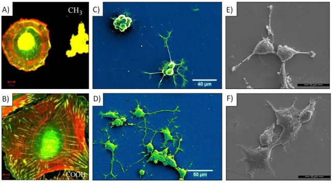
studies can be found in Figure studying both topography and surface functionalization. GaN provides
an example of the III-nitrides that has demonstrated a high degree of biocompatibility both as a
stand-alone surface and as one modified with biological molecules.3,93 GaN surfaces did not significantly affect or impede cell growth, and once etched showed a better cell adhesion than etched silicon.
Further work has been done on examining bare GaN surfaces with varied topographies and surface
adherence of cells.94 In general it has been shown that cells prefer rougher surfaces to smoother ones for adhesive ability.95 Mimicking surface roughness of tissue is possible using adlayers of polymer molecules, but similar effects have been shown using bare surfaces put through both etching and
polishing. One study in particular found that the effects of polishing and etching GaN were sufficient
to create a surface roughness suitable for cell growth and prorogation. This same study additionally
polishing. Subsequent increases were again observed with etching, and then finally sharply increasing
when nanowires were introduced. The cell phenotypes were dependent upon the surface of the GaN
following these treatments.2 Cells grew with significantly more branching when placed upon polished surfaces (high degree of parallel surface features) than the nanowire arrangement. These findings are
in agreement with research that examined modified-nanotextured GaN surfaces with similar values of
high cell adhesion capabilities for GaN.96 Both of these studies conclude that GaN is a suitable surface for biosensing uses and can be fabricated to encourage cell adhesion further. Surface
modification was used in both of these cases to create a more favorable surface for cell adhesion.
Figure 1.2. Cell growth on various GaN surfaces; A) and B) fibroblast growth on GaN using SAM
modified surfaces, adapted with permissions from Faucheux et al.1, C) and D) neuron growth on GaN
using modified surface topographies, adapted with permission from Bain et al.2, E) and F) neuron
cell growth using IKVAV binding proteins on GaN, adapted with permissions from Jewett et al.3
The inherent biocompatibility of other III-nitride materials is not as well understood or as
studied as GaN. What has been done however, does not yield as promising of results as modified GaN
surfaces. Research into AlN provided poor results which align with literature regarding aluminum
nitride’s toxic effects on different organ systems in mammals.92
cellular level studies along the AlN surface showed axonal degeneration and damage to glial cells
within a 10 day time frame.97 AlN is remarkably stable in biological media, but leeching of AlN occurs into solution and is dependent on the surface topography.92 Although damage may not be wide spread this would directly affect the stability of any cellular matrix that is being brought into contact
with an AlN device or sensor. Thus AlN seems a poor choice for biological sensing apparatuses.
A similar effect of AlN can be observed in AlxGa1-xN systems for biocompatible interfacing,
although to a lessened and more controllable degree. Examination of this effect revealed a relation
between cell death rate and increasing percent Al content within the AlxGa1-xN matrix. 98
In this work
Al content was measured from 0% up to 35% and throughout all examined concentrations of Al
within the AlxGa1-xN matrix there was evidence of cellular activity. 98
Growth rates of cells did
suffered with increasing Al, indicating that some of the toxic effects of AlN appear to carry over to
AlGaN. The conclusion to be drawn from this is that AlGaN (at least documented up to Al content of
35%) does not directly mirror pure AlN for its lack of biocompatibility. Instead, previous work by
Podolska et al. highlighted AlGaN as a promising surface for biological sensor interfacing as well,
although noted some cell counts were suboptimal.99 This also helps support the use of AlGaN/GaN type heterostructures for biosensing devices where cell interfacing or interactions may be a
possibility.
InN and InGaN have been shown in literature to have a similar behavior to AlN/AlGaN.
Regarding their cellular interfacing, some evidence suggests that the ternary InGaN may behave in
similar fashion to AlGaN as described.81 While InN has shown some promise as a biosensing platform fewer experiments have explored InN behavior with cellular structures. InN has been tested
in biological media for the stability of InN surfaces and surface components, but less focus on directly
binding cells for tissue interfaces. InN has similar behavior to AlN when placed in a biological system
malfunction.81 Thus interfacing directly with InN may be unfavorable for cellular systems. One study of InGaN however, revealed that theses surfaces may provide a biocompatible intermediate between
InN and GaN.100 Here, lymphocytes were grown on flexible LED devices including Si, AlInGaPAs, and InGaN. This may prove similar to AlGaN that when In is the lesser component of a GaN ternary
system the toxic effects can be mediated. In turn allowing for a biologically compatible surface to be
made from an In based III-nitride compound. Until this is done AlGaN/GaN and GaN systems will
likely remain the III-nitride of choice for biocompatible material systems.
1.6. Chemical functionalization
The surfaces of III-nitride materials have available bonding sites depending on the polarity of
the surface from its growth procedure.9 These dangling bonds are what give III-nitride materials their broad range of functionality for various analytes or chemical acceptors. Here we will cover some
III-nitride compounds and selected functionalization methods and schemes.
1.6.1. Aluminum nitride
The applications of AlN are more limited in biosensor applications due to concerns of
aluminum toxicity in biological environments. However, many chemical modification methods have
been explored to create a selectively sensitive surface upon AlN. One such surface modification with
broader application can be seen with a benzenethiosulfonate (BTS) crosslinker capped organosilane
coating.5 This work highlights the ability of organosilane adlayers to act as a platform for immobilization of relevant compounds such as biotinthiol. These organosilane surface coatings form
what is known as a self-assembled monolayer (SAM) and have been well documented as surface
for such organosilane SAMs typically require etchants such as H2SO4 or piranha to remove surface
contaminants and organics.1 Pentafluorophenyl ester and β-propiolactone were among several other chemical silanization methods studied alongside BTS, all of which serve to immobilize a specific
functional group onto the surface.102 Silanization of these surfaces has also been shown using dip coating techniques and subsequent heat treatments for adlayers of polysilazane to generate ceramic
coatings atop AlN.103 These techniques demonstrate the versatility of these surfaces under more precise surface bond modifications and using higher throughput processing techniques such as the dip
coat. For processing of AlN with silanization the surfaces are often terminated with hydroxyl groups
at available bonding sites. Exposure of surfaces after etching or during etching with an H2O2 solution
allows for hydroxylation to take place, thus making uniform SAM possible along AlN surfaces.7 This could eventually open up other chemical means of functionalization by immobilizing non SAM
molecules or compounds to these hydroxyl group sites.
1.6.2. Gallium Nitride
With regards to biosensing and functional surface regions, GaN has been more widely
researched and explored than AlN. As mentioned in the discussion of AlN, organosilanes and SAMs
play an important role in GaN chemical functionalization as well. The use of monolayers like
aminopropyltriethoxysilane (APTES) or thioglycolic acid (TGA) have been shown to successfully
immobilize surface biomolecules for sensing schemes.104,105,106 A schematic of some of the different chemical functionalization methods discussed here can be found in Figure .
Further work has been done into exploring chemical termination methods without the use of a
silane adlayer for GaN based sensors. Etching techniques on GaN surfaces can be done to terminate a
surface with hydroxyl groups, but with additional steps aid in incorporating another molecule onto
using a phosphoric acid and phosphonic acid mix to create ethephon binding sites for future
biomolecule attachment.21,61 Additional surface functionalization work via organophosphonic acids have been shown to be an alternative to common silanization methodology.108 Phosphonic acid functionalization methods do not rely on surface hydroxide group concentration, and can bind to both
oxide groups and hydrogen terminated sites.109 Thus functionalization of GaN surfaces using phosphonic acids as a vehicle for other biologically relevant groups is a viable option for future
surface modification schemes. As mentioned previously, phosphonic and phosphoric acids are
capable of etching III-nitrides where other more common etchants cannot. This slower etching
process creates new binding sites for other phosphonic acid derivatives to occupy as the etching takes
place.107
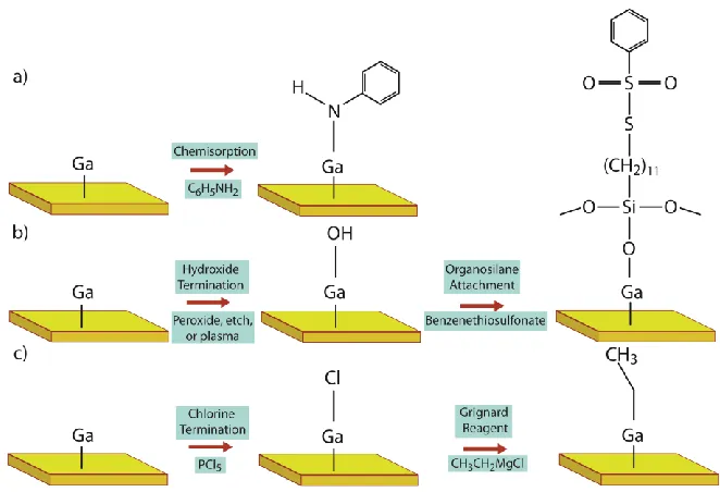
Figure 1.3. a) Basic chemisorption functionalization with analine following ion bombardment of GaN
surfaces under UHV conditions.4 b) Example of organosilane surface attachment following hydroxide termination to the surface, using the forementioned TUBTS molecule.5 c) Example of a Grignard
Other methods of binding 1-alkene groups to GaN surfaces have been explored to generate
similar layered structures to those seen by silanization and covalent attachment with phosphonic
groups. Photochemical assisted binding of alkenes has been performed using ultraviolet (UV) light at
a wavelength of 254 nm.110 Surfaces in this work were hydrogen terminated via inductively coupled hydrogen plasma and then exposed to 254 nm UV once placed in a solution of an alkene-amine
molecule (10-trifluoro-acetamide-1-decene, abbreviated TFAAD).110 This generates a highly stable surface but lacks the adaptability of phosphonic groups while adding a plasma treatment step.108 Additionally, UV treatments on biological molecules can lead to degradation of the newly bound
molecules or functional groups on the surface. Thermal methods of 1-alkene binding have thus been
explored to provide other options for this type of surface chemical functionalization. It was found that
heat treating surfaces coated in the same TFAAD solution at 180°C was successful in binding the
alkene group of the decene molecule to both hydroxyl groups and oxide groups on GaN surfaces.111 This shows the ability to attach 1-alkenes to GaN when UV degradation is a concern, and vice versa if
thermal degradation is an issue the UV method operates on the same chemical mechanism. Aside
from photopatterning and thermal treatments another method of 1-alkene surface termination to GaN
has been done using olefin metathesis. Here a first generation Grubbs catalyst (ruthenium chloride
complex) was used following alkene surface termination to create an olefin cross-metathesis reaction
to bind a 7-bromo-1-heptene marker to the GaN surface.6 Resultant surfaces proved resistant to oxidation and stable enough to move to attachment of a peptide monolayer to the GaN surfaces.112 Here a 6-heptenoic acid was bound to the alkene terminated surfaces using the same olefin metathesis
method. Peptide was successfully added to these alkene surfaces thus showing this scheme as a
Another method of wet chemical functionalization using the Grignard reaction has been
demonstrated for GaN surfaces. Grignard reagents in a broader sense are alkyl halides introduced to
magnesium in solution to generate a RMgX molecule, with R representing the alkyl group and X
representing the halide.113 This method is typically used for generating carbon-carbon bonding in organic molecules. However, here it was presented as a means to cap GaP, GaAs, and GaN surfaces
for superior surface stability in solution.114 The termination of the surface in alkyl chains prevented the degradation of GaN surface via oxidation and was able to maintain the electrical properties of the
GaN film. Few experiments have been done on this methodology in regard to other crystalline
III-nitride surfaces and their functionalization for biosensing or otherwise. Other work has been done
using the Grignard reagents as a step within a larger chemical functionalization method, but it was not
presented as the primary focus of the study itself.6 Thus, the full breadth of applications of Grignard reagents on III-nitrides is promising as more focus is given to these materials for tailorable
biofunctional surfaces. Additionally there are research opportunities in examining the Grignard
reactions on other III-nitride surfaces to explore their functionalization capabilities as well.
Earlier modification techniques utilized vacuum approaches to GaN functionalization and it is
worthy of discussion as these processes are still viable options. Chemical functionalization of GaN
under such conditions can be seen in the chemisorption of aniline and halogenated anilines under
pressures of approximately 5 × 10-11 Torr.4,115 Aniline and aniline compounds were introduced to GaN surfaces following ion bombardment to remove surface contaminants and vacate surface dangling
bonds. This method is successful for depositing high purity compounds onto the surface, but is not
suitable for compounds and biomolecules mentioned in the previous chemical functionalization
methods for GaN. Thus, research into high vacuum processing for GaN biosensors has not been fully
The departure from ultra-high vacuum processing for functionalization follows the trend for
GaN in that functionalization methods are become progressively more accessible to simpler bench top
chemistry procedures. Current methodology stated here has removed much of the time and resource
intensive processing and replaced it with schemes and techniques which allow for a wider range of
surface chemistries.
1.6.3. Aluminum gallium nitride (AlGaN)
As one of the most commonly used tertiary allows from the III-nitride set of materials,
AlGaN is used heavily in biosensing research. However, the functionalization of AlGaN is not well
explored as it is most commonly used in combination with GaN to form a heterojunction type device.
Under these circumstances surface functionalization is similar to GaN in its response to surface bond
termination schemes.
1.7. Sensing devices
Selectivity can be defined as a biosensor’s ability to ignore outside interference when taking a
measurement or registering an electrochemical interaction between surface bound receptors and
analytes present in solution.116 This interference can be noise or other processes that cause some minor or major surface charge changes to the biosensor. Specificity in similar fashion refers to the
actual ability of the biosensor to single out t.arget compounds, biomolecules or ions within
solution.117 One could view this as analyte bycatch, or unwanted entities occupying receptor sites and thus blocking possible interactions that would contribute to the biosensor’s total sensitivity. These
two things contribute to the overall sensitivity of the biosensor which represents the net output or
signal change that a sensor can detect. Higher sensitivity means that a device can detect lower
the signal that can be obtained. Research in the field has progressed towards a wider range of surface
modifications and improved III-nitride biosensor fabrication techniques enabling modern biosensors
to be tailored to a variety of testing modalities.
When operating a given biosensing modality the response of the material or device relative to
the environmental factors can be described as the sensing mechanism. In the design and use of
III-nitrides for sensing applications there are several different schemes which have been well established
in literature.118-122 Most research into III-nitride biosensors is done through microfabricated devices that are capable of being produced in large quantities. Sensors such as FETs and HEMTs rely on
conductance and charging effects to sense environmental stimuli.21 Others such as SAWS monitor physical motion of molecules and material and are a type of microelectromechanical system
(MEMS). Both of these types of sensors act as transducers for the external stimuli and the electrical
signal given off by the sensor and do so by taking advantage of the piezoelectric properties of
III-nitride materials. SAWS measure shifting piezoelectric properties for the III-III-nitride to generate an
output. FETs operate as a function of the interfacial conductance effects between their heterostructure
layers; examples include AlGaN and GaN or InGaN and GaN in terms of III-nitrides. The 2DEG
discussed earlier is an example of this induced channels at the hetero-interface between AlGaN and
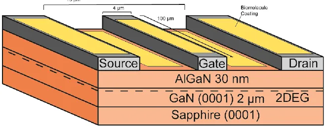
GaN.123 Along with the interface layer between the ternary and binary III-nitride two other interfaces are also present; the environment with the surface layer (in this case AlGaN in the AlGaN/GaN
system) and the interface of the lower layer with the substrate itself (in this case GaN). A schematic
of this device structure can be seen in Figure 1.4.124 Sensing along the surface interface relates the chemistry from the outer layer of AlGaN or GaN to the interior 2DEG and is what determines the
sensing capabilities for a biosensing device. When considering both the piezoelectric and spontaneous
polarization of the AlGaN and GaN they are often lumped together as a net polarization effect and are
GaN depend on the aluminum content in the AlGaN. The piezoelectric component of the polarization
is affected by strain induced by replacing Ga with Al and causes a mismatch at the lattice interface
with bulk GaN.126 When these properties are viewed as macroscopic polarization effects for each material they can be effectively seen as fixed surface charges.124 Since the surfaces of the GaN bulk layer are in contact with either the substrate or the AlGaN layer these will ideally remain unchanged
when put into operation. AlGaN however has an exposed surface to the environment and any internal
electric field caused by polarization is now subject to environmental interactions with the AlGaN
surface. Conductance and electrical behaviors will change within the 2DEG present along the
AlGaN/GaN interface relative to the effects that surface charging will have on the internal electric
field. Thus, monitoring the current flow or potential in AlGaN/GaN FETs becomes a means to
quantify environmental effects on the sensor itself. Additionally the interface structure of the
AlGaN/GaN devices is highly stable and allows for a high transconductance at low potentials and
often without the need for an external electrode.127 These surfaces are typically functionalized or capped with a receptor specific to a given environment or to an analyte intended to be measured.128 The focus here will be put upon FET type setups and gas sensors relative to III-nitrides. SAWs will
not be covered in this text; readers are encouraged to start with reviews and papers such as these.122,121
Figure 1.4. Schematic of biomolecule functionalized AlGaN/GaN FET. Adapted with the permission