Mobile Jammers in Educational Institutions
Dr. K.A.Lathief
Professor in the department of Electronics and Communication,
Jimma University, jimma Ethiopia.
Abstract
Mobile Jammer is a transmitter used to broadcast electromagnetic signals capable of blocking frequencies used by cellular/PCS systems. When active in a certain area, the mobile jammer will prevent any cellular/PCS system from communicating with the base station, and by this prohibiting all incoming and outgoing calls. Mobile Jammer have become a necessity for accomplishing a more cultured society because there is a growing demand for controlling the use of cellular phones in public places such as religious places, theaters, libraries, and others. The ‘GSM jammer’ focuses on cost, durability, and health issues. The max2364 chip was used as the cellular transmitter; thus, reducing the overall cost of the jammer system regarding the reduction of
electromagnetic radiation in the environment.
Keywords: Jammer/Disabler Technology
2.Introduction
Five types of devices are known to have been developed (or being considered for development) for preventing mobile phones’ communications in certain specified locations [1]:
A. Type ‘A’ Devices: ‘jammers’. It contains several independent oscillators transmitting jamming signals’ that block frequencies used by mobile communication devices for call establishment.
B.Type ‘B’ Devices: ‘intelligent cellular disablers’. The device normally works as a detector. When it detects signaling from
the Base station to the mobile station, it signals the base station not to establish communication. This process of detection and interruption of call establishment is done during the interval normally reserved for signaling and handshaking.
C. Type ‘C’ Devices: ‘intelligent beacon disablers’. These devices act as beacons’, i.e. they instruct any mobile device within their area of coverage to disable its ringer or disable its operation. The problem is that these types of devices require intelligent hadsets.
D. Type ‘D’ Devices: ‘Direct Receive and Transmit Jammers’. They behave as a small independent base station. The jammer is predominantly in receiving mode and will intelligently choose to interact and block the cell phone directly if it is within close proximity of the jammer.
E. Type ‘E’
Devices: ‘EMI Shield – Passive Jamming’. This technique uses Electro Magentic Interference (EMI) suppression techniques to construct what is called a Faraday cage. The Faraday cage essentially blocks, or greatly
2.1. Selective Frequency Jamming
A. DescriptionA ‘smart’ jamming approach would be to disturb the control process and thus prevent the establishment of a speech channel. This can be achieved by transmitting noise at the same frequency of the signal performing the control process. This method consists of detecting the frequency of the control process using the radio
frequency signal analyzer PXI 5660. The latter interfaces with a computer, providing it with a data file in which all detected frequencies and their corresponding power level are recorded. The frequency detection process consists of selecting the frequencies with a power level greater than 33.01 dBm [3].As a second step and after determining the frequency of the channel reserved for the control process; the system transmits noise at the detected frequency. Below is a block diagram representing the first approach.
B. Limitations
Although this alternative insures accurate jamming of the channel initiating a conversation, it wasn’t
implemented due to huge difference between the time needed to ensure successful frequency blocking and achievable time. The average read time in hard drives available is 8.9 ms and the average write time is 10.9 ms so the total time needed for analysis and detection of the frequency is more than 20 ms. On the other hand the time of one time slot (corresponding to one frequency hop) according to the GSM standard is
0.577ms.Note that this alternative could be implemented either if technologies yield faster hard drives (more than 200,000 RPM speed technologies) or if another method is implemented where the frequency detector directly delivers the frequency to the jammer transmitter.
2.2 Suggested ‘Smart’ Jammer Design
C. OverviewAs a last step in our research for an acceptable design, we decided to drop the selective frequency option, and based our attention on the power compensation issue of the mobile jammer. In this last design, we decided to broadcast a single low-bandwidth signal with a varying carrier that covers the whole uplink/downlink
bandwidth while restricting the jammer operation time.
D. Description
The improved jamming procedure is described as follows:
1. Construct a table indicating power levels at all channels of the GSM spectrum.
2. Detect an increase in the power level indicating control signals exchange between the mobile station and the base station indicating an eminent phone call or a location update.
3. Inform (trigger) the jammer circuit to begin operation.
6. Move the carrier through the whole uplink/downlink with a rate high enough to ensure that frequency hopping doesn’t allow the station to continue its signal exchange with the base station.
7. Stop operation when the time of operation exceeds a certain predefined value.
E. Implementation
a) The receiver subsystem
A receiver (possibly the NI PXI-5660 RF signal analyzer) is utilized for monitoring the GSM band in order to detect an increase of the power levels above 33 dBm, and then cause the sending of a control. This latter will be used either for turning on the whole transmitter circuit (mainly the max2364 IC), or for triggering an oscillator to generate the signal to be sent.
b) The max2364
The circuit design depends mainly on the max2364,which is a dual-band uadrature transmitter that is built by Maxim Company to function in cellular handsets. The output RF frequency is a function of the frequency supplied by a local oscillator. It is given by the relation :
where fREF is the frequency of the oscillator. RFM is the radio frequency main divider; RFR is the radio frequency reference divider, these two values are stored in local registers inside the chip.
c) Covering uplink/downlink
The noise signal with a low bandwidth is supplied to the IC, and for covering the whole range one of two
3. Options may be considered:
a) Supplying a constant fREF for the max2364 from a simple oscillator system, while continuously changing the contents of the RFM and RFR registers through a 3-wire control.
b) Keeping the values of the previously mentioned registers fixed, and supplying a continuously varying fREF through a circuit containing a voltage controlled oscillator (VCO) with a varactor, whose input voltage is a time varying periodic signal which increases/decreases in a manner such that the corresponding values of RF traverse the whole Uplink/Downlink range.
c) Stopping Transmission
In order to insure minimum power consumption and dissipation, while maintaining full efficiency of the scrambling system, the transmitter operation may be stopped after making sure that no speech channel establishment was possible.
4. Simulation
where :
• The repeating sequence block represents the periodic input signal to the VCO (more specifically the varying voltage at the pins of the variable capacitor) in the simulation it is considered to be a triangular signal buty any periodic signal would lead to the same results.The signal was given a triangular variation from 0 � 5v and a period of 0.2885 msec1.
• The VCO which represents the oscillator formed by the varactor and an inductor, the range to be traversed by fREF is 285.9 KHz which corresponds to a 5v variation in the input signal and thus a sensitivity of 57.11 KHz/volt. A
Discrete-time VCO was used to allow the use of the fast fourier transform to analyze the signal.
• The last part is the buffer and the FFT which help construct the frequency domain representation of the output signal achieved.
5. Results
On Running the simulation, and observing the output of the scope, a signal whose carrier repeatedly moves from 10.6927 to 10.9786 MHz is observed ( In fact, this is an FM signal with a varying carrier frequency).The output of this circuit is the input to pin#36 of the IC and we can see that the result is a signal at frequency RF which moves on the range of 935 � 960 MHz and thus covering the whole downlink.
Figure 2: Spectrum of the output signal
The circuit that uses a colpitt’s, and output a varying frequency oscillating signal was constructed and simulated using the Electronic workbench:
C6 is varied from 2 to 2.20891 pF to ensure the required frequency variation.
The circuit to control the operation time of the jammer using a 555 timer:
Figure 4 operation time controller of the jammer
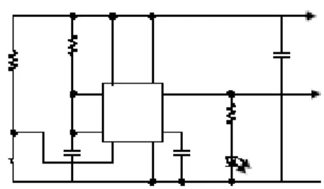
The Jammer has the following schematic:
where the circuits of figures 3 and 4 are connected to pins 36 and 27 respectively.
6. Conclusion
The increased need for mobile scramblers makes it vital that they integrate more features and provide more control on the whole process. This paper discusses mobile jamming technology, and introduces suggested improvements on existing designs. It presents possible approaches for a more intelligent design. The first approach (Selective Jamming) was not implemented due to hardware speed limitation, which may be overcome
with certain technologies. The proposed design achieves lower power consumption, taking into consideration health and cost issues.
References
*1+ Mobile & Personal Communications Committee of the Radio Advisory Board of Canada, “Use of jammer and disabler Devices for blocking PCS,Cellular & Related Services” availableat:
http://www.rabc.ottawa.on.ca/e/Files/01pub3.pdf
*2+ Sage, C., “Microwave and Radio Frequency Exposure: A Growing Environmental Health Crisis” available at:www.sfms.org/sfm/sfm301h.htm