ANALYSIS OF PLANAR MICROSTRIP CIRCUITS USING
THREE-DIMENSIONAL TRANSMISSION
LINE MATRIX METHOD
N. Komjani Barchloie and M. Solaimani
Department of Electrical Engineering, Iran University of Science and Technology Tehran, 16844, Iran, [email protected] - [email protected]
(Received: June 14, 2000 – Accepted in Revised Form: July 5, 2001)
Abstract The frequency-dependent characteristics of microstrip planar circuits have been previously analyzed using several full-wave approaches. All those methods directly give characteristic of the circuits frequency by frequency. Computation time becomes important if these planar circuits have to be studied over a very large bandwidth. The transmission line matrix (TLM) method presented in this paper is another independent approach for obtaining the frequency-domain results for microwave circuits through time-domain results, followed by Fourier transform. The advantage of this method is obtaining characteristics versus frequency over the whole band with a single simulation. The method is shown to be an efficient tool for modeling microstrip planar circuits as well as rectangular microstrip antennas and filters. The frequency characteristics calculated with the 3D-TLM method show excellent agreement with measured values and results obtained by other methods.
Key Words Planar Microstrip Circuit, TLM Method
ﻩﺪﻴﻜﭼ
ﻮﻳﻭﻭﺮﻜﻳﺎﻣﺢﻄﺴﻣﺕﺍﺭﺍﺪﻣﻲﺴﻧﺎﻛﺮﻓﻪﺼﺨﺸﻣﻥﺩﺭﻭﺁﺖﺳﺪﺑﻱﺍﺮﺑﻱﺩﺪﻌﺘﻣﺝﻮﻣﻡﺎﻤﺗﻞﻴﻠﺤﺗ ﻱﺎﻬﺷﻭﺭ
ﺩﺭﺍﺩ ﺩﻮﺟﻭ
. ﻢﻴﻫﺍﻮﺨﺑﺮﮔﺍ ﻭﺪﻨﻫﺩﻲﻣﺹﺎﺧ ﺲﻧﺎﻛﺮﻓﻚﻳﺭﺩ ﺍﺭﺕﺍﺭﺍﺪﻣ ﻲﺴﻧﺎﻛﺮﻓﻪﺼﺨﺸﻣ ﺎﻬﺷﻭﺭﻦﻳﺍ ﻲﻣﺎﻤﺗ
ﺑ ﺪﻳﺎﺑ ﺍﺭ ﻱﺯﺎﺳ ﻪﻴﺒﺷ ،ﻢﻳﺭﻭﺎﻴﺑ ﺖﺳﺪﺑ ﻊﻴﺳﻭ ﻲﺴﻧﺎﻛﺮﻓ ﺪﻧﺎﺑ ﻚﻳ ﺭﺩ ﺍﺭ ﺕﺍﺭﺍﺪﻣ ﻦﻳﺍ ﻪﺼﺨﺸﻣ
ﻚﺗ ﻚﺗ ﻱﺍﺮ
ﻲﻣﻲﻧﻻﻮﻃﻲﻠﻴﺧﻱﺯﺎﺳﻪﻴﺒﺷﻥﺎﻣﺯﻪﺠﻴﺘﻧﺭﺩ؛ﻢﻴﻨﻛﺭﺍﺮﻜﺗﺪﻧﺎﺑﻞﺧﺍﺩﻱﺎﻬﺴﻧﺎﻛﺮﻓ ﺩﺩﺮﮔ
. ﻲﻟﺎﻘﺘﻧﺍﻂﺧﺲﻳﺮﺗﺎﻣﺵﻭﺭ
ﺢﻄﺴﻣ ﺕﺍﺭﺍﺪﻣ ﻲﺴﻧﺎﻛﺮﻓ ﺦﺳﺎﭘ ﻥﺩﺭﻭﺁ ﺖﺳﺪﺑ ﻱﺍﺮﺑ ﺖﺳﺍ ﻱﺮﮕﻳﺩ ﻞﻘﺘﺴﻣ ﻩﻮﻴﺷ ،ﻪﻟﺎﻘﻣ ﻦﻳﺍ ﺭﺩ ﻩﺪﺷ ﻪﺋﺍﺭﺍ
ﻪﻳﺭﻮﻓ ﻱﺎﻬﻳﺮﺳ ﺯﺍﻩﺩﺎﻔﺘﺳﺍ ﺎﺑ ﺕﺍﺭﺍﺪﻣ ﻲﻧﺎﻣﺯﺦﺳﺎﭘ ﺯﺍ ﻮﻳﻭﻭﺮﻜﻳﺎﻣ
.
ﺯﺍ
ﻪﺼﺨﺸﻣ ﻥﺩﺭﻭﺁ ﺖﺳﺪﺑﺵﻭﺭﻦﻳﺍ ﻱﺎﻳﺍﺰﻣ
ﺖﺳﺍ ﻱﺯﺎﺳ ﻪﻴﺒﺷﻚﻳ ﺯﺍﻩﺩﺎﻔﺘﺳﺍ ﺎﺑﺎﻬﻨﺗ ﻲﺴﻧﺎﻛﺮﻓﺪﻧﺎﺑ ﻞﻛ ﺭﺩﺕﺍﺭﺍﺪﻣ ﻲﺴﻧﺎﻛﺮﻓ
. ﻩﺪﺷ ﻩﺩﺍﺩﻥﺎﺸﻧ ﻪﻟﺎﻘﻣ ﻦﻳﺍﺭﺩ
ﻱﺎﻫﺮﺘﻠﻴﻓ،ﻲﭙﻳﺮﺘﺳﺍﻭﺮﻜﻴﻣﻱﺎﻬﻨﺘﻧﺁﻞﻴﺒﻗﺯﺍﻮﻳﻭﻭﺮﻜﻳﺎﻣﺢﻄﺴﻣﺕﺍﺭﺍﺪﻣﻱﺯﺎﺴﻟﺪﻣﻭﻞﻴﻠﺤﺗﻱﺍﺮﺑﺵﻭﺭﻦﻳﺍﻪﻛﺖﺳﺍ
ﻭﻱﺭﻮﻧﻪﺒﺷ
...
ﺩﻮﺳﺭﺎﻴﺴﺑﺵﻭﺭ ﺖﺳﺍﻱﺪﻨﻣ
. ﺎﺑﻲﺑﻮﺧﻖﺑﺎﻄﺗﺵﻭﺭﻦﻳﺍﺯﺍﻩﺪﺷﻪﺒﺳﺎﺤﻣﻲﺴﻧﺎﻛﺮﻓﻱﺎﻫﻪﺼﺨﺸﻣ
ﺩﺭﺍﺩﺕﻻﺎﻘﻣﺮﮕﻳﺩﺯﺍﻩﺪﻣﺁﺖﺳﺪﺑﺞﻳﺎﺘﻧﻭﻩﺪﺷﻱﺮﻴﮔﻩﺯﺍﺪﻧﺍﺞﻳﺎﺘﻧ
.
1. INTRODUCTION
Up to 1985 mainly analysis techniques in the frequency-domain have been used for the design of planar microwave circuits. All those methods directly give characteristic of the circuits frequency by frequency, so computation time becomes important if these planar circuits have to be studies over a very large bandwidth. During the last decade, different time domain methods such as FD-TD and TLM have become very popular in the analysis of arbitrary microwave structures. The two major advantages of time
via Fourier transformation.
In this paper an overview shall be given on TLM simulations of electromagnetic fields and application of this method to planar microwave circuit design. It will be shown that this technique is a powerful analysis technique for microstrip planar circuits as well as microstrip antennas and filters. The frequency dependent scattering parameters have been calculated for several printed microstrip circuits, specifically for a line-fed rectangular patch antenna, a low-pass filter, and a side coupled band-pass filter. Good agreement between theory and measurement is obtained.
2. 3D-TLM ELECTROMAGNETIC MODELING
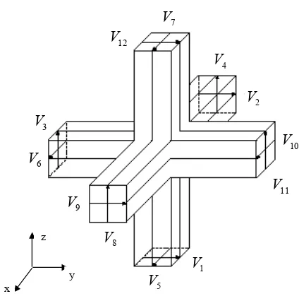
The symmetrical condensed node (SCN) TLM was used in this study. It is more powerful than other TLM nodes because the boundary description is easier, all six-field components can be defined at a single point in space, and there is less dispersion in axial directions. Figure 1 shows schematically the arrangement of the transmission line mesh in the 3 dimensional space. The ports 1-12 are associated with the so-called link line while the ports 13-18 are associated with stub-transmission lines. The role of these stub-transmission lines is two folds.
In the regular mesh they are used to model dielectric and magnetic properties of the transmission media. In the variable mesh approach they also add capacitance or inductance in order to assure time synchronism in the irregularly graded mesh. The TLM algorithm consists of the scattering process that can be described symbolically as:
n r n n i n n 1 n
i C .S .V C .V
V + = + (1)
Where Vin+1 is an incident voltage impulse at time step “n+1” and V is a reflected ri impulse, S is the TLM impulse scattering n
matrix and C is a connection matrix with n elements 1cij= , if port “i” is connected to port “j” and cij=0, otherwise. The size of the stub-loaded S-matrix is 18×18 [1,2].
In order to truncate problems, boundary conditions have to be established. Some boundary conditions that can be used in TLM simulation are electric and magnetic walls and absorbing boundaries. Electric and magnetic walls simulate terminated link-lines with reflection coefficient
1
L =
ρ and ρL =−1 respectively. The ABCs modeled by an impulse reflection coefficient are realized by terminating the link-line, of characteristic impedance ZL, with reflection coefficient ρL =(Zb−ZL)/(Zb+ZL) where Zb is the medium characteristic impedance. This technique works well at all frequencies for TEM waves. However, for dispersive structure such as microstrip, the termination is totally absorbing only at one frequency since the guide impedance is a function of frequency. Many other solutions have been proposed recently to improve the simulation of absorbing layers [3,4]. In this simulation, we used second order Higdon’s ABCs, which uses only the fields at the neighboring,
1
V
2
V
3
V
4
V
5
V
6
V
7
V
8
V
9
V
10
V
11
V
12
V
z
space and time nodes. The TLM voltage impulse incident on the absorbing boundary at the mth space step and the nth time step, n
m
V , can be expressed in terms of it’s immediate neighbors along the normal to the boundary as follows:
∑∑
= = − − = 2 0 i 2 0 j j n i m ij nm a V
V (2) Where
[ ]
γ
−
βγ
−
β
−
αγ
−
αβ
−
γ
β
α
α
=
p sp p sp sp s s p s ij0
a
and 2 1 s 2 1 s 2 1 sγ
+
γ
=
γ
β
+
β
=
β
α
+
α
=
α
2 1 p 2 1 p 2 1 pγ
γ
=
γ
β
β
=
β
α
α
=
α
2 1 2 1 sp 2 1 2 1 sp 2 1 2 1 sp α γ + γ α = αγ β γ + γ β = βγ α β + β α = αβ0
200
400
600
800
1000
1200
1400
1600
1800
2000
-4
-2
0
2
4
6
8
10
(a) (b)
(c)
(d)
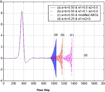
(a) a=b=0.50 & e1=0.0 e2=0.0
(b) a=b=0.50 & e1=0.1 e2=0.0
(c) a=b=0.50 & modified ABCs
(d) a=b=0.25 & e1=e2=0.
The interpolation coefficients αi,βiand γiare: l ∆ ε − − − − − − = γ i i i i a 1 ga(1 gbb)
l ∆ ε − − − − + − = β i i i i a 1 ag (11 gb)b
l ∆ ε − − − − − − = α i i i i a 1agg(1(1b)b)
Where
t c cos
g i
i= θ ∆∆l. The parameter gican also be written in terms of the effective dielectric constant of the guide and for the symmetrical condensed node gi =2 εeffi . The choice of the effective permittivity forces the ABCs to absorb incident waves with a limited range of propagation velocities.
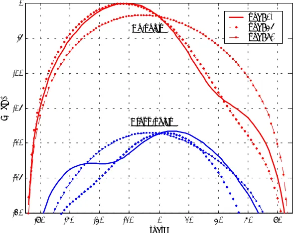
Figure 2 shows a propagating E pulse at z microstrip line on RT/duroid substrate of thickness 0.635mm and strip width 0.635mm. The effective dielectric constant of the substrate is 9.6. It is seen in Figure 2 that adding the damping factors (ε1,ε2) slows down the build-up of oscillations for the coefficients a=b=0.5. But for the coefficients a=b=0.25, it does not have any appreciable effect. Hence, we have used a=b=0.25 and ε1=0.1/∆l,ε2 =0. in our analysis and to avoid instabilities for boundaries placed 20 cells away from the circuit edges. In particular, the TLM method has the capability of impulse excitation and is stable under this condition. However the impulse excitation is avoided in practical structures for various reasons:
• Strong dispersion at high frequencies.
• Excitation of spurious modes in the TLM mesh. • Longer convergence time.
• The lack of high quality (broadband and stable) absorbing boundary conditions.
We have used a cosine-modulated Gaussian pulse to excite only the frequencies of interest. The time and frequency characteristics are given,
respectively, by: ) t t ( f 2 cos . e ) t (
V 2 0 0
) t t ( 2 2 0 − π = σ − − (3) Where σ is the standard deviation. The parameters of V(t), (σ,f0,t0) are such that the signal spectrum covers the antenna response. In order to satisfy causality, V(t) must be close to zero at t =0. In discrete form, V(t) can be written as:
t ) n n ( f 2 cos . e ) n (
V 2s 0 0
) n n ( 2 2 0 ∆ − π = − − (4) Where the standard deviation is given in terms of the time step, such that σ=s.∆t. The offset iterations are chosen so that the negative tail of the pulse is not significantly truncated. If the value of
) n (
V − 0 is to be 10−7, then n 5.7s
0≥ . The
standard deviation is chosen so that a significant signal injected at the highest frequency of interest and this signal falls off rapidly as the frequency is increased further. If the value of F(ω) at
max
f 2π =
ω is to be 10−7, then s≥3.7. For most of the work in this paper a standard deviation of
t
33∆ with an offset of 330 interactions were found to be convenient.
To compute the scattering parameters, we must compute the incident, and reflected current waves at the input (Iinc,Iref)and the transmitted current wave at the output port (Itran). By assuming that the tangential electric field is negligible at nodes adjacent to the strip conductor, the time domain current waves are defined as a loop integral of the magnetic field around the strip as:
∫
= H.dl ) t (I (5)
the computational domain, and compute the field of the transmitted waves Itran at the output port and total field Itot at the input port. The reflected field is obtained by subtracting the incident field from the total field (Iref =Itot −Iinc) [5]
) ( I ) ( Z ) ( I ) ( Z S S ) ( I ) ( I S ) ( I ) ( I S inc 1 1 o trans 2 2 o 12 21 inc 2 ref 2 22 inc 1 ref 1 11 ω ω ω ω − = = ω ω − = ω ω − = (6)
Where Zo1(ω) and Zo2(ω) are the characteristic impedances of the line connected to ports 1 and 2 respectively. )I(ω is the discrete Fourier transformed current given by:
) N / mn 2 j exp( ) t n ( i t ) f m ( I DFT 1 N 0 n DFT π − ∆ ∆ = ∆
∑
− = 1 N ,...., 2 , 1 , 0 m; = DFT − (7)
Where f∆ is the frequency resolution of the frequency domain calculation, m is the frequency index, t∆ is the sampling period of the DFT and
DFT
N is the length of the DFT summation ) t . f / 1 N
( DFT = ∆ ∆ .
Thus, the TLM method simulation is summarized as follows:
1) Filling computational space with SCN meshes. 2) Truncating the computational space with low reflection absorbing walls.
3) Placing structure in the computation volume. 4) Exciting the structure with Gaussian pulse whose width is chosen to cover the frequency bandwidth of interest.
5) Observing the transient waveform in the time-domain at a proper location.
6) Extracting the scattering parameter in the frequency domain by using Fourier transform.
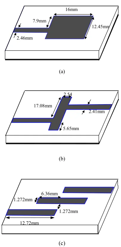
3. NUMERICAL RESULTS
Figure 3 shows a rectangular microstrip antenna and filter that have been measured [7,8] and analyzed by the three-dimensional FDTD method by the author’s [9]. The substrate thickness (h) and dielectric constant (εr), the space steps (∆x,∆y,∆z) and total mesh dimension (Nx,Ny,Nz)in the x, y, z direction and time step(∆t) used in simulation for this simulation are given in Table 1.
3-1. Line-Fed-Rectangular Microstrip
Antenna The edge-fed rectangular patch
antenna and actual dimensions is depicted in Figure 3a .In order to model the dimensions of the antenna and the substrate thickness correctly ∆x=0.400mm, mm∆y=0.389 andmm 265 . 0 z=
∆ have been chosen, thus the total mesh dimensions are 120×70×30 in the x, y and z directions, respectively. The rectangular antenna patch is 40∆x×32∆y. The length of the microstrip line from the source plane to the edge of the antenna is 60∆xand the reference plane for port 1 is 20∆xfrom the edge of the patch. The microstrip line width is 2.33mm and modeled with 6∆y. The time step used is
sec p 4295 . 0 t=
∆ . The simulation is performed for 10,000 time steps. The reflection coefficient results, shown in Figure 4, show good agreement with the measured data [7]. The calculated first and second resonance are alternately 7.54 GHz and 18.22 GHz, while the measured values are 7.6GHz and 18.37GHz. Thus, good agreement obtained between operating resonance and
TABLE 1. Substrate Characteristic And Mesh Dimension For Structures Shown In Figure 3.
Geometry h(mm)
ε
r∆
x
∆
y
∆
z
Nx Ny Nz∆
t
1 0.794 2.20 0.400 0.389 0.265 120 80 30 0.4295
2 0.794 2.20 0.423 0.406 0.198 86 86 20 0.3143
experiment.
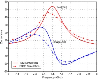
The input impedance of the antenna may be calculated from the S11calculation by transforming the reference plane to the edge of the microstrip antenna. Figure 5 shows the input impedance calculation near the operating resonance, compared with FDTD simulation. [9] Figure 6 shows the electrical surface current distribution on the patch and feedline at 7.5GHz. It illustrates that the microstrip line feeds at the no radiating edge. The x directed current is dominant by the current on the feedline.
the two principal plane axis and diagonal plane at 7.5GHz is plotted in Figure 7. Because the feedline and the radiating patch are on one surface, the spurious radiation from the feed degrades the side lobe levels or increase cross-polarized radiation.
3-2. Microstrip Low-Pass Filter The low
pass filter analyzed is shown in Figure 3b. The space steps used are ∆x=0.4233mm,mm
y=0.4064
∆ and ∆z =0.1985mm and the total mesh dimension are 86×86×20 in the x, y and z direction, respectively. The long rectangular patch is thus 6∆x×50∆y. The distance from the source plane to the edge of the long patch is 50∆x, and the reference planes for port 1 and 2 are 20∆x
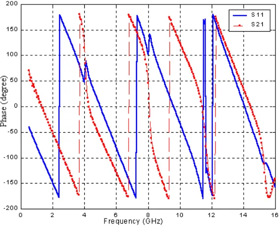
from the edges of the patch. The strip widths of the ports 1 and 2 are modeled as 6∆x. The time step used is ∆t=0.3143psec. The simulation is performed for 10000 time steps. The scattering coefficient results - shown in Figures 8 and 9 - and again good agreement is obtained.
3-3. Side-Coupled Microstrip Line The
configuration of the analyzed microstrip line is shown in Figure 3c. The net size of the equivalent circuit used here ismm z
y
x=∆ =∆ =0.212
∆ . The space steps used
are ∆t=0.353psec, and the total mesh dimension are 120×60×20 in the x, y and z direction, respectively. The scattering parameters calculated are shown in Figures 10 and 11 compared with measurement [10]. The computed results show excellent agreement with the measured data.
4. CONCLUSION
The TLM method has been used to perform time domain simulations of pulse propagation in several printed microstrip circuits. In addition to the transient results, frequency-dependent scattering parameters and input impedance of rectangular patch antenna have been calculated by Fourier transform of the time-domain results. The characteristics were computed and excellent
16mm 7.9mm
12.45mm 2.46mm
(a)
2.54 17.08mm
2.41mm
5.65mm
(b)
6.36mm 1.272mm
1.272mm 12.72mm
(c)
5. REFERENCE
1. Komjani Barchloie, N., “Analysis of Passive and Active
Microstrip Antennas Using 3D-TLM Method”, Ph.D. Thesis, Iran University of Science and Technology, (July 2000).
Figure 4. Input reflection coefficient of the rectangular antenna shown in Figure 3a.
Figure 5. Input impedance of the rectangular antenna at 7.5GHz.
2 4 6 8 10 12 14 16 18 20
-30 -25 -20 -15 -10 -5 0
Frequency (GHz)
M
agni
tude S
11 (
dB
)
TLM simulation Measurement[7]
7 7.1 7.2 7.3 7.4 7.5 7.6 7.7 7.8 7.9 8
-30 -20 -10 0 10 20 30 40 50 60
Frequency (GHz)
Zi
n
(ohm
s)
TLM Simulation FDTD Simulation
Real(Zin)
2. Johns, P. B., “A Symmetrical Condensed Node for the Vol. MTT-35, No. 4, (April 1987), 370-377.
Figure 6. Current distribution of the aperture coupled patch antennaat 7.5GHz. (a) x-directed current and (b) y-directed current.
Figure 7. Radiation pattern of the aperture coupled patch antenna at 7.5GHz.
-80 -60 -40 -20 0 20 40 60 80
-30 -25 -20 -15 -10 -5 0
theta
E (
dB)
phe=0. phe=45 phe=90 Co-polar
Absorbing Boundary Conditions for 3D-TLM Analysis Planar and Quasi-Planar Structures”, IEEE Trans. Microwave
Theory Tech., Vol. MTT-42, No.9, (September 1994),
1669-1677.
4. Eswarappa, C. and Hoefer, W. J. R., “Absorbing Boundary Conditions for Time Domain TLM and FDTD Analysis of Electromagnetic Structures”, Electromagnetics, Vol. 16, (1996), 489-519.
5. Dhouib, A., Stubbs, M. G., Lecours, M., “Experimental and Numerical Analysis of a Microstrip/Stripline-Coupling Scheme for Multilayer Planar Antennas”, IEEE AP-S, (1994), 782-784.
6. Zhang, X. and Mel, K., “Time-domain Finite Difference Approach to The Calculation of The Frequency Dependent Characteristics of Microstrip Discontinuities”,
IEEE Trans. Microwave Theory Tech., Vol. MTT-36,
Figure 8. Magnitude scattering parameters of the low-pass filtershown in Figure 3b.
Figure 9. Phase scattering parameters of the low-pass filter shown in Figure 3b.
0 2 4 6 8 10 12 14 16 18
-40 -30 -20 -10 0
Frequency (GHz)
M
a
gn
it
ud
e S
11
(d
B
)
TLM simulation measurement [9]
0 2 4 6 8 10 12 14 16 18
-50 -40 -30 -20 -10 0
Frequency (GHz)
M
a
gn
it
ud
e S
21
(d
B
)
TLM simulation measurement [9]
0 2 4 6 8 10 12 14 16
-200 -150 -100 -50 0 50 100 150 200
Frequency (GHz)
P
ha
se
(d
eg
re
e)
No. 12, (September 1988), 1775-1787.
7. Chang, S., Nicolaos, W., Fordham, O., “Feeding Structure Contribution to Radiation by Patch Antennas with Rectangular Boundaries”, IEEE Trans. Antenna and
Prop. ,Vol. 40, No. 10, (1992), 1245-1249.
8. Dinzeo, G., Giannini, F., Sorrentino, R., “Novel Microwave Integrated Low-Pass Filters”, Elect. Letters.,, (1979), 136-138.
the Three-Dimensional Finite-Difference Time-Domain Method to The Analysis of Planar Microstrip Circuits”,
IEEE Trans. Microwave Theory Tech., Vol. MTT-38,
No.7, (July. 1990), 849-857.
10. Shibata, T., Hayashi, T. and Kimura, T., “Analysis of Microstrip Circuits Using Three Dimensional Full Wave Electromagnetic Field Analysis in The Time Domain”,
IEEE Trans. Microwave Theory Tech., Vol. MTT-36,
Figure 10. Magnitude scattering parameters of the band-pass filter shown in Figure 3c.