An Efficient Parallel Prefix Adder for Reverse Converter Design
Athira T G
1IES College of Engineering, Thrissur, Kerala, India Department of ECE
Sindhu T V
2IES College of Engineering, Thrissur, Kerala, India Assistant Professor, Department of ECE
I.
INTRODUCTION
In the world of battery-based and portable devices, the residue number system (RNS) can play a significant role due to its low power features and competitive delay. The RNS can provide carry free and fully parallel arithmetic operations for several applications, including digital signal processing and cryptography. However, its real usage requires forward and reverse converters to be integrated in the existing digital systems. The reverse conversion, i.e., residue to binary conversion, is a hard and time-consuming operation. Hence, the problem of designing high-performance reverse converters has motivated continuous research using two main approaches to improve the performance of the converters: 1) investigate new algorithms and novel arithmetic formulations to achieve simplified conversion formulas and 2) introduce new moduli sets, which can lead to more simple formulations. Thereafter, given the final simplified conversion equations, they are computed using well-known adder architectures, such as carry-save adders (CSAs) and ripple-carry architectures, to implement carry-propagate adders (CPAs) and, more seldomly, fast and expensive adders such as the ones with carry-look ahead or parallel prefix architectures.
1. Parallel prefix structure
The Residue number system mainly composed of three main parts such as, forward converter, modulo arithmetic units and reverse converter. On comparing with the other parts the reverse converter design is a complex and non modular structure. So more attention is needed in designing the reverse converter thereby preventing the slow operation and compromise the benefits of the RNS. The parallel prefix structure helps to achieve the faster operation in the reverse converter design but causes increased power consumption. In the existing system the novel specific hybrid parallel prefix adder based components are used to replace the existing components thereby reducing the power consumption and getting faster operation.
Abstract:
The implementation of residue number system reverse converters based on wellknown regular and modular parallel prefix adders is analyzed. The VLSI implementation results show a significant delay reduction and at the cost of higher power consumption, which is the main reason preventing the use of parallel-prefix adders to achieve high-speed reverse converters in nowadays systems. Hence to solve the high power consumption problem, novel specific hybrid parallel-prefix-based adder components that provide better trade off between delay and power consumption are herein presented to design reverse converters using the BK structure. Then modified using the Han carlson structure for better performance. A methodology is also described to design reverse converters based on different kinds of prefix adders. This methodology helps the designer to adjust the performance of the reverse converter based on the target application and existing constraintsFig.1 Basic parallel prefix structure
The Parallel prefix structure consists of three main blocks, they are preprocessing block, prefix carry tree and post processing block. The parallel prefix adder operation begins with preprocessing stage by generating the Generate (Gi) and Propogate (Pi) equation [1] & [3]. The prefix carry tree get proceeded with the previous block signal to yield all carry bit signal and these stage contains three logic complex cells such as Black cell, Gray cell and Buffer cell. Black cell compute both the propogate (P(i,j)) and generate (G(i,j)) by using the equation[3] &[4].The Gray cell executes only the generate(G(i,j)).The carry bits generated in the second stage get passed to the post processing block thereby generating the sum using the equation[5].The block diagram is shown in the fig.1
= AND (1) = (2)
= XOR (3) Po=0 (4)
:k OR :k AND :n (5) :k AND 6) = XOR (7)
The Brent Kung adder prefix structure is employed to achieve the higher speed with reduced power consumption. On comparing with the other parallel prefix adder structure the BK adder is chosen mainly for minimum fan out and should be higher speed in operation than others.
2. Hmpe structure
depends upon the initial inputs. Parallel: involves the execution of an operation in parallel. This is done by segmentation into smaller pieces that are computed in parallel. 7 Operation: any arbitrary operator that is associative is parallelizable. It is very fast because the processing is accomplished in a parallel fashion. In brief, the use of modular and regular parallel-prefix adders proposed in this brief in reverse converters highly decrease the delay at the expense of significantly more power and circuit area, whereas the proposed prefix-based adder components allows one to achieve suitable tradeoffs between speed and cost by choosing the right adders for the parts of the circuits that can benefit from them the most.
Fig.2 HMPE structure
Assuming the addition of A= a0, a1...an with B = b0, b1...bn the carry generate term gi, the carry propagate term pi = ai + bi, which can also be defined as pi = hi = ai © bi, where © denotes the exclusive-OR operation. The sum is given by S = A©B.
The basic cells used for the parallel prefix operations in these projects are as shown in the above fig.4 If high speed is the designer goal, the CPAs with EAC and the regular CPAs should be replaced by traditional parallel prefix modulo 2n – 1 adder and regular parallel-prefix adders, respectively. However, for the VLSI designers, a suitable tradeoff between speed, power, and area is often more important. a regular parallel-prefix adder with the desirable prefix structure can be used to perform the first part of the addition, for which the corresponding bits of the operands are fully variable, and a RCA with simplified logic to do the second part (full adder becomes XNOR/OR gates because of the constant operand). The proposed hybrid regular parallel-prefix XOR/OR (HRPX) adder component to perform the (4n + 1)-bit addition. It should be noticed that due to the architecture of the reverse converter, the carry output of the XNOR/OR chain is not needed and can be ignored as shown in Fig.5
Fig.4 logic level implementation of cells
3. Han-carlson structure
The HMPE is highly flexible, since it can be used with every prefix networks. Hence, the circuit performance metrics such as area, delay, and power-consumption can be adjusted by selecting the desired prefix structure. On the other hand, the HRPX avoids the usage of a large size parallel-prefix adder with high power consumption, and also does not have the penalty of using the long carry-propagation chain of a RCA.
The pre-processing and post-processing stages of a prefix adder involve only simple operations on signals local to each bit position. Therefore, adder performance mainly depends on prefix-processing stage. Fig.6 shows Han-Carlson prefix adders topologies. Here black dots represent the prefix operator while white dots are simple placeholders. Kogge-Stone adder is composed by levels and present a fan out of two at each level using a large number of black cells and many wire tracks. A good trade-off between fan out, number of logic levels and number of black cells is given by Han-Carlson. The Han-Carlson adder in Fig.6 uses a single Brent-Kung level at the beginning and at the end of the graph, and the number of levels is 1+
Fig.6 Han-carlson structure
II.
RESULTS
AND
DISCUSSION
In my project parallel prefix adder for reverse converter design is proposed. the proposed system can be used to generate the modulo addition of two numbers. It is the reverse converter section of the residue number system. The proposed system can be divided into two sections. The first section consists of the parallel prefix structure using BK structure. In the second section BK structure is replaced by the Han carlson structure. HMPE structure is used in the parallel prefix adder.
1. BK structure
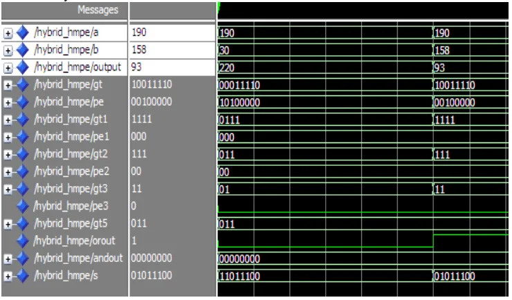
In the BK structure simulation having two inputs and is of 8 bit each and represented by a and b and the output is having the same. the output is generated by adding a and b numbers and getting their sum and check the modulo condition. it the sum is less than 255 same value displyed and if greater modulo 255 will taken.
2. Han-carlson structure
Second section is the modification of the parallel prefix BK structure is replaced by the Han carlson strcuture. Han carlson structure is having more efficient than the BK structure and having the less power consumption and delay.
Fig.8 output of the Han Carlson
3. Power and Delay analysis
The power summary of proposed system and modified system were found. In proposed system total power consumption is 93mW. There is a large number logic gates is reqiured in the BK structure of parallel prefix adder and more power is needed. In modified system, the power is reduced to 89mW.Using the Han carlson structure arrangement, number of logic gates reduced hence power decreased. In the proposed system combinational path delay is 19.244ns.Combinational path delay of modified system is 18.025ns and this is due to the Han carlson arrangement to the proposed structure.
Table 1 Comparison of proposed and modified systems
Proposed System Modified System
Power 93mW 89mW
Delay 19.244ns 18.025ns
III.
CONCLUSION
methodology the proposed components can be used in any reverse converter design with different moduli sets. The proposed HMPE structure is highly flexible; it can be replaced with Han carlson parallel prefix components that enhance the performance and also reduce the power and delay variations.
REFERENCES
[1]. Omondi and B. Premkumar, (2007)., Residue Number Systems: Theory and Implementations. London, U.K.: Imperial College Press
[2]. J. Chen and J. Hu, . (2013) “Energy-efficient digital signal processing via voltage over scaling-based residue number system,” IEEE Trans. Very Large scale Integr. (VLSI) Syst., vol. 21, no. 7, pp. 1322– 1332.
[3]. H. Vun, A. B. Premkumar, and W. Zhang, (2013) “A new RNS based DA approach for inner product computation,” IEEE Trans. Circuits Syst. I, Reg. Papers, vol. 60, no. 8, pp. 2139–2152.
[4]. S. Molahosseini, S. Sorouri, and A. A. E. Zarandi, (2012) “Research challenges in next-generation residue number system architectures,” in Proc. IEEE Int. Conf. Comput. Sci. Educ pp. 1658–1661. [5]. Y. Wang, X. Song, M. Aboulhamid, and H. Shen, (2002) “Adder based residue to binary numbers
converters for (2n − 1, 2n, 2n + 1),” IEEE Trans.Signal Process., vol. 50, no. 7, pp. 1772–1779,. [6]. S. Molahosseini and K. Navi,(2010) “A reverse converter for the enhanced moduli set {2n − 1, 2n + 1,
22n, 22n+1 − 1} using CRT and MRC,” inProc. IEEE Comput. Soc. Annu. Symp. VLSI, pp. 456–457. [7]. L. Sousa and S. Antao, , (2012)“MRC-based RNS reverse converters for the fourmoduli sets {2n + 1,
2n − 1, 2n, 22n+1 − 1} and {2n+ 1, 2n − 1, 22n, 22n+1 − 1},” IEEE Trans. Circuits Syst. II, vol. 59, no. 4, pp. 244–248.
[8]. L. Sousa and S. Antão, (2013). “On the design of RNS reverse converters for the fourmoduli set {2n +1, 2n −1, 2n, 2n+1+1},” IEEE Trans. Very Large Scale Integr. (VLSI) Syst., vol. 21, no. 10, pp. 1945–1949