Int. J. Nanosci. Nanotechnol., Vol. 15, No. 4, Dec. 2019, pp. 239-248
Imprecise Minority-Based Full Adder for
Approximate Computing Using CNFETs
Narges Hajizadeh Bastani1,* and Keivan Navi2
1
Department of Computer Engineering, Yadegar -e- Imam Khomeini (RAH) Branch, Islamic Azad University, 1815163111, Tehran, Iran.
2
Faculty of Computer Science and Engineering, Shahid Beheshti University, G.C., Evin 1983963113, Tehran, Iran.
(*) Narges Hajizadeh Bastani: [email protected]
(Received: 12 October 2018 and Accepted: 28 July 2019)
Abstract
Nowadays, the portable multimedia electronic devices, which employ signal-processing modules, require power aware structures more than ever. For the applications associating with human senses, approximate arithmetic circuits can be considered to improve performance and power efficiency. On the other hand, scaling has led to some limitations in performance of nanoscale circuits. Accordingly, Carbon Nanotube Field Effect Transistors have gotten a widespread attention as the most appropriate replacement for MOSFETs. In this paper, an imprecise full adder cell based on CNFET minority gates is introduced. Evaluation and comparison of the minority-based and the-state-of-the-art imprecise full adders in terms of average power dissipation, delay and power delay product (PDP) are done. The error distance (ED), normalized error distance (NED) and PDP-NED product metrics are also considered for assessing the accuracy of the reviewed circuits. The HSPICE simulations, conducted using Stanford 32nm CNFET model, indicate that the minority-based design outperforms the other designs in terms of performance and error tolerance.
Keywords:Approximate computing, Full adder, CNFET, Nanoelectronics.
1. INRODUCTION
In the recent years, the energy efficiency has become a paramount concern in design of computing systems as they become increasingly embedded and mobile.
Computational functions of today’s digital systems involve an expanded set of applications that encompasses media processes such as audio, video, and image processing. The limited perceptual capability of humans in construing images and videos, allows the outputs of media processing algorithms to be numerically approximate in preference to be accurate. Arithmetic units as a main infrastructure of media processor can be developed imprecise and provide further power saving compared to the conventional low-power design methodologies. Reducing area and delay in media processing systems is additional achievements of applying the approximation approaches.
N-type and P-type transistors, which have led to comparable designing techniques with CMOS technology. In addition, CNFETs have a near-ideal combination of a high-mobility and ultra-thin body channel [9, 10, 11, 12, 13, 14 and 15]. The I-V characteristics for a bulk nMOS and an N-type CNFET with same gate widths at 32 nm technology node are illustrated in Figure 1. The results indicate that the CNFET device shows less short channel effects, has higher driving current and transconductance (gm), and experiences less mobility degradation.
The threshold voltage of a CNFET can be determined by adopting the proper diameter for its CNTs as shown in Equation (1). The diameter of CNT is a function of the chirality vector, which defined by (n1, n2) indices, and the relation is given by the Equation (2) [9].
0.436
( )
CNT
th
V
D nm
(1)
2 2
1 2 1 2
0.0783 CNT
D n n n n (2)
Figure 1. The I-V characteristics of a 32nm MOSFET-like N-type CNFET (L=32nm, W=64nm (Tube=16, Pitch=4nm), (n1,n2)=(19,0)) vs. a 32nm NMOS (L=32nm, W=64nm) (a) Id-Vds (b) Id-Vgs (c) gm-Vgs [16].
The rest of the paper is organized as follows: in Section 2, the existing imprecise full adders are reviewed. In Section 3, the minority-based approximate full adder is described. The simulation results and comparisons are given in Section 4. Section 5 investigates an image processing application for imprecise full adder and finally Section 6 concludes the paper.
2. THE EXISTING APPROXIMATE FULL ADDERS
In this section, the state-of-the-art imprecise full adder cells are reviewed [2, 3, 4]. It is worth mentioning that the previous MOSFET-based designs have been modified and optimized for 32nm CNFET technology.
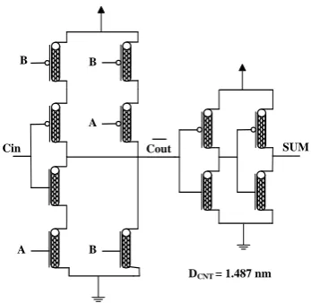
The first imprecise FA (IFA1) is an approximation structure of conventional CMOS mirror adder as shown in Figure 2.
Cout
DCNT = 1.487 nm Cin
A B
B A B
Cin
SUM Cin
Cin
B A
A B
Figure 2. Imprecise full adder 1 (IFA1)
full adder cell. There is one error in Cout and two errors in SUM in IFA1.
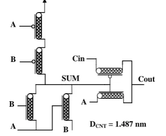
The second imprecise full adder (IFA2) is shown in Figure 3. Structure of IFA2 is based on the fact that SUM is inverse of Cout signal in six out of eight cases. SUM has only two errors, while Cout is correct for all combinations of input signals.
Cin A
A
A
A
Cout
B B
B B
SUM
DCNT = 1.487 nm
Figure 3. Imprecise full adder 2 (IFA2).
By combining IFA1 and IFA2, more transistors can be eliminated from the conventional design, which is resulted in imprecise FA3 (IFA3). This structure has one error in Cout and three errors in SUM. Figure 4 depicts the schematic of IFA3.
B
Cin
A
B
A
B
SUM Cout
DCNT = 1.487 nm
Figure 4. Imprecise full adder 3 (IFA3).
The truth table of the exact FA shows that the Cout signal is equal to the A signal and also equal to the B signal for six out of eight terms. Therefore, in imprecise FA4
(IFA4), Cout is considered as A due to the interchange relation between A and B signals. This design utilized an inverter to calculateCout, and SUM signal generates from Cout similar to IFA1. This structure has two errors in Cout and three errors in SUM. Figure 5 is illustrated IFA4.
Cout
DCNT = 1.487 nm
Cin
SUM Cin
Cin
B A
A B
A
Figure 5. Imprecise full adder 4 (IFA4).
The imprecise 8-transistor XNOR-based FA5 (IFA5), which is shown in Figure 6, is designed based on 10-transistor full adder in [17]. SUM signal of an accurate FA, is equal to Cin signal in half of the input signals combinations, so the functions of SUM and Cout are considered as Equations (3) and (4), respectively. In IFA5, both SUM and Cout are correct for four out of the total input combinations.
I
SUM Cout
Cout A
Cin
B A
DCNT = 1.487 nm
DCNT = 0.861 nm
DCNT = 0.861 nm
Figure 6. Imprecise full adder 5 (IFA5).
in
( )
out in
C AB C AB (4)
Imprecise FA6 (IFA6) with six transistors is approximate structure of accurate design in [18], which its functions of SUM and Cout are given by Equations (5) and (6) respectively:
SUM A B (5)
( )
out in
C AB C AB (6)
SUM signal is accurate for half of the eight input combinations, while Cout is accurate. The schematic of IFA6 in Figure 7 expresses that this circuit has four fewer transistors as compared to the accurate one.
A
B
A
Cin
A
Cout
B
B SUM
DCNT = 1.487 nm
Figure 7. Imprecise full adder 6 (IFA6).
Imprecise XNOR-based FA7 (IFA7), shown in Figure 8, is an extension of IFA6, with two more pass transistors to improve the accuracy of SUM signal. In this structure, SUM has only two errors, while Cout is accurate for all the possible combinations. The functions of SUM and Cout signals are as Equations (7) and (8), respectively:
( ) in
SUM AB C (7)
( )
out in
C AB C AB (8)
The other imprecise full adder (IFA8) based on CNFET is proposed in [4]. That proposal is designed based on NAND and NOR structure with 12 transistor.
SUM signal is accurate for six of the eight input combinations, while Cout is accurate.
Functions of SUM and Cout are given by Equations (9) and (10) respectively:
SUM A B C.( . )A B C.( ) (9)
Cout SUM (10)
An imprecise full adder cell has also been suggested in [19]. However, in this cell the Cout output is not full-swing and it has 0V and VDD/3 as ‘0’ and 2VDD/3 and VDD as ‘1’. As a result, this cell requires additional gate to complete the voltage level of the Cout signal and is suitable for blocks such as serial adders. Moreover, in this work important applications of imprecise adders such as image processing have not been investigated.
A
B
B
A B
A Cin Cin
SUM
Cout
DCNT = 1.487 nm
Figure 8. Imprecise full adder 7 (IFA7).
3. THE MINORITY-BASED APPROXIMATE FULL ADDER
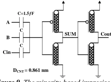
is 0v (all inputs are low) or 0.3v (only one of the input signals is high) according to the Voltage Transfer Characteristic (VTC) of the inverter, the output of the minority gate is high (VOH=0.9v). For other input combinations, divided voltage in the gate of the inverter is equal to 0.6v (two out of three input signals is high) or 0.9v (all of the input signals are high) and in keeping with VTC of the inverter, the output of the minority gate is low (VOL=0v).
A
B
Cin
SUM Cout
DCNT = 0.861 nm
C=1.5ƒF
C
C
Figure 9. The minority-based imprecise FA.
The small gate capacitance of the CNFET-based inverter is ignorable as compared to the input capacitors and does not affect the voltage level of the inverter’s input [21, 22]. It is notable that the utilized CNFET model in [21, 22] considers the gate and parasitic capacitances for simulations. It is also worth mentioning that implementing capacitors using CNFET transistors has been reported in [23]. Moreover, designing circuits based on capacitors and CNFETs has already been reported in [24]. It is worth mentioning that, in the CNFET technology wire capacitance can be reduced by replacing Cu interconnect with CNT bundle interconnect, and it is possible to obtain low voltage swing driving a wire with a capacitor [23].
Figure 10 demonstrates the voltage transfer characteristic (VTC) of the CNFET inverter. As compared to the 32nm MOSFET, 32nm CNFET has a quite sharper curve in the transition region due to the higher gain, which contributes considerable improvement in Noise
Margin [25]. This considerably sharp transition region is due to the very high intrinsic voltage gain of the CNFET inverter. As illustrate in Figure 1, CNFET has considerably higher gm and small signal resistance at the saturation region (ro) and consequently very higher intrinsic gain as compared to MOSFET. Nanoscale MOSFETs suffers from severe short channel effects, degraded mobility and velocity saturation, which degrade the intrinsic gain. The aforementioned benefits of CNFET make it more suitable for being utilized in minority structures.
The minority-based imprecise FA follows a similar logic with IFA2, which is expressed before. However, in the minority-based imprecise structure, a minority gate replaces the SUM generator circuit of IFA2 structure as depicted in Figure 9. Therefore, the two-transistor path for charge and discharge of the SUM node is decreased to one transistor. On the other hand, the branches on the SUM node in the minority-based imprecise FA are less than IFA2, which leads to lower power dissipation and delay. To generate the exact Cout function of the minority-based imprecise FA, an inverter is placed after SUM. In this structure, SUM has only two errors, while Cout is accurate for all input combinations.
Figure 10. The VTC of CNFET Inverter (DCNT=0.861 nm).
4. SIMULATION RESULTS
Stanford HSPICE Model for 32nm CNFET technology [21, 22]. This standard model for enhancement-mode MOSFET-like CNFET considers a pragmatic and circuit-compatible device structure for HSPICE simulations. This model includes realistic device nonidealities and parasitics such as inter-CNT charge screening effects, quantum confinement effects on both circumferential and axial directions, Schottky-barrier effects at contacts, finite scattering mean free path, doped source/drain regions and parasitic capacitance and resistance. Furthermore, it
considers a full transcapacitance network for more precise transient performance simulations with HSPICE. This CNFET model has already been widely used for simulation of different types of CNFET-based circuits in many valid references such as [9, 11, 12, 13, 14, 15, 16, 27 and 28].
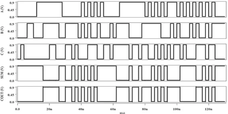
The transient response of the minority-based IFA, considering all 64 possible input transitions, is demonstrated in Figure 11, which indicates the correct and proper operation of this design.
Figure 11. Transient response of the minority-based IFA.
Some precision evaluation metrics such as Error Distance (ED), Mean Error Distance (MED) and Normalized Error Distance (NED) that introduced in [29] are used to evaluate approximate designs. Error distance (ED) is defined as the arithmetic distance between an erroneous output and the precise one. Total error distance (TED) is the sum the EDs for all the inputs of each full adder cell. The mean value of the EDs of all possible outputs is MED (Equation (11)), that is useful in evaluating the efficiency of an approximate implementation. Normalized error distance, referred to as NED, is used in characterizing the reliability of an approximate design (Equation (12)).
i i
i
MED
ED p (11)MED NED
D
(12)
wherepithe probability of ith input, and D is the maximum amount of error that an imprecise adder can take. In addition, the PDP-NED product is reported to investigate the power and precision tradeoff of approximate designs.
design has significantly lower PDP-NED product that specifies the efficacy of this design in trading off the accuracy for power. Since all previous designs were simulated with CNFET, Superiority of the proposed design is due to the approximate computing.
For the sake of completeness, the performance of the proposed imprecise full adder is also compared with accurate adder cell [30]. This is simulated under the same conditions described before. The comparisons are shown in Table 2, where the superiorities of the proposed imprecise design are clearly visible in terms of power and PDP.
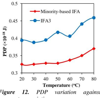
To evaluate the sensitivity of the circuits to the temperature variation, the temperature varied from 0 to 90 ˚C for proposed design and the IFA3 that had the best PDP compared to other designs. The
results for PDP are shown in Figures 12. As it can be seen PDP of the proposed circuit, are less affected by temperature variations as compared to the other design.
Figure 12. PDP variation against temperature variations.
Table 1. Performance comparison of the imprecise full adder cells.
IFA cells Power (nW) Delay (ps) PDP (aJ) TED NED PDP × NED
IFA1 76 7.86 0.597 2 0.083 0.050
IFA2 72.7 7.29 0.531 2 0.083 0.044
IFA3 59.1 6.68 0.395 3 0.125 0.049
IFA4 76.4 6.55 0.500 3 0.125 0.062
IFA5 219 80.4 17.6 4 0.166 2.921
IFA6 20.4 30.3 0.618 4 0.166 0.103
IFA7 28.4 76.2 2.16 2 0.083 0.179
IFA8 250.3 6.57 1.65 2 0.083 0.137
Minority-based IFA 16.1 20.4 0.329 2 0.083 0.027
Table 2. Simulation results (proposed versus exact full adders).
Design Power (nW) Delay (ps) PDP (aJ)
Exact FA 3148.4 6.73 21.2
Minority-based IFA 16.1 20.4 0.329
5. APPLICATION
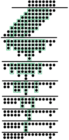
In this section, the application of the imprecise full adders is investigated in image multiplication. Partial products in multiplication are reduced with IFA cells and then these imprecise multipliers are compared with exact multiplier, which is reduced using exact full adder cells.
RGB (Red Green Blue) pixel values are numbers between [0, 255], so 8 bits are required for displaying each pixel; therefore 8×8 multiplication is performed for this application. It is worth noting that the image multiplying is performed using C++ language simulated in Microsoft Visual Studio 2012.
0.3 0.35 0.4 0.45 0.5
20 30 40 50 60 70 80
P
DP
(
×
10
-18
J)
The result of a pixel-by-pixel multiplication is an image that each RGB value of its pixels is obtained by multiplying two input images, and then the reduction stage is done using the imprecise and exact full adders. Figure 13 illustrates a 8×8 multiplier, where the partial products that are produced in the first stage multiplications, are reduced using full adder cells. In fact, in this type of multiplication, the full adders are cascaded in some levels, videlicet; the outputs of the full adders are used as the inputs of the next level full adders.
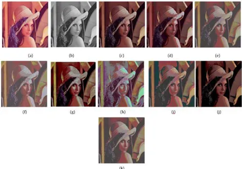
To identify the quality of the output image of the imprecise multiplier based on the minority-based imprecise FA and compare it with the output images of other imprecise and exact multiplier, the peak signal-to-noise ratio (PSNR) are measured and illustrated in Table 3.
Table 3. PSNR result of two image multiply examples.
Image processing results PSNR IFA1 (28.38, 29.34, 29.28) IFA2 (23.18, 20.31, 21.66) IFA3 (19.62, 18.23, 19.10) IFA4 (25.35, 23.68, 24.49) IFA5 (20.26, 19.35, 18.52) IFA6 (23.30, 22.11, 23.40) IFA7 (21.95, 25.13, 24.44)
Minority-based IFA (23.18, 20.31, 21.66)
PSNR measures the quality of the inexact output compared to the output of an exact multiplying.
For each example, PSNR values are represented with a three-valued vector that each index determines the PSNR of one of the RGB colors. According to Table 3 and the results of the image multiplying shown in Figure 14, the output image of the minority-based inexact multiplying has an acceptable quality as compared to the other inexact multiplying results. Moreover, as shown before in Table 1, it consumes considerably lower power. As a result, the
minority-based imprecise cell can be used in image processing applications to reach an efficient design.
6. CONCLUSION
A minority-based imprecise full adder with a simple circuit structure has been investigated in this paper. The simulations have been carried out using 32nm CNFET HSPICE model to evaluate the average power, delay and power delay product (PDP). The total error distance, normalized error distance and PDP-NED product metrics are also deliberated for evaluating the reliability of reviewed circuits. The application of these imprecise full adders in image processing is investigated and the PSNR of the output images is reported to determine the quality of the images. The minority-based full adder is superior in terms of performance, accuracy and error tolerance as compared to other modern imprecise FAs, recently introduced in the literature.
ACKNOWLEDGEMENT
I would like to express my deep gratitude to Dr. Mohammad Hossein Moaiyeri, for
his patient guidance, enthusiastic encouragement and useful critiques of this research work.
REFERENCES
1. Han, J., Orshansky, M., (2013). “Approximate computing: An emerging paradigm for energy-efficient design”, 18th IEEE European Test Symposium (ETS), 1-6.
2. Gupta, V., Mohapatra, D., Raghunathan, A., Roy, K., (2013). “Low-power digital signal processing using approximate adders”, Computer-Aided Design of Integrated Circuits and Systems, IEEE Transactions on, 32(1): 124-137.
3. Yang, Z., Jain, A., Liang, J., Han, J., Lombardi, F., (2013). “Approximate xor/xnor-based adders for inexact computing”, In IEEE International Conference on Nanotechnology.
4. Safaei Mehrabani, Y., Faghih Mirzaee, R., Zareei, Z., Daryabari, S. M., (2017). “A Novel High-Speed, Low-Power CNTFET-Based Inexact Full Adder Cell for Image Processing Application of Motion Detector”, Journal of Circuits, Systems, and Computers, 26(5): 1750082.
5. Moaiyeri, M. H., Sabetzadeh, F., Angizi, S., (2018). “An Efficient Majority-Based Compressor for Approximate Computing In The Nano Era”, Microsystem Technologies, 24(3): 1589-1601.
6. Shirinabadi Farahani, S., Reshadinezhad, M. R., (2018). “A new Twelve-transistor Approximate 4: 2 Compressor in CNTFET Technology”, International Journal of Electronics, 106(5): 1-16.
7. Roy, K., Mukhopadhyay, S., Meimand-Mehmoodi, H., (2003). “Leakage current mechanisms and leakage reduction techniques in deep-submicron CMOS circuits”, Proceedings of the IEEE, 91(2): 305-327.
8. Peng, L. M., Zhang, Z., Wang, S., (2014). “Carbon nanotube electronics: recent advances”, Materials Today, 17(9): 433-442.
9. Lin, S., Kim, Y. -B., Lombardi, F., (2011). ”CNFET-based design of ternary logic gates and arithmetic circuits”, IEEE Transactions on Nanotechnology, 10(2): 217-225.
10. You, K., Kundan, N., (2011). “Design of a ternary static memory cell using carbon nanotube-based transistors”, Micro & Nano Letters, 6(6): 381-385.
11. Rezaei Khezeli, M., Moaiyeri, M. H., Jalali, A., (2017). “Analysis of Crosstalk Effects for Multiwalled Carbon Nanotube Bundle Interconnects in Ternary Logic and Comparison with Cu interconnects”, IEEE Transactions on Nanotechnology, 16(1): 107-117.
12. Moaiyeri, M. H., Mehdizadeh Taheri, Z., Rezaei Khezeli, M., Jalali, A., (2018). “Efficient Passive Shielding of MWCNT Interconnects to Reduce Crosstalk Effects in Multiple-Valued Logic Circuits”, IEEE Transactions on Electromagnetic Compatibility, 1-9.
13. Moghaddam, M., Moaiyeri, M. H., Eshghi, M., (2017). “Design and Evaluation of an Efficient Schmitt Trigger-based Hardened Latch in CNTFET Technology”, IEEE Transactions on Device and Materials Reliability, 17(1): 267-277.
14. Marani, R., Perri, A. G., (2018). “Dynamic Simulation of CNTFET-Based Digital Circuits”, International Journal of Nanoscience and Nanotechnology, 14(4): 277-288.
15. Daliri, S. S., Javidan, J., Bozorgmehr, A., (2017). “Reducing Hardware Complexity of Wallace Multiplier Using High Order Compressors Based on CNTFET”, International Journal of Nanoscience and Nanotechnology, 13(1): 59-67.
16. Moaiyeri, M. H., Chavoshisani, R., Jalali, A., Navi, K., Hashemipour, O., (2016). “Efficient radix-r adders for nanoelectronics”, International Journal of Electronics, 103(2): 281-296.
17. Mahmoud, H. A., Bayoumi, M. A., (1999). “A 10-transistor low-power high-speed full adder cell”, Proceedings of the 1999 IEEE International Symposium on Circuits and Systems, 1: 43-46.
18. Lin, J. -F, Hwang, Y. -T., Sheu, M. -H., Ho, C. -C., (2007). “A novel high-speed and energy efficient 10-transistor full adder design”, Circuits and Systems I: Regular Papers, IEEE Transactions on, 54(5): 1050-1059.
19. Pounaki, N., Moaiyeri, M. H., Navi, K., Bagherzadeh, N., (2015). “An Ultra-efficient Imprecise Adder for Approximate Computing Based on CNTFET”, The CSI Journal of Computer Science and Engineering, 13(1): 31-37.
20. Navi, K., Moaiyeri, M. H., Mirzaee, R. F., Hashemipour, O., Mazloom Nezhad, B., (2009). “Two new low-power full adders based on majority-not gates”, Microelectronics Journal, 40(1): 126-130.
21. Deng, J., Wong, H. S., (2007). “A compact SPICE model for carbon-nanotube field-effect transistors including nonidealities and its application—Part I: Model of the intrinsic channel region”, IEEE Transactions on Electron Devices, 54(12): 3186-3194.
22. Deng, J., Wong, H. S., (2007). “A compact SPICE model for carbon-nanotube field-effect transistors including nonidealities and its application—Part II: Full device model and circuit performance benchmarking”, IEEE Transactions on Electron Devices, 54(12): 3195-3205.
23. Kim, Y. –B, Kim, Y. –B., (2010). “High Speed and Low Power Transceiver Design with CNFET and CNT Bundle Interconnect”, Proc IEEE International SOC Conference, 152-157.
24. Reshadinezhad, M. R., Moaiyeri, M. H., Navi, K., (2012). “An Energy-Efficient Full Adder Cell Using CNFET Technology”, IEICE Transactions on Electronics, E95.C(4): 744-751.
25. Cho, G., Kim, Y. B., Lombardi, F., Choi, M., (2009). “Performance evaluation of CNFET-based logic gates”, In Instrumentation and Measurement Technology Conference, 909-912.
26. Nayeri, M., Keshavarzian, P., Nayeri, M., (2019). “A Novel Design of Quaternary Inverter Gate Based on GNRFET”, International Journal of Nanoscience and Nanotechnology, 15(3): 211-217.
27. Liang, J., Chen, L., Han, J., Lombardi, F., (2014). “Design and evaluation of multiple valued logic gates using pseudo N-Type carbon nanotube FETs”, IEEE Transactions on Nanotechnology, 13 (4): 695–708. 28. Lin, S., Kim, Y. B., Lombardi, F., (2012). “Design of a ternary memory cell using CNTFETs”, IEEE
Transactions on Nanotechnology, 11(5): 1019-1025.
29. Liang, J., Han, J., Lombardi, F., (2013). “New Metrics for the Reliability of Approximate and Probabilistic Adders”, in Computers, IEEE Transactions on, 62(9): 1760-1771.