FPGA Implementation and Design of Low Power
Sequential Filter
Shivam Singh Sikarwar Deepak Sharma
M. Tech Student Assistant Professor
Department of Electronics and Communication Engineering Department of Electronics and Communication Engineering Lord Krishna College of Technology Indore (M.P), India Lord Krishna College of Technology Indore (M.P), India
Abstract
We will present the design and FPGA implementation of sequential digital 8-tap FIR filter using a novel micro programmed controller based design approach. In this paper, the FIR filter is designed for operation controls by micro programmed controller. The proposed FIR filter will be coded in VHDL using modular design approach, and implement in Spartan-3E FPGA. The performance evaluation and synthesis results obtained through Xilinx ISE synthesis tool and functionally checked in Model sim module.
Keywords: FIR Filter, Implementation of FIR Filter, Micro Programmed Controller
________________________________________________________________________________________________________
I.
I
NTRODUCTIONDigital finite impulse response (FIR) filters are the basic building block of many digital signal processing (DSP) systems. FIR filters are used due to their stability and linear phase properties. The main objectives of digital FIR filter are to filter out undesirable parts of the signal, shape the spectrum of signals in communication channels, signal detection or analysis in radar applications. Adders, multipliers and delay elements are the main component used in the implementation of digital FIR filters. These components are arranged and interconnected in different ways based on the architecture of the FIR filter.
Filter Classification: A.
The digital filter can be broken into three categories: time domain, frequency domain and custom. As previously described, time domain filters are used when the information is encoded in sin waveform. Time domain filtering is used for such actions as: smoothing, DC removal, waveform shaping, etc. In contrast, frequency domain filters are used when the information is contained in the amplitude, frequency, and phase of the component sinusoids. The goal of these filters is to separate one band of frequencies from another. Custom filters are used when a special action is required by the filter, something more elaborate than the four basic responses (high-pass, low-pass, band-pass and band-reject). For instance, describes how custom filters can be used for deconvolution, a way of counteracting an unwanted convolution.
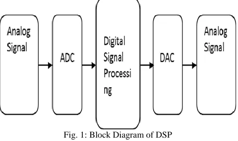
Fig. 1: Block Diagram of DSP
Digital finite impulse response (FIR) filters are the basic building block of many digital signal processing (DSP) systems. FIR Filters are used due to their stability and linear phase properties. The main works of digital FIR filters are to filter out undesirable parts of the signal shape the spectrum of signals in communication channels, signal detection or analysis in radar applications. Adders, multipliers and delay elements are the main components used in the implementation of digital FIR filters. These components are arranged and interconnected in different ways based on the architecture of the FIR filter.
( ) ∑ ( ) ( )
II.
P
ROPOSE METHOD FORFIR
FILTERFir filter is implemented using shift and add method. We perform all out optimization in the multiplier block. The constant multiplications are decomposed in to additions and shifts and the multiplication complexity is reduced. It’s possible to implement the design in the two form described below.
1) The coefficients are changed to integer getting multiplied to a multiple power of 10, and then we arrange these coefficients positive power of n.
2) First arrange decimal coefficients according to negative and positive power of 2 (no need to them into integer). So the filter hardware and power consumption will reduce.
III.
C
OMPARISON BETWEENA
NALOG FILTER AND DIGITAL FILTERTable – 1
Digital filters Analog filters
High accuracy Less accuracy due to component tolerances Linear phase (FIR filters) Non-linear phase
No drift due to component variations Drift due to component variations Flexible, adaptive filtering possible Adaptive filters difficult
Easy to simulate and design Difficult to simulate and design Computation must be completed in sampling
period – limits real time operation
Analog filters required at high frequencies and for anti-aliasing filters Requires high performance ADC, DAC and
DSP No ADC, DAC or DSP required
IV.
FIR
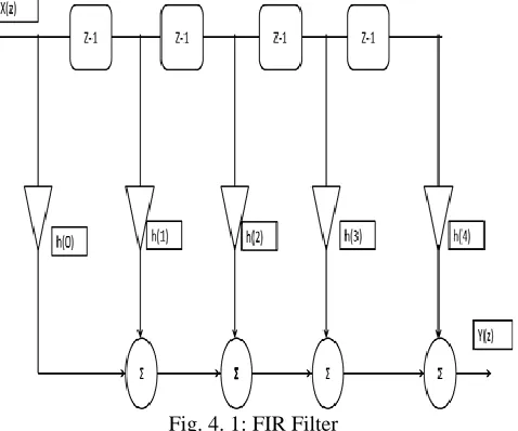
FILTERA filter (Finite input response filter) is a digital filter that is widely used in digital signal processing applications. The FIR-filter calculates an output from setof input-samples. The set of N input samples is multiplied by a set of coefficients and then added together to produce the output ¾ see Fig. 4.1. The filter behavior is determined by the filter-coefficients. A general FIR filter is described inthe following equation:
( ) ( ) ( ) ( ) ( )
Where ki is the coefficient i. x is the input signal and y isthe output signal. m is the number of filter coefficients ¾called taps, and n is the input sample number.
Implementation of FIR-filters can be undertaken in either software or hardware. A software implementation will require sequential execution of the filter-functions. Hardware design of FIR-filters allows the filter functions to be executed in a parallel manner which make sim proved filter processing speed possible.
V.
I
MPLEMENTATION OF FIR FILTERConvolution is the mathematical process that relates the output, y(t), of a linear, time-invariant system to its input, x(t), and impulse response, h(t). That is,
( ) ( ) ( ) ( ) ( ) (1)
Where "*" represents the commutative convolution operation. The continuous time relationship is described by the familiar convolution integral.
( ) ∫ ( ) ( ) (2)
For infinite discrete sequences, designated by x(n), y(n), and h(n), this integral relation reduces to another familiar expression, the convolution sum.
( ) ∑ ( ) ( ) (3)
For two finite discrete sequences of length Nx and Nh, the linear or aperiodic convolution sum takes on a slightly different form.
( ) ∑ ( ) ( ) (4)
Where h(k) and x(n-k) are zero outside their appropriately defined intervals. For Nx > Nh, each summation need only be calculated for the 0 £ k £ Nh-1 terms. The output, y(n), will have length Nx+Nh-1.
Convolution processing is notoriously computationally intensive. Direct application of Equation 4 in a tapped delay line architecture requires on the order of 2× Nh2operations (Nh multiplications and additions for each output sample) to produce an output Nh samples long. For typical audio signals, a three second impulse response sampled at 44.1 kHz requires around 2× (3× 44,100)2 or 35 billion computations to convolve with the same length input.
Processing in the frequency domain introduces significant input to output latency, since the input must be initially buffered and transformed into the frequency domain. Conversely, the output must be inversely transformed into the time domain. The buffering imposes minimum 2 × Nx sample latency. The frequency transformation itself and the convolution process introduce further overhead
Other convolution methods aim to reduce the number of required computations and reduce the amount of input to output latency without altering the expected output. Some of these techniques include block convolution and hybrid time/frequency processing.
Fig. 5.11: Illustrates The Data Path Architecture Of FIR Filter.
VI.
M
ICRO PROGRAMMED CONTROLLERbased on load enable (LE) signal. Once loading the input data in the first register, the input data is multiplied and accumulated based on the select signals (S1 and S0), product select (Ps) and load accumulator (lacc) signals.
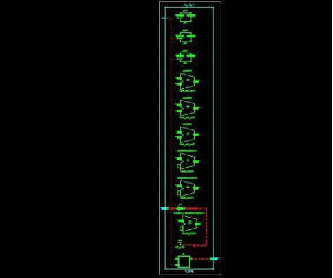
Fig. 6.1: Architecture of FIR Filter
VII.
A
PPLICATIONSDigital FM Stereo A.
A digital FM stereo decoder uses the phase characteristics of linear phase FIR filters, together with a mathematical operation, to generate a 38 kHz subcarrier signal from a 19 kHz pilot. The subcarrier signal is mixed with the input composite signal from which the pilot has been removed to shift its L-R component to baseband; the linear phase FIR filters also maintain phase coherence between the subcarrier and the composite signals.
SONAR B.
Different digital filters used in sonar signal processors perform two major functions, the filtering of waveforms to modify the frequency content and the smoothing of waveforms to reduce the effects of noise.
RADAR C.
Digital processing has also permitted increased capability for extracting target information from the radar signal. SAR provides an image of a scene. Radars are used to recognize one type of target from another, with the help of digital processing,
VIII.
A
DVANTAGE1) They can have exactly linear phase. 2) They are always stable.
3) The design methods are generally linear. 4) They can be realized efficiently in hardware. 5) The filter startup transients have finite duration.
IX.
R
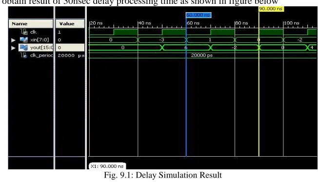
ESULTIn simulation result we obtain result of 30nsec delay processing time as shown in figure below
Fig. 9.1: Delay Simulation Result
Accordingly to our result shown in figure 9.2 power consumption of designed circuit is around 18mw which is less than 50 mw as compared to previous work.
X.
F
UTURE SCOPEThe present work on the new multiplier architecture can be further extended in various directions. The design can be simulated to check the power consumption. Other methods can be implementing with this to further improve the delay. In order to carry out complete analyze, the circuit can be extended to chip level where the delays due to wiring, PAD and interconnects are included.
XI.
C
ONCLUSIONSFrom above result we can conclude that the propose method provide delay less than Array Multiplier and consume more time to perform same task using Vedic Multiplier, Carry Look Ahead Adder and Ripple Carry Adder method. Power consumption calculation result in figure 9.2 shows that power get reduce by 50mW using proposed method.
R
EFERENCE[1] S. A. Khan, Digital Design of Signal Processing Systems: A practical approach, John Wiley and Sons, United Kingdom, 2011. [2] U. Meyer-Baese, G. Botella, D. E. T. Romero and Martin Kumm, “Optimization of high speed pipelining
[3] Y. Zhou and P. Shi, “Distributed Arithmetic for FIR Filter implementation on FPGA,” Proc. of IEEE Intl. Conf. on Multimedia Technology (ICMT’2011), Hangzhou, China, pp. 294-297, July 2011.
[4] F. Nekoei, Y. S. Kavian and O. Strobel, “Some schemes of realization digital FIR filters on FPGA for communication applications,” Proc. Of 20th Intl. Crimean Conference on Microwave and Telecommunication Technology (CriMiCo’2010), Crimea, Ukraine, pp.616-619, Sept. 2010.
[5] B. W. Bomar, “Implementation of microprogrammed control in FPGAs,” IEEE Transaction on Industrial Electronics, Vol. 49, No. 2, pp. 415-422, Apr. 2002.
[6] Barkalov and L. Titarenko, Logic synthesis for Compositonal Microprogram Control Units, Springer, Berlin: Germany, 2008.
[7] R. Wiśniewski, A. Barkalov, L. Titarenko and W. Halang, “Design of microprogrammed controllers to be implemented in FPGAs,” Intl.Journal of Applied Mathematics and Computer Science, Vol. 21, No. 2, pp. 401-412, June 2011.
[8] RUPALI MADHUKAR NARSALE and DHANASHRI GAWALI, “DESIGN & IMPLEMENTATION OF LOW POWER FIR FILTER: A REVIEW”,
International Journal of VLSI and Embedded Systems-IJVES, Vol 04, Issue 02; March -April 2013