POLY(3-METHYLTHIOPHENE) BRUSHES: STRUCTURE, MORPHOLOGY, AND ELECTRONIC TRANSPORT
Mark Moog
A dissertation submitted to the faculty at the University of North Carolina at Chapel Hill in partial fulfillment of the requirements for the degree of Doctor of Philosophy in the
Department of Physics.
Chapel Hill 2018
Approved by: Frank Tsui
Wei You... Sean Washburn
c 2018 Mark Moog
ABSTRACT
Mark Moog: POLY(3-METHYLTHIOPHENE) BRUSHES: Structure, Morphology, and Electronic Transport
(Under the direction of Frank Tsui)
Low charge carrier mobility is a major obstacle that limits the performance of organic electronic devices. For conjugated polymers, increasing the contribution from intramolecular charge transport channels to overall charge transport is expected to increase the mobility of the overall device. This is because the transport of charge carriers along conjugated polymer backbones is expected to be much faster than transport between the polymers. However, de-signing devices that take advantage of intramolecular charge transport has proven difficult, and in virtually all organic electronic devices charge must travel not only along individ-ual polymer backbones, but must hop inefficiently between polymers as well due to film morphology.
Conjugated polymer brushes are films comprising densely packed conjugated polymers that are tethered to a substrate, causing the polymers to elongate creating a brush-like mor-phology. Due to their morphology, polymer brush devices are expected to exhibit enhanced intramolecular charge transport. Electronic devices can be made from polymer brush films by growing the polymer from a conducting substrate and attaching a metal electrode to the top of the brush film, forming the vertical electrode-polymer-electrode structure. These devices make it possible to investigate intramolecular charge transport processes, because each polymer which contacts the top electrode is also contacting the bottom electrode (i.e. the substrate).
envi-ronmental and thermal stability. In this work the morphology and electronic properties of poly(3-methylthiophene) (P3MT) brushes are studied using the vertical electrode-polymer-electrode devices. The bulk resistivity of P3MT brush devices was found to be 1.4⇤105⌦-cm,
ACKNOWLEDGMENTS
TABLE OF CONTENTS
LIST OF TABLES . . . ix
LIST OF FIGURES . . . x
LIST OF ABBREVIATIONS AND SYMBOLS . . . xiii
1 INTRODUCTION . . . 1
1.1 Review of Essential Chemistry . . . 2
1.1.1 Molecular Orbitals and Conjugation . . . 2
1.1.2 Polymers . . . 3
1.1.3 Organic Semiconductors . . . 4
1.2 Organic Electronics . . . 10
1.2.1 A Brief History and Overview of Organic Electronics . . . 10
1.2.2 Charge Transport and Mobility in Organic Semiconductors . . . 11
1.2.3 Metal - Organic Semiconductor Interfaces . . . 17
1.3 Molecular Electronics . . . 23
1.3.1 A Brief History and Overview of Molecular Electronics . . . 23
1.3.2 Charge Transport in Molecular Wires: From Tunneling to Hopping . 25 1.4 Polymer Brushes . . . 28
2.1 P3MT Brush Synthesis and Device Fabrication . . . 29
2.1.1 Experimental Procedure . . . 33
2.2 Bulk Structure Measurements . . . 35
2.2.1 Cyclic Voltammetry . . . 35
2.2.2 Rutherford Backscattering Spectroscopy . . . 37
2.2.3 Grazing Incidence Wide Angle X-ray Scattering (GIWAXS) . . . 40
2.3 Surface Morphology . . . 40
2.3.1 Atomic Force Microscopy (AFM) and Scanning Electron Microscopy (SEM) Imaging . . . 40
2.3.2 Height-Height Correlation Function . . . 42
2.4 Electronic Measurements . . . 43
2.4.1 Conductive AFM (cAFM) Measurements. . . 43
3 P3MT BRUSH STRUCTURE AND MORPHOLOGY . . . 44
3.1 Bulk Measurements . . . 44
3.1.1 Brush Density . . . 44
3.1.2 Polymer Chain Orientation within the Brush . . . 50
3.2 P3MT Brush Surface Morphology . . . 53
3.2.1 Analysis of Surface Structure by AFM and SEM . . . 53
3.2.2 Quantifying Brush Thickness . . . 53
3.2.3 Column Analysis . . . 61
3.3 Summary . . . 74
4.1 Characterization of Charge Transport through CPB Devices. . . 76
4.2 I-V Behaviors . . . 100
4.2.1 Polymer-Electrode Contact Analysis for CPB Devices . . . 101
4.2.2 Bulk Resistivity and Molecular Resistivity for P3MT CPBs . . . 108
4.3 I-V Behavior as Finite Bias . . . 110
4.3.1 Energy Level Structure of CPB Devices . . . 110
4.3.2 The Injection Limited Current Model . . . 113
4.4 Summary . . . 118
5 CONCLUSIONS . . . 119
Appendix A COLUMN IDENTIFICATION ALGORITHM . . . 121
Appendix B I-V ADAPTATION OF THE ILC MODEL . . . 124
BIBLIOGRAPHY . . . 126 APPENDIX A: COLUMN IDENTIFICATION ALGORITHM
LIST OF TABLES
1.1 Conductivities of select materials . . . 5
1.2 Mobilities of select materials . . . 12
3.1 Representative height-height correlation function results for P3MT CPB films. 73 3.2 Monomer volume density extracted from various measurements. . . 74
4.1 Comparison of nominal film thickness (L0) and device thickness (d) . . . 107
4.2 Zero-field contact factor for KTP devices on CPB films . . . 108
LIST OF FIGURES
1.1 Benzene ⇡ delocalization . . . 2
1.2 Polythiophene . . . 8
1.3 Polythiophene derivatives . . . 9
1.4 Polymer AFM image . . . 9
1.5 Common geometries for organic electronic devices . . . 11
1.6 Intermolecular and intramolecular transport . . . 14
1.7 Space-charge buildup within devices . . . 15
1.8 SCLC mobility extraction . . . 17
1.9 Injection barriers at electrode-polymer interfaces . . . 18
1.10 Energy level diagram at metal-OSC interfaces . . . 21
1.11 Vacuum level alignment and fermi level pinning at metal-OSC interfaces . . 22
1.12 Metal-molecule-metal junctions . . . 24
1.13 Transition from tunneling to hopping in molecular wires . . . 27
2.1 Brush growth schematic . . . 30
2.2 Molecules used in brush growth . . . 31
2.3 Comparison of ITO and SiO2 substrates . . . 32
2.4 SEM image of P3MT Brush . . . 33
2.5 Cyclic voltammetry on initiated monolayer . . . 36
2.6 Cyclic voltammetry on P3MT . . . 38
2.7 RBS spectra after repeat measurements . . . 39
2.8 P3MT crystal structure . . . 41
2.9 cAFM circuit diagram . . . 42
3.1 Simulated fit for P3MT RBS spectra . . . 46
3.2 GIWAX measurements on P3MT brush films . . . 48
3.4 UV-vis absorption spectra for P3MT brush films . . . 51
3.5 Dichroic ratio for P3MT brush films . . . 52
3.6 Typical AFM topography image for a P3MT brush film . . . 54
3.7 SEM images of P3MT brushes films . . . 55
3.8 Scratch profilometry on a spun-cast P3HT film . . . 56
3.9 Scratch profilometry on a P3MT brush film . . . 57
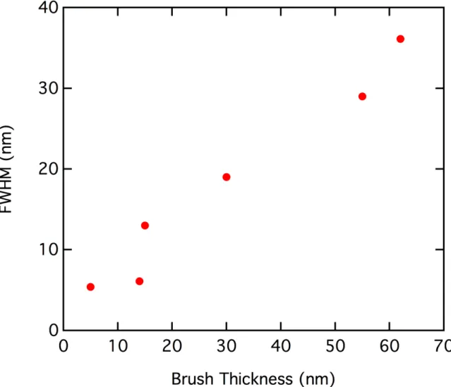
3.10 Comparison of P3MT height distributions for various brush film thicknesses . 58 3.11 Full-width-at-half-maximum of brush height distribution vs. brush thickness 59 3.12 Very short growth time P3MT brush film AFM image . . . 60
3.13 Column masks generated by the column identification algorithm . . . 64
3.14 Column areal density at various area fractions . . . 65
3.15 AFM tip convolution with surface features . . . 67
3.16 Column cross-sectional area measurement . . . 68
3.17 Column cross-sectional area . . . 69
3.18 Column analysis of 32 nm thick brush film . . . 70
3.19 Column analysis of 55 nm thick brush film . . . 71
3.20 Column cross-sectional area vs. area fraction . . . 72
3.21 Height-height correlation function . . . 72
4.1 KTP electrodes printed on P3MT brush film . . . 77
4.2 CPB device schematic . . . 78
4.3 Typical I-V curves from CPB devices . . . 78
4.4 Repeated I-V measurements on single CPB device . . . 79
4.5 I-V curves for 5 nm CPB devices . . . 81
4.6 I-V curves for 6 nm CPB devices . . . 82
4.7 I-V curves for 7 nm CPB devices . . . 83
4.8 I-V curves for 8 nm CPB devices . . . 84
4.10 I-V curves for 22 nm CPB devices . . . 86
4.11 I-V curves for 36 nm CPB devices . . . 87
4.12 I-V curves for 51 nm CPB devices . . . 88
4.13 I-V curves for 53 nm CPB devices . . . 89
4.14 I-V curves for 66 nm CPB devices . . . 90
4.15 I-V curves for 82 nm CPB devices . . . 91
4.16 I-V curves for 91 nm CPB devices . . . 92
4.17 Comparison of I-V Curves for CPB devices . . . 93
4.18 Di↵erential conductance . . . 94
4.19 CPB device resistance . . . 95
4.20 Asymmetry in I-V curves for CPB devices . . . 97
4.21 Log-log I-V behavior for CPB devices (L0 of 5 to 8 nm) . . . 98
4.22 Log-log I-V behavior for CPB devices (L0 of 15 to 36 nm) . . . 99
4.23 Log-log I-V behavior for CPB devices (L0 51 to 91 nm) . . . 100
4.24 KTP pad deformation . . . 102
4.25 AFM image of KTP devices on P3MT brush film . . . 103
4.26 KTP electrode printed on Si substrate . . . 104
4.27 KTP electrode height analysis . . . 105
4.28 Hole injection barriers for CPB devices . . . 111
4.29 Forward bias energy diagram for CPB devices . . . 112
4.30 Reverse bias energy diagram for CPB devices . . . 112
4.31 ILC fits for the forward and reverse bias . . . 115
4.32 ILC fits for thin devices . . . 116
LIST OF ABBREVIATIONS AND SYMBOLS
AFM Atomic Force Microscopy
cAFM Conducting Atomic Force Microscopy CP Conducting Polymer
CPB Conjugated Polymer Brush FWHM Full-Width-at-Half-Maximum
GIWAXS Grazing Incidence Wide Angle X-ray Scattering HOMO Highest Occupied Molecular Orbital
ILC Injection Limited Current ITO Indium Tin Oxide
IV Current-Voltage (i.e. current-voltage measurements) KTP Kinetic Transfer Printing
LUMO Lowest Unoccupied Molecular Orbital µ Charge Carrier Mobility
MMM Metal-Molecule-Metal (i.e. metal-molecule-metal junctions) OSC Organic Semiconductor
P3AT Poly(alkylthiophene) P3MT Poly(3-methylthiophene) P3HT Poly(3-hexylthiophene)
RBS Rutherford Backscattering Spectroscopy SAM Self-assembled Monolayer
STM Scanning Tunneling Microscopy
CHAPTER 1: INTRODUCTION
On October 10, 2000 the Royal Swedish Academy of Sciences awarded the Nobel prize in Chemistry to Alan J. Heeger, Alan G. MacDiarmid and Hideki Shirakawa for their work in the 1970s on “the discovery and development of conductive polymers.”1 Upon their discovery
conducting polymers became an intriguing alternative to traditional inorganic wafer-based technologies which form the bedrock of modern electronics. Conducting polymers belong to a larger class of materials called organic semiconductors (OSCs), which include all carbon based semiconducting molecules and materials. Since the 1970s, researchers have improved the processability, stability, and performance of OSC devices, and worked towards understanding the fundamental mechanisms governing the electronic properties of OSCs. Today, after decades of progress, OSCs see wide commercial use in phone screens and other displays due to their light weight, cheap fabrication, low power usage and potential for high contrast ratios. OSCs have many intriguing properties that distinguish them from inorganic counterparts, which have made them attractive candidates for applications, including transistors, solar cells, and radio-frequency identification devices. Due to both their already realized and potential applications, the global market for organic electronics is expected to grow upwards of $80 billion by 2020.2
While OSCs o↵er many advantages over traditional inorganic materials, and the commer-cial use of OSC devices continues to grow, commercommer-cial applications for OSCs are currently limited.3 OSC devices tend to have lower charge carrier mobilities than their inorganic
coun-terparts. High mobility is essential to the performance of many electronic devices such as transistors and photovoltaics, and increasing the mobility of these devices is a key objective of the field.4 Understanding the processes that control charge transport, and therefore device
Section 1.1: Review of Essential Chemistry
1.1.1: Molecular Orbitals and Conjugation
When atoms come together to form molecules, the electron orbitals of adjacent atoms interact, resulting in new orbitals with di↵erent energies and shapes than the atomic orbitals of the constituents. These new orbitals are called molecular orbitals, and are often interpreted as atoms ‘sharing’ electrons or as bonds which hold the atoms in a molecule together. These orbitals give rise to many of the optical and electronic properties of molecules, and the orbitals which contribute the most to the electronic properties of molecules are the highest occupied molecular orbital (HOMO) and the lowest unoccupied molecular orbital (LUMO). These orbitals correspond to the highest electron energy level that is occupied in the molecule’s ground state and the lowest electron energy level that is unoccupied in the molecule’s ground state respectively, and are analogous to the conduction and valance bands in crystalline solids.
Figure 1.1: Multiple versions of benzene’s structural formula are shown. ⇡ delocalization occurs along the benzene ring and is indicated by alternating single and double bonds. (a) Benzene’s structural formula. (b) The p orbitals of individual carbon atoms in the benzene before they form into delocalized ⇡ orbitals. (c) ⇡ orbitals resulting from p orbital overlap in benzene.
Molecular orbitals are classified as either orbitals or ⇡ orbitals (also called or ⇡
spanning multiple nuclei within the molecule (Figure 1.1). In organic materials ⇡ orbitals tend to be higher energy than orbitals,5 and therefore, in conjugated organic materials the
HOMO and LUMO levels are often ⇡ orbitals.
Figure 1.1 shows the origin of delocalized ⇡ orbitals in benzene. These orbitals are delocalized across the entire benzene ring. In structural formulas the presence of ⇡ orbitals is indicated by the alternating single and double bonds, as can be seen in the benzene ring. Molecules which form delocalized ⇡ orbitals are called conjugated molecules.
1.1.2: Polymers
Polymers are a diverse group of molecules, which display many di↵erent mechanical, chemical, and electronic properties, making them a versatile class of materials. For example, DNA and proteins are polymers. Plastic and rubber are made of polymers. Scotch tape’s stickiness and Teflon’s smoothness both come from the polymers they comprise. The versa-tility of polymers is further augmented by their tunability, e.g. molecular side chains can be added to a polymer backbone to give the polymer new functionalities (Figure 1.3). A poly-mer’s properties can also be adjusted by adding chemical groups to the polymer molecule through a process called functionalization, e.g. adding chemical groups that contain ferro-magnetic metals to allow stronger interaction with ferro-magnetic fields. Due to their incredible versatility, low cost, and processability, polymers have become ubiquitous in our society.
Polymers are molecules formed out of smaller molecular units, called repeat units or monomers (Figure 1.2). Monomers are chemically bound together to form larger polymer molecules. The number of monomers which form a polymer is called the degree of polymer-ization, and can be controlled during polymer synthesis, allowing the molecular weight of the resulting polymer molecule to be tuned. The molecular weight of a polymer can have a large e↵ect on its mechanical, chemical and electronic properties.7 Polymers with few monomers
not used for all polymers, however, as polymers can contain millions of monomers.
Polymers do not generally form rigid, straight structures. Though small polymers tend to behave like rigid rods, above a certain length a polymer’s shape, also known as its con-formation, becomes non-linear (Figure 1.4). For the theoretical ideal polymer, conformation is modeled as a three dimensional random walk.8 The length scale on which the polymer
maintains its tangent orientation is called the persistence length.9 Polymers with longer
per-sistence length have higher rigidity. Conformation can have a large impact on the mechanical, electrical and chemical properties of a polymer and polymer materials, and so controlling polymer conformation is desirable.10
A polymer’s size can be described in multiple ways, the most common being degree of polymerization, molecular weight, contour length, and radius of gyration. The contour length of a polymer describes the distance traced out by the polymer’s backbone and is directly proportional to the number of monomers in the polymer. Degree of polymerization, molecular weight, and contour length are equivalent in that they describe the amount of material in the polymer, but do not contain any information about the polymer’s spatial extent or conformation. The radius of gyration is the root mean square distance of the polymer from its center of mass, and therefore contains information about both the number of monomers in the polymer and its conformation. Since the conformation of large polymers tend to behave like a random walk, the contour length is generally much larger than any one dimension of the volume enclosing the polymer.
1.1.3: Organic Semiconductors
electrodes.12 Building on the semiconducting properties of organic crystals, a new class of
OSCs were discovered in the 1970s: conducting polymers. Small molecules and conducting polymers each have their own advantages as active materials in electronic devices. Conduct-ing polymers o↵er better flexibility and solution processability, while small molecules o↵er high crystallinity.
Conductivity ( ) is a property of materials that relates the current density (J) produced within a material to the electric field (E) is applied to the material. Conductivity is given by
J = E, (1.1)
=neµ, (1.2)
where n is carrier concentration of the material, e is the elementary charge, and µ is the charge carrier mobility. Mobility is discussed further in section 1.2.2. Based on their con-ductivity, materials fall into one of three general categories: insulators, semiconductors and conductors. Insulators are materials with low conductivity, conductors are materials with high conductivity, i.e. metals, and semiconductors for materials which fall in between. Semi-conductors and Semi-conductors are used to build a wide array of circuit elements in electronic devices, and OSCs and conducting polymers fall into either the semiconducting and con-ducting ranges (Table 1.1).
Table 1.1: Conductivities of select materials
Material conductivity (⌦ 1cm 1)
Metals 105
Stretch oriented doped polyacetylene 105
Doped polyacetylene 103 to 105
Undoped polyacetylene 10 5
Insulators 10 8
Teflon 10 20
Conducting polymers are conjugated. In 1949 Kuhn showed that the energy level of ⇡
one dimensional periodically repeating potentials.13 Kuhn’s model for conjugated polymers
draws a parallel to the periodic crystal lattice which gives rise to electronic band structure in solids. Since their discovery in the 1970s, it has been assumed that the delocalized⇡orbitals along the backbone of conjugated polymers should behave similarly to energy bands in crystalline materials, and result in band-like charge transport along the conjugated polymer backbone.14
Conjugation alone is not enough for polymers to conduct, the polymer’s carrier concen-tration needs to be high as well. The intrinsic carrier concenconcen-tration in undoped polymers (ni) is given by
ni =N0exp(
Eg
2kT), (1.3)
where Eg, the energy di↵erence between HOMO and LUMO levels, N0 is the density of
transport states,T is the temperature and k is the Boltzmann constant.5 Larger band gaps
result in lower intrinsic carrier concentration due to the exponentially decreasing probability of electrons thermal excitation from the HOMO to LUMO states as the gap grows larger. Adding a small amount of dopant can greatly increase the carrier concentration of polymer material, similar to doping inorganic semiconductors.15 Dopants in conducting polymers
work by oxidizing or reducing the polymer, adding or removing electrons from its HOMO or LUMO levels.15Carrier concentration can also be increased by injecting charge into the OSC
from an electrode,5 or through photogeneration.16 Atmospheric doping is prevalent in many
OSCs where exposure to atmosphere allows oxygen and water to permeate the material, resulting in oxidation or reduction of molecules within.17
Adding or removing a charge from a molecule can cause a local change in the molecule’s conformation.5 When a charge moves through a polymer, or between polymers, this local
deformation moves with it. The charge carrier and the local deformation around it are often modeled as a quasi-particle called a polaron,5 which behaves much like an electron or hole
The conformation of conducting polymers can have an impact on their conductivity.18 ⇡
conjugation occurs due to the planar nature of monomers in the polymer. If monomers lie in the same plane, their p-orbitals can overlap and delocalized ⇡-orbitals can form. Torsion defects in longer polymers can cause breaks in the coplanarity of monomers and therefore delocalized ⇡ orbitals tend not to extend along the entirety of the conjugated polymer back-bone. Instead, the polymer is segmented into discrete conjugated sections, each with its own delocalized ⇡-orbitals. The size of these segments is called the conjugation length of the polymer. Increasing conjugation length leads to an increase in the conductivity of con-jugated polymers19, likely due to longer conjugation lengths resulting in smaller band gaps
S S
S S S
S S
S S
S S
n
S
n n
Figure 1.3: Polythiophene can be modified with the addition of side chains. (a) Poly(3-hexylthiophene) (P3HT) tetramer, a polytiophene derivative with a hexyl group attached to each monomer. The alternating side chain placement is called regioregularity. The large hexyl side chains result in an increase in solubility.6 (b) P3HT polymer. (c)
Poly(3-methylthiophene) (P3MT), a polythiophene derivative with a methyl group attached to each monomer. Smaller side chains allow denser packing of the polymer, but reduces solubility.
Section 1.2: Organic Electronics
1.2.1: A Brief History and Overview of Organic Electronics
The field of organic electronics encompasses the study of films consisting of conjugated polymers or small organic molecules. In devices, film thickness is generally much greater than the length of the individual molecules within the bulk, so the study of organic electronics is focused on the bulk properties of OSCs and less focused on the properties of individual molecules. The morphology of organic electronic films range from isotropic and amorphous to oriented and crystalline. Due to their wide range of realized and potential uses, organic electronics continue to attract academic and commercial interests.
The first conducting organic material was discovered by Henry Letheby in 1862, and called the “blue substance.”21 The blue substance was later found to be a polymer, polyaniline,
but in 1862 the concept of polymers would not be developed for over half a century. Organic electronic devices were first studied in the 1950s. These devices were crystals made of small organic molecules, and demonstrated the feasibility of organic materials as active elements in electronic devices. Conjugated polymers were discovered in the 1970s, introducing a new class of OSCs that allowed for solution processing and greater flexibility for fabricating organic electronic devices. By the late 1980s, the first practical OLEDs were made,22paving
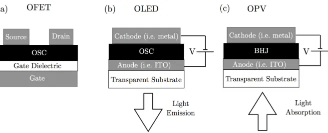
the way for future commercialization of organic electronics (Figure 1.5). The first OFETs were reported in the 1980s as well, utilizing polythiophene as the active semiconducting material in a traditional thin film field e↵ect transistor (TFT) geometry (Figure 1.5).23
While OLEDs matured over the following decades into a commercialized technology that now sees widespread use, OFETs are still an academic research topic and have not yet achieved commercial use. The first organic photovoltaics (OPV) were made in the mid 1990s, initially achieving efficiencies of only ⇠ 3% (Figure 1.5).24 OPVs continue to be an
Figure 1.5: (a) OFETs function identically to traditional TFTs. In OFETs the inorganic semiconductor has been replaced by an organic semiconductor. The low mobility of organic semiconductors makes the switching speed of OFETs much slower than traditional transis-tors. (b) A simple OLED is constructed by placing an an emitting active layer between two electrodes. By applying a bias across the active layer, holes and electrons are injected by the cathode and anode which recombine within the film and emit photons. (c) Photovoltaics operate on very similar principles as OLEDs, except they absorb light rather than emit it. A bias is applied creating an electric field across the active layer. Then when an incoming photon can excite an electron in the active layer from the HOMO to the LUMO creating an electron-hole pair. The electron and hole are drawn to opposite electrodes due to the electric field, and create a current. High mobility helps prevent the electron and hole from recombining within the active layer. The most common design for OPVs uses a bulk hetero-junction as the active layer. In BHJ two conducting polymers are used, one which accepts electrons and on one which donates electrons, called the donor and accepter. The electrons travel to the electrode through the acceptor and the holes travel through the donor.
1.2.2: Charge Transport and Mobility in Organic Semiconductors
Mobility relates the drift velocity of charge carriers within a material to the electric field applied to the material. Holes and electrons can have di↵erent mobilities within the same material. When considering multiple charge carriers, the relationship between mobility, electric field and current density is given by
J =⇢eµeE+⇢hµhE, (1.4)
and holes, and E is the applied field. Since the intrinsic carrier concentration for OSCs are very low, in many devices extrinsic charge carriers are injected from electrodes to increase carrier concentration.5 In these devices carrier concentrations are largely controlled by the
electrode-OSC interface.25In order to simplify the interpretation of electronic measurements,
electrodes are often selected such that unipolar transport occurs, where one charge carrier has a significantly higher concentration than the other. Interfaces are described in more detail in section 1.2.3. By allowing one predominant charge carrier, the relationship between current density, electric field, and mobility can be expressed using equations 1.1 and 1.2. Though the SI units for mobility are m2/V-s, mobility is conventionally measured in units
of cm2/V-s.25
Charge carrier mobility is the natural benchmark for describing and comparing organic electronic materials.3,26–28 In many active devices such as OPVs and OFETs, high mobility
is essential for device performance. A driving force of the field is to find materials and build devices with mobilities approaching their inorganic counterparts. A comparison of mobility for select organic and inorganic semiconductors is shown in Table 1.2.
Table 1.2: Mobilities of select materials
Material Mobilityµ(cm2
V s)
Single crystal Si 450 (hole) to 1400 (electron)
Highest mobility organic single crystal devices29 40
Amorphous Si 1
Highest mobility CP devices29 ⇠10
Spuncast Poly(3-methylthiophene)17 0.004
Organic electronic devices can often have performance reproducibility issues due to device-to-device morphological fluctuations30,31 and sensitivity to fabrication and post
treat-ment procedures.31 Di↵erent measurement techniques used on the same device can also
produce drastically di↵erent mobilities, and the same data can result in very di↵erent ex-tracted mobilities depending on who is analyzing the data.32 Despite this, mobility remains
transport in organic electronic devices is essential for building high performance devices. In organic electronic films, transport occurs not only along the backbone of individual polymer chains (intramolecular) but also between polymers (intermolecular) (Figure 1.6). Transport is a combination of band like drift through conjugated segments of polymer back-bone interspersed with hopping between conjugated segments both along a single polymer, and between adjacent polymers.33 Hopping between polymers typically occurs through ⇡
-stacks (Figure 1.6).25 ⇡ stacking is the result of attractive interactions between⇡ orbitals on
aromatic rings which cause them to align (Figure 1.6). ⇡ stacking can occur in films made of polymers which contain conjugated aromatic rings, such as polythiophene. Hopping typ-ically refers to a thermally activated process, characterized by an activation energy, where charges are excited over a potential barrier separating molecular orbitals.
Both experimental and theoretical reports show that increased intramolecular trans-port results in increased bulk mobility in organic electronic devices.34–36 The mobility of
intramolecular charge transport through conjugated segments on ordered polymer chains is expected to be on the order of a few hundred cmV-s2), but these mobilities have not been observed due to the inherent disorder in conducting polymer films.37 In particular, device
ge-ometry often necessitates intermolecular charge transport and charge transport across grain boundaries, which are both significantly slower than intramolecular transport.37
Addition-ally, disorders in films can limit the conjugation length of conducting polymers, creating additional transport barriers.37 Designing devices to take advantage of the intramolecular
transport in order to achieve higher mobility is a common practice.
Directly probing mobility requires transient measurement techniques that often require specialized instrumentation such as extremely high gain-bandwidth product amplifiers to detect small and fast signals, or restrictive device and material properties, such as min-imum device thicknesses, or materials with conductivities that meet certain thresholds.32
measurements a bias is applied across a device and the current response is observed. The measured current response is a result of both inter- and intramolecular transport, and it is difficult or impossible to deconvolute the contribution of each e↵ect.
Electrode Electrode Vbias (a) Electrode Electrode Vbias Electrode Electrode Vbias (c)
Decreased E field at the injection interface.
E field at the injection interface becomes 0. Constant E field across the device.
Active Layer Active Layer Active Layer
Injection Limited Regime
(b)
Intermediate Regime
Space Charge Limited Regime
Common techniques used to study charge transport in organic electronics include space-charge limited current (SCLC) methods, field-e↵ect transistor measurements, and current extraction through linearly increasing voltage (CELIV).38 SCLC is one of the most widely
used models for extracting mobility from IV curves. SCLC is an attractive model because it requires a simple experimental setup ans is easy to implement.32Like most models employed
to probe mobility in organic electronics, the technique was originally developed for inorganic systems. The model assumes that charge carriers are injected into the device much faster than they can move through the device and therefore a net charge density (space-charge) builds up within the material. This space-charge generates an electric field which opposes the field at the injecting contact. As charge builds within the material, the opposing electric field builds, until the net field at the injecting contact is 0 (Figure 1.7). The equation for SCLC is given by
J = 9 8µ✏r✏0
V2
L3, (1.5)
where J is the current density,✏ris the dielectric constant of the material,✏0is the vacuum
permittivity, V is the applied bias, and L is the distance between electrodes. Mobility is extracted when a quadratic relationship betweenJ andV is observed, which often occurs at high biases. However, simply observing a quadratic relationship is not enough to determine if SCLC is occurring and if the model is correct.
The erroneous application of the SCLC model to systems which do not satisfy SCLC’s underlying assumptions can result in extracting incorrect mobilities (Figure 1.8).39 If the
resulting injection barrier of the injecting electrode is too large, or the applied bias is too small, the space-charge limited transport regime will not be reached and mobility will be underestimated.39 The characteristic J ⇠ V2 relationship is often observed even outside of
the SCLC regime,39 so goodness of fit is not sufficient to justify the SCLC model. Tuning
Figure 1.8: Linearized data and SCLC fit for mobility extraction. Three electrodes made of di↵erent metals were deposited on a single OSC film. Extracted mobility spans two orders of magnitude and depends on the work function of the metal electrode (i.e. the size of the injection barrier), indicating that the SCLC model is inadequate to describe transport for these devices. Figure 2 in Ref [39], reproduced with permission.
measurements.27,39
1.2.3: Metal - Organic Semiconductor Interfaces
For many OSC devices, electrodes are used to extract and inject charge carriers into the active layer. The interfaces between the electrodes and the OSC have a large e↵ect on the electronic characteristics of a device.27,39 For conducting polymers, understanding the
electrode-polymer interface is essential in order to interpreting electronic measurements of the polymer.
In many organic electronic devices charge carriers are injected from metal electrodes into molecular orbitals within the active layer.5 Generally, electrode work function falls between
charge carrier must overcome (Figure 1.9). This requires thermal excitation, or tunneling through the barrier. The larger the injection barrier and the lower the temperature, the harder it is for charge carriers to be injected.40 The size of the injection barrier for electrons
(holes) is determined by the energy di↵erence between the electrode work function and the LUMO (HOMO) energy level at the polymer-electrode interface.40 The majority charge
carrier is determined by the carriers with the lowest injection barrier.
Figure 1.9: Charge injection from electrodes into polymer must occur at the electrode-polymer interface. (a) The energy level alignment of a metal electrode and an organic semiconductor at the interface. (b) The resulting injection barriers for holes and electrons. The size of the injection barrier is determined by the distance between the metal’s fermi level and the HOMO (holes) or LUMO (electrons) levels.
When OSCs and electrode come into contact, deformation of the HOMO and LUMO levels can occur, much like band bending in inorganic semiconductors. However, a naive, but attractive model for the resulting barrier at the OSC-electrode interface is the vacuum level alignment, or Schottky-Mott rule.41 In this model, the fermi level of the OSC moves
LUMO levels of the OSC.41 The resulting injection barrier is just the di↵erence between
the metal work function and the HOMO level for holes, or the metal work function and the LUMO level for electrons (Figure 1.9). In this model, the injection barrier can be made arbitrarily small for the charge carrier of choice by picking electrodes whose work function matches the HOMO or LUMO level of the OSC.41 In practice, low injection barriers are
generally desired,38 leading to ‘ohmic contacts’, contacts with an injection barrier small
enough that the current through the device is not limited by the injection barrier, but by other processes such as charge carrier scattering or space-charge buildup. Ohmic contact are required for SCLC.39
In general energy level alignment at electrode-OSC interfaces is more complicated than the vacuum level alignment model. When the fermi level of the electrode is far from the HOMO or LUMO levels of the OSC, vacuum level alignment is an accurate model, and the interfacial behavior is well described by the Schottky-Mott rule.42 However, when the
electrode fermi level is close to the HOMO or LUMO level of the OSC, charge transfer can occur between the electrode and the OSC causing a dipole to form and vacuum level alignment to no longer be an accurate model. For a given material the onset of charge transfer appears to occur at a constant energy relative to the HOMO and LUMO levels, often referred to as the pinning energies or charge transfer onset energies ( + and ).42
There are many competing theories for why this charge transfer occurs, and why pinning occurs at specific energies for a given material. Some explanations include the formation of polaron states forming at energies close to the HOMO or LUMO level,43or metal induced gap
states (MIGS) due to the electronic states of the metal electrode interacting with the OSC and inducing states around the HOMO and LUMO levels near the interface,44 among other
models.42 The cause of the phenomena is debated,42 but there is a consensus that charge
HUMO and LUMO level where there are no electronic states in the OSC, and therefore no charge transfer or band bending occurs (Figure 1.10). The phenomenon is well documented both experimentally (Figure 1.11) and theoretically,41,42,45 and results in a minimum energy
Figure 1.11: Transition between vacuum level alignment and fermi level pinning at metal-OSC interfaces. In this figure EICT+ and EICT correspond to + and in Figure 1.10.
The work function of many OSCs was measured on di↵erent substrates by ultraviolet photo-electron spectroscopy (UPS). The work function of the OSCs is equal to the work function of the work function of their substrates in the middle part of the graph, consistent with vacuum level alignment as shown in (b) of Figure 1.10. When the substrate’s work function becomes close to the HOMO or LUMO levels of the OSC and hits the pinning energies ( +
or ) the work function of the OSC becomes pinned, which results in a constant OSC work function when the substrate work function is above (below) + ( ). When the OSC work
Section 1.3: Molecular Electronics
1.3.1: A Brief History and Overview of Molecular Electronics
Molecular electronics is the study of molecules as individual electronic components, as opposed to the properties of OSCs.46 Molecular electronics includes the study of both single
molecules and ensembles of parallel molecules. Molecular wires are often presented as the ultimate nanoscale building block,47and the smallest conceivable stable structures which can be integrated into an electronic circuit.48 Potential uses for molecular wires include memory
storage and transistors,48but commercial devices incorporating molecular wires are currently
a distant goal.
Self-assembled monolayers (SAMs) are one of the most common molecular wire ensembles studied. SAMs consist of a single layer of aligned molecules on a substrate. Molecules in SAMs often have a ‘head’ group on one end that interacts strongly with the substrate, and a ‘tail’ group which orients away from the substrate at some tilt angle relative to the normal. SAMs can be covalently bound to the substrate, or interact with the substrate through weaker Van der Waals forces. Functional groups can be attached to the end of the tail on SAMs to tune the properties of the monolayer, such as making the SAM interact more strongly with a top electrode.
The electronic properties of molecular wires were first probed in the early 1980s after the development of the STM.49 Measurements on single molecules with an STM tip are transient
in nature. In these measurements a conducting tip is brought into contact with one end of a molecular wire that has been grown from or attached to a conducting substrate.49 A
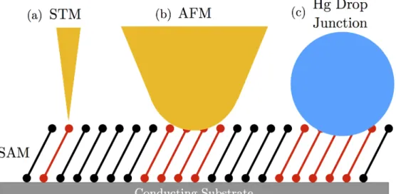
temporary metal-molecule-metal (MMM) junction is formed with the conducting tip acting as one electrode and the substrate acting as the other electrode. After the measurement is over the tip moves on to a new molecule to form a new junction. The transient nature of the STM-based junction is a common in MMM junctions.49
metal-molecule interfaces. Each part of the MMM can be tuned individually to a↵ect the per-formance and properties of the junction. Di↵erent metals can be used for the electrodes. Di↵erent linker groups can be used in the interfaces to attach the molecule to the electrodes, or the linker groups can be foregone completely. Di↵erent molecules can be put inside the junction. MMM junctions can contain a single or multiple molecules,47 but every molecule
must touch both electrodes. The electronic properties of single molecule junctions can be difficult to measure for larger molecules. The resistance of individual molecules is quite large, and so the current response for large single molecules can be immeasurably small at low biases. Multiple molecular wires act as parallel resistors, so adding more molecules to a junction lowers its resistance.47 Junctions containing multiple molecular wires are usually
necessary for measurements on longer molecules.
Figure 1.12: Schematics for some common MMM junctions are shown. (a) An STM MMM junction. STMs have the resolution to address single molecules with their conducting tips, allowing the electronic properties of single molecular wires to be probed. (b) AFM tip contacting a SAM. AFM tips are much larger than STM tips and address hundreds of molecules simultaneously. (c) Hg drop junction. In these junctions a liquid Hg drop is put on the end of a wire and brought in contact with a SAM. These junctions address 1010 to
1011 molecules.
MMM devices are transient and permanent molecular electronics devices are not widely used. Creating permanent contacts is difficult for single molecule junctions since their locations must be precise on an atomic scale.47For devices which include multiple molecular wires, the
contact locations do not need to be as precise as for a single molecule, but the monolayers used in molecular electronics tend to be very thin (<20 nm) and depositing contacts without shorting through the monolayer is difficult.47 Some techniques, such as transfer printing, do
allow permanent contacts to be made on top of SAMs, but these permanent contacts still can only be addressed by AFM or similar techniques.48
1.3.2: Charge Transport in Molecular Wires: From Tunneling to Hopping
Unlike organic thin films, the concept of mobility is often not applicable to molecular electronics. Mobility is a measure of a charge carrier’s drift velocity, and molecular wires are usually not long enough for the concept of a drift velocity to make sense.40For short molecular
wires the charge carrier never directly enters the material, instead tunneling directly from electrode to electrode. Tunneling current can be modeled using the Simmons model50
I = qA 4⇡2¯hd2
0 "
( qV 2 )exp
h 2(2m)1 2 ¯ h ↵(
qV 2 )
1 2d0
i
( +qV 2 )exp
h 2(2m)1 2 ¯
h ↵( + qV
2 ) 1 2d0
i#
,
(1.6) where I is the current, q the electron charge, A is the area of the junction, ¯h is the reduced Planck constant,d0 is the tunneling distance, is the tunneling barrier height,V is
the applied bias, andm is the charge carrier’s e↵ective mass. While the full current voltage dependence of devices is often probed for molecular wires, one essential benchmark is the relationship between a molecular wire’s length and its zero-bias resistance.51 The zero-bias
R =R0e d0and (1.7)
= 2(2m )12/¯h, (1.8)
where R is the resistance, R0 is a contact resistance,d0 is the molecular length,m is the
e↵ective mass of the charge carrier, is the height of the tunneling barrier, and is the tunneling decay coefficient which describes the efficiency charges tunnel through a material.51
is measured by plotting log resistance vs length and measuring the slope of the line.52Since
the tunneling probability depends exponentially on length, the semilog plot should be linear. The parameter is widely used across the field as a benchmark for characterizing molecular wires.51
Tunneling usually only occurs in molecular wires less than 5 nm in length,51 and in this
length regime the resistance of the molecule depends exponentially on the molecule’s length. As the molecule gets longer a transition is observed in the length dependence of molecule’s resistance (Figure 1.13).51The relationship between a molecular wire’s resistance and length
transitions from exponential to linear as the molecule becomes longer, indicating a transition in charge transport mechanism.51 For longer molecules, charge is injected into the molecular
wire (or wires) instead of tunneling through them, and band-like or hopping transport occurs through molecular orbitals along the molecule or molecules.51
Molecular junctions are expected to exhibit some finite contact resistance, which is de-termined by extrapolating the resistance of the device at 0 length. However, for molecular electronics, extrapolating the resistance at 0 length using the linear regime of the resistance vs. length plot will result in a negative resistance.51 This phenomenon occurs in both single
Figure 1.13: A transition between exponential and linear relationship between molecular length and resistance is shown. The transition indicates a change from direct tunneling between electrodes to hopping transport within the molecule. Figure 3 in Ref [53], reproduced with permission.
2-5 nm as well).40 Because of this, the distance that the charge carriers travel through the
active layer is less than the total molecule length and the total thickness of the device. While covalent linkage of molecular wires to one or both electrodes in molecular elec-tronics devices has allowed the study of transport along single molecules, the strategy is not scalable to longer molecule lengths due to synthetic and technical limitations.54 Molecular
Section 1.4: Polymer Brushes
Polymer brushes are microstructures made of densely packed polymer chains which are immobilized at one end, i.e. attached to a substrate surface or fluid interface.55 This
immo-bilization of one end of the polymer coupled with dense packing forces polymer-polymer in-teractions which causes the polymers to ‘stretch out’ into a ‘brush’ conformation.55 Halperin
et al. suggest that polymer brushes grow predominantly perpendicular to the surface on which they are immobilized. The thickness of a brush film, L, is given by
L b =N(
b d)
2
3, (1.9)
whereN is the number of monomers in the polymer,bis the length of a monomer, anddis the spacing between adjacent polymer chains.55 For a given molecular weight, more densely
packed brushes (i.e. brushes with low d) should result in longer, less isotropic, polymer brush films. Thus, the grafting density of polymer brushes has a very large impact on the conformation on polymers within the brush.55
Like SAMs, polymer brushes are grafted to a substrate; however, they can be grown much longer than SAMs.54 Electronic devices comprising polymer brushes can be made by
CHAPTER 2: EXPERIMENTAL METHODS Section 2.1: P3MT Brush Synthesis and Device Fabrication
P3MT brush growth occurs in solution. There are two main mechanisms by which solu-tion polymerizasolu-tion can occur: chain growth and step growth.56Chain growth polymerization
describes the sequential addition of single monomers to a propagating polymer chain, while step growth polymerization corresponds to monomers forming dimers, then larger oligomers, then oligomers coming together to form larger polymers. For P3MT brushes, greater control over brush length and packing density is desired, so chain growth polymerization techniques are used.57 The reactive polymer chain is attached to a surface, and monomers are inserted
onto a propagating chain one at a time.
The P3MT brush is grown through a process called Surface Initiated Kumada Catalyst-Transfer Polycondensation (SI-KCTP). A distinguishing characteristic that separates KCTP from other chain growth polymerization techniques is the ability for a catalyst to stay as-sociated with one chain during the course of polymerization. After the addition of each monomer, the catalyst undergoes oxidative addition into the terminal carbon-halogen bond of the chain (Figure 2.1).58 SI-KCTP has been demonstrated to produce P3MT films with
some degree of vertical orientation from a conductive substrate.57 The SI-KCTP growth
mechanism follows living chain growth kinetics, meaning it is sensitive to parameters such as monomer concentration and temperature, and that the degree of polymerization of poly-mers within the brush is expected to increase linearly with reaction extent, resulting in low polydispersity (i.e. polymers have a fairly uniform length.)59
hydroxy-Figure 2.1: (a) A clean ITO substrate. (b) The substrate is functionalized with a seed monolayer. (c) The monolayer is initiated with Pd catalyst. (d) An initial monomer is grafted to the seed monolayer and polymerization (e) begins.
lation, such as indium tin oxide (ITO) or SiO2, forming a monolayer on the substrate surface
Figure 2.2: The essential molecules used in brush growth. (a) Brominated phosphonic acid, (b) catalyst, and (c) monomer.
Each phosphonic acid molecule acts as a potential anchor site from which P3MT chains can grow, and is referred to as a seed monolayer. After the substrate surface is functionalized by the phosphonic acid monolayer, a catalyst initiator (Figure 2.2b) is added. The catalyst allows KCTP to occur. While multiple catalysts have been previously reported for SI-KCTP, Pd was chosen over Ni to reduce disproportionation61 (the tendency of intermediate
products in a chemical reaction to form into undesired compounds) and because polymer brushes grown using a Ni catalyst require prohibitively insulating monolayers to achieve vertical anisotropy.54,64 Molecules within the monolayer must be initiated by the Pd catalyst
in order to grow polymer chains, and not all molecules in the seed monolayer are initiated.57
Figure 2.3: AFM images of two substrates used for brush growth. Both images are 5µm x 5µm. (a) ITO has characteristic grains and an RMS roughness of 0.6 nm. (b) SiO2 has an
RMS roughness of 0.2 nm.
3-methylthiophene monomers were selected for brush synthesis, to produce a Poly(3-methylthiophene) (P3MT) brush. P3MT is a derivative of polythiophene, a model conduct-ing polymer, and exhibits high graftconduct-ing density in Pd-catalyzed SI-KCTP.57Polythiophene is
a widely studied conducting polymer, and the polythiophene derivative P3HT has received a large amount of interest due to the increased solubility conferred by its long hexyl side chains which allow it to be solution processed.65 Solution processablity refers to the capacity for
soluble polymers to be deposited on substrates from solution by inkjet printing, spin-coating, or other solution-based methods.66These techniques allow for scalable device fabrication due
to the ability to uniformly coat substrates with very large areas.62Conjugated polymers tend
to have low solubility due to the strong interaction between the ⇡ orbitals between chains,62
and often can grow no longer than a few monomers before precipitating. Adding long alkyl side chains to conjugated polymers can increase their solubility.67 While the long hexyl side
chains make P3HT attractive for solution processing techniques, the long side chains prevent efficient brush growth.68
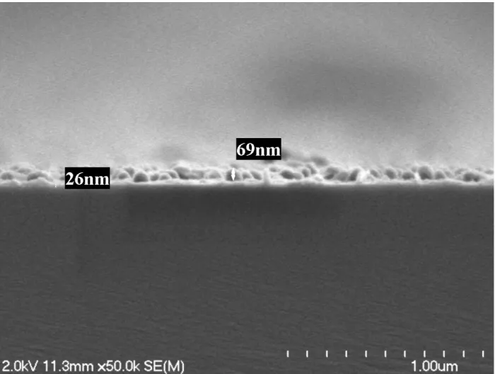
remaining active chains, and the brush is thoroughly washed to remove excess catalyst, solvent and solutes such as left over monomer, Mg, and Cl. In this work, brushes were grown to thicknesses up to 100 nm. An “edge-view” SEM image of a grown brush is shown in Figure 2.4. The brush has an interesting morphology, much di↵erent than a solution processed films which tend to have a smooth surface and uniform film thickness. The brush is covered with “tall” features, termed as “columns”.
Figure 2.4: An SEM image of a P3MT brush grown on an Si/SiO2 substrate
2.1.1: Experimental Procedure
otherwise noted. Dry THF was purified by distillation, and dry toluene (Fisher Chemicals) was used without further purification. Indium tin oxide (ITO) slides (1 inch x 1 inch, 145 nm sputtered ITO, sheet resistance 20⌦/sq) and Si wafers (300 nm wet thermal oxide) were purchased from Thin Film Devices, Inc. and University Wafer, respectively. Au targets for sputtering were purchased from Kurt J. Lesker. bromo-3-methyl-5-iodothiophene, 2-ferrocenyl-5-bromothiophene, (4-bromobenzyl)phosphonic acid, and magnessiated 2-bromo-3-methyl-5-iodothiophene were synthesized using established procedures.60,61
Preparation of ITO Substrates. ITO slides were sonicated in 18 M⌦deionized water, acetone, and isopropanol for 15 minutes each, then placed in RCA cleaning solution (5:1:1 H2O:H2O2:N H4OH) for an hour. After rinsing with water, isopropanol and drying under a
stream ofN2, the slides were cleaned with UV/ozone (Jelight Company Inc., model 42A) for
15 minutes. They were then immersed in an 8-slot staining dish with 30 mL absolute ethanol containing (4-bromobenzyl)phosphonic acid (75 mg, 0.3 mmol) overnight. They were quickly dried under a stream ofN2 and heated in a glovebox at 150 C overnight. Lastly, the slides
were cleaned with water and ethanol and dried under N2 to yield monolayer-functionalized
ITO.
Surface Initiated Kumada Catalyst Transfer Polycondensation (SI-KCTP) Methodology. SI-KCTP was adapted from a previous report.61 Pd-catalyzed SI-KCTP
was chosen over Ni to reduce disproportionation61and because polymer brushes grown using
a Ni catalyst require prohibitively insulating monolayers to achieve vertical anisotropy.64 Monolayer-functionalized ITO slides were initially placed in a staining dish containing a 10 mM solution of P d(PtBu
3)2 in dry toluene at 70 C for 3 hours in a glovebox without
Kinetic Transfer Printing (KTP) Process. This procedure was used to produce electrode-conjugated polymer brush-electrode devices for electrical measurements. A crosslinked poly(dimethylsiloxane) (PDMS) stamp (mixed 3.5:1 by weight with cross-linker, approx. 1 cm x 1 cm, Sylgard 184 Elastomer Kit, Dow Corning) was brought into conformal contact with the donor substrate. The stamp was quickly removed from the surface of the donor using pressure applied with a glass slide (rate of removal > 10 cm/s), transferring the Au features onto the stamp. The “inked” stamp was brought into conformal contact with the receiving substrate (e.g. the brush film) with approximately 1 N of applied force, and re-moved very slowly (⇠0.5 mm/s), transferring the Au features onto the receiving substrate. The PDMS stamp was cleaned to remove particulates between each transfer using scotch tape.
Section 2.2: Bulk Structure Measurements
2.2.1: Cyclic Voltammetry
CV is an electrochemical measurement where a potential is applied across a device, linearly increasing from an initial potential to a maximum potential then decreasing to the original potential. The response current is measured as a function of potential. CV is generally conducted in solution, with the material being probed deposited on a conducting substrate which acts as one electrode, and the solution acting as the other electrode.69 Peaks
in the current vs potential plot form at potentials where oxidation and reduction occur, giving rise to the characteristic “duck” shape of cyclic voltammograms (Figure 2.5).69 The
area under these peaks corresponds to the amount of material undergoing the reaction.69
Films for CV measurements of Pd initiator density were prepared similarly to those used to grow conjugated polymer brush films. After oxidative insertion of Pd(PtBu
3)2 into
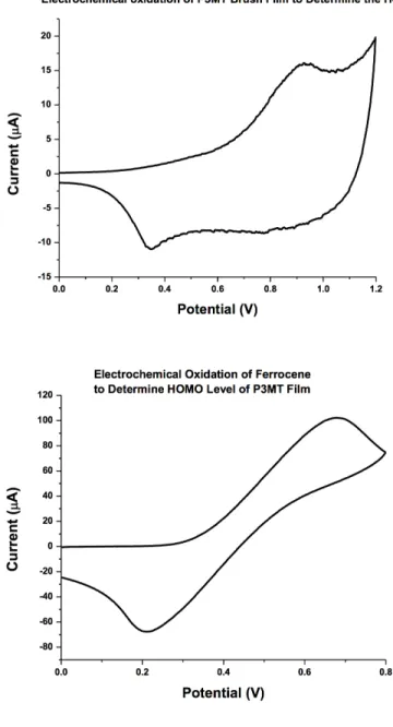
monomer for SI-KCTP) overnight without stirring, then sonicated in chloroform, water, and isopropanol to yield ferrocene-capped monolayers with a density equal to the Pd ini-tiator density. CV was performed in a custom 3-electrode electrochemical cell with the ITO substrate of the ferrocene-modified films acting as the working electrode, a platinum wire counter electrode, and Ag/AgCl reference electrode.63 Tetra(n-butylammonium
hex-afluorophosphate) was the electrolyte (0.1 M) in thoroughly deoxygenated dichloromethane. Scans of ferrocene-capped monolayers on ITO were performed using a BASi Epsilon poten-tiostat, scanning from 0 to +1.2 V at 100 mV/s with several scans to allow for equilibration. The integrated oxidation peak was then used to calculate the surface density of the capped monolayer.
Figure 2.5: (a) structure and (b) cyclic voltammogram of ferrocene-capped bromoben-zyl(phosphonic acid) monolayer. The oxidation peak area (80µA) corresponds to 1.3⇤1014
initiators/cm2. Figure S2 in [54], reproduced with permission.
cyclic voltammetry. The ITO substrate the films are grown from is used as the working electrode with a platinum counter electrode and silver pseudoreference electrode used as supporting electrodes in dichloromethane tetra(n-butylammonium hexaflouorophospate) as the electrolyte. Cyclic voltammograms are taken by positively biasing the working electrode to reversibly oxidize the P3MT film. The onset of the oxidation wave corresponds to removing electrons from the film and is associated with the HOMO level of the polymer brush thin film. The HOMO level is calculated by using a ferrocene standard, and the HOMO level for the P3MT Brush is calculated to be -5.02 eV, corresponding closely to the HOMO level of spuncast films of P3HT at -5.1 eV. There were no observable peaks when applying a negative bias to the film, so the LUMO level cannot be measured in this way. This is not uncommon for polymer films, where often only the electrochemical HOMO level is reported.
2.2.2: Rutherford Backscattering Spectroscopy
Rutherford Backscattering Spectrometry (RBS) is a technique used to analyze the com-position of thin inorganic films, and can determine the thickness, depth and elemental compo-sition of individual layers within multi-layered films. RBS has also been used to characterize the composition of organic films, but it is not a widely used technique within the organic and molecular electronics communities.70 The high energy nature of the measurement, which
re-quires bombarding a film with a beam of nuclei, can damage the more fragile organic films.71
If a significant amount of organic material is ejected from the film by the nuclei, the thickness of the film may change during measurement, making it difficult to interpret data.
Measurement of the density of spin cast P3HT films by RBS has been previously re-ported.72 The average density of P3HT films was found to be 1.33 g/cm3. To calculate this
Figure 2.6: Cyclic voltammetry is performed to determine HOMO level of P3MT brushes. Reprinted with Permission from Travis LaJoie’s Ph. D. Dissertation.57
volume is multiplied by the mass of the P3HT monomer to calculate the density of the P3HT film.
Figure 2.7: Repeated measurements on the same P3MT brush show no loss of sulfur signal, indicating no significant damage was done to the brush during measurement. The integrated S peak contained ⇠400 counts in the first run, and ⇠425 counts in the second run.
Br per polymer chain and one S for each monomer in the film. The degree of polymerization of the P3HT film is therefore given by the ratio of the areal densities of S and Br.70
Experimental Procedures. RBS measurements were performed at the Triangle Uni-versities Nuclear Laboratory (TUNL) where a beam of 2MeV 4He2+ particles was provided
was not significant (Figure 2.7). The program SIMNRA73 was used to calculate the areal
density of sulfur and bromine atoms within the brush by fitting the simulated spectra to the measurement.
2.2.3: Grazing Incidence Wide Angle X-ray Scattering (GIWAXS)
Grazing Incidence Wide Angle X-ray Scattering (GIWAXS) is an X-ray di↵raction tech-nique used for probing molecular length-scale structure in thin films. The wide scattering angle collected during measurement correspond to large values of momentum transfer, which correspond to small distances. GIWAXS has been used extensively to determine the crystal structure of polymer films.36,74–76 For conjugated polymers that have aromatic rings, and
therefore exhibit ⇡ stacking behavior, the crystal structure is well known.77 Polymers align
in two dimensional planes, or lamellae, which stack on top of each other due to the attractive interaction of ⇡ orbital between neighboring polymers (Figure 2.8).77
Experimental Procedures. GIWAXS experiments were conducted at beamline 7.3.3 at the Advanced Light Source at Lawrence Berkeley National Laboratory. The collimated 10 keV beam was approximately 300 µm high and 800µm wide. Its angle of incidence from the surface plane was 0.14 , penetrating the grafted film and experiencing total internal reflection at the glass substrate. A 2 M pixel Pilatus detector was used at a distance of 262 mm, calibrated by the use of a silver behenate standard. Data were reduced using the Nika software package.78 The q values were converted to d values using d= 2⇡/q.
Section 2.3: Surface Morphology
Figure 2.8: (a) The crystal structure of P3MT. The lattice vectors are defined along the chain axis (001), the ⇡-⇡ axis (010), and the lamellar axis (100). (b) A top down view of the P3MT lattice along the chain axis in real space. The reciprocal space vectors detected by GIWAX are the (020) and (110) vectors, which are 3.5 ˚A and 5.2 ˚A respectively (see Morphology section).
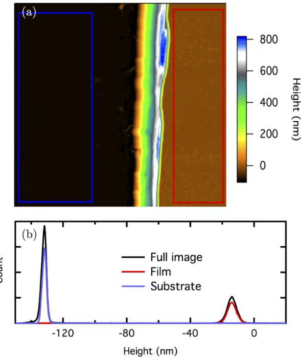
scratched using a 20 gauge steel needle and the scratched step was imaged using the AFM. The film thickness is defined as the peak-to-peak height di↵erence between the respective height histograms of the ITO surface and brush film surface. The I-V measurement circuit is shown in Figure 2.9.
Figure 2.9: The circuit diagram for cAFM used in CPB device measurements. (a) The conducting tip, held at ground. (b) The CPB film. (c) The conducting substrate. (d) The low gain current channel. (e) The high gain current channel. Having a low and high gain current channel allows a larger range of currents to be detected with high precision. The gain of (d) and (e) could be adjusted by changing resistors R1, R2 and R3.
2.3.2: Height-Height Correlation Function
The height-height correlation function, g(r), was used to probe the characteristic length scales of the surface features in the AFM images of the P3MT brush films.79,80 The g(r)
between two points on a surface separated by radius r is given by
g(r) =<[h(x, y) h(x0, y0)]2 >, (2.1)
r=q(x x0)2+ (y y0
whereh(x, y) is the height at position (x, y). Theg(r) functions were first calculated from the AFM topography images and then fit using the phenomenological form
g(r) = 2 2(1 e (r/⇠)2↵), (2.3)
where ⇠ is the correlation length, ↵ is the Hurst parameter (corresponding to a measure of short-range roughness), and is the root-mean-square (RMS) roughness of the surface.
Section 2.4: Electronic Measurements
2.4.1: Conductive AFM (cAFM) Measurements.
CHAPTER 3: P3MT BRUSH STRUCTURE AND MORPHOLOGY Understanding the morphology of the P3MT brush films is necessary for interpreting the behavior of electronic devices utilizing the films. Here, the structure and morphology of P3MT brush film characteristic surface features and their size and distributions are described and analyzed.
Section 3.1: Bulk Measurements
3.1.1: Brush Density
During brush growth, only the molecules in the seed monolayer which have been initiated by the Pd catalyst are able to grow polymer chains, though a polymer will not necessarily graft to all initiated molecules in the monolayer.63 An upper limit on the grafting density
of polymer chains in the brush film can be determined by measuring the catalyst initia-tor density. After initiating the seed monolayer, but before polymer growth, the initiated molecules in the monolayer are functionalized with a a ferrocene functional group, which can be detected through cyclic voltammetry (CV).
Using CV measurements, a catalyst initiator density of 1.3±0.2 nm 2 was determined,57 similar to previously reported results.61,63 However, during polymer growth a color change
limit on the density of polymer chains within the brush.
The density of the polymer near the surface of the substrate can be extracted from the Pd initiator density if it is assumed that all initiated molecules grow polymer chains. Under this assumption, the initiator density corresponds to one chain per 1.3 ± 0.2 nm2. The
spacing between monomers along a P3MT chain is 4 ˚A.81 Therefore, near the surface of the
substrate, the monomer density (monomers per unit volume) is estimated to be 3.3 ± 0.5 nm 3.
The density of the P3MT brush films was probed using RBS. The summed spectra of repeated RBS runs for a P3MT brush film is shown in figure 3.1. The thickness and composition of the SiO2 substrate as well as the areal density of the S in the brush were
simulated using SIMNRA. An areal density of 100 ± 4 atoms nm 2 was found for S, and a
thickness of 260 nm and a composition of 1:2 Si:O was found for the SiO2 layer, in agreement
with the substrates specifications. Due to a low number of counts the Br peak was not fit, instead the peak for the expected Br areal density of 4 atoms nm 2 (from CV) is shown. Trace amounts of Cl appear in the RBS spectra, which is a byproduct of polymerization that was not fully removed during post-polymerization cleaning of the film. Trace amounts of Pd are also present.
The average brush film thickness for the sample, 36 ±2 nm, was measured using scratch AFM profilometry (determining brush thickness by AFM is discussed in detail below). A P3MT brush density of 0.36 g/cm3 was determined. For the RBS result shown in Figure
3.1, the monomer density (number of monomers per unit volume) was found to be 2.8± 0.4 nm 3, compared to a monomer density of 5 nm 3 previously reported for the P3HT films.72
Figure 3.1: (a) The summed spectra of two RBS runs on the same 36 nm sample is shown, along with the SIMNRA fit for elemental composition on the brush and substrate. A thick-ness of 260 nm and a composition of 1:2 Si:O was found for the SiO2 layer, in agreement with
the substrates specifications. (b) The RBS spectrum zoomed into the channels correspond-ing to elements found in the brush. An areal density of 100 ± 4 atoms nm 2 was extracted
for S. The Br peak was not fit due to low statistics, instead the expected areal density of 4 atoms nm 2 is shown. Trace amounts of Cl and Pd are present. Cl is a byproduct of P3MT
polymerization, and Pd is present in the catalyst used for polymerization.
and 1.8 ˚A 1, while the measurement of thinner films yielded negligible di↵raction intensities
(Figure 3.2). The two arcs can be assigned to the (020) and (110) reflections respectively, based on a crystal structure with staggered sheets (⇡-⇡ and lamellar lattice spacing of 3.5 and 7.7 ˚A, respectively).77 The ⇡-⇡ and lamellar lattice spacings extracted from GIWAXS
agree with previously reported values.77 The two lattice vectors are orthogonal to the chain
axis and exhibit a nearly isotropic distribution with a small amount of horizontal texture (Figure 3.3).
The lattice spacing of thiophene along the chain axis is 4 ˚A.81 Together with the⇡-⇡ and lamellar lattice spacing a monomer unit cell volume can be calculated for crystalline P3MT within the brush. The monomer unit cell has a volume of 0.11 nm3, and correspondingly,
Figure 3.2: GIWAXS images of 120, 30, 15, and 8 nm thick P3MT CPB films grown on ITO. The black region is the “missing wedge” that arises due to kinematic constraints in the GIWAXS geometry. White bars are missing data due to the structure of the detector. Features at 1.2 and 1.8 ˚A 1 are attributed to di↵raction from the respective (110) and
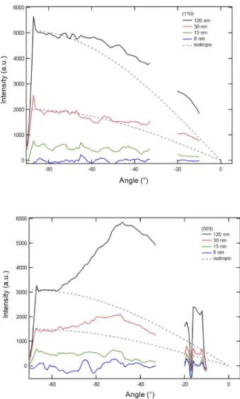
Figure 3.3: (a) Pole figure (sin(!) weighted integral) for the (110) di↵raction feature of P3MT CPB films at 1.2 ˚A 1. Gaps are due to detector structure. Di↵raction intensities are
detected for films 30 nm thick. Dashed lines indicate the expected behaviors of isotropic systems. The 33 and 100 nm thick films exhibit light textures for orientation⇠30 from the surface normal. (b) Pole figure (sin(!) weighted integral) for the (020) di↵raction feature of P3MT CPB films at 1.8 ˚A 1. Di↵raction intensities are detected for films 30 nm thick.