STRUCTURAL PROPERTIES OF COBALT/SILICON THIN FILM AS A
FUNCTION OF DEPOSITED THICKNESS AND ANNEALED
TEMPERATURE
Anil Kumar1, Ranjeet Kumar Brajpuriya2, Sumana Kayal *1
1
Department of Electronics and Communication Engg. , Amity University Haryana, Manesar, India 2
Department of Nanotechnology, Amity University Haryana, Manesar, India
ABSTRACT
The paper presents structural property measurement of Cobalt/silicon thin film as a function of
thickness as well as of annealed at different temperatures. The synthesis of Co/Si thin film is
done by Resistive heating. The structure of the Co/Si interface gets change with increase of
thickness of interface, from amorphous to nano-crystalline. The X-ray diffraction measurement
gives oriented growth of as-deposited Co/Si film in hcp (0 0 2) direction. But the sample
annealed around 400˚C shows the formation of CoSi at the interface. The change in the
structural behaviour is because of certain causes mainly: (i) relaxation of stress, (ii) growing
nature of grain which is indicated by X-ray diffraction (XRD) measurement.
Keywords: XRD, thin film, nano-crystalline, interface, amorphous.
1. Introduction
Interest in the magnetic thin films and their interfaces with semiconductor surfaces has obtained
significant attention in the recent years because of their technological applications like
non-volatile memories and in the developing field of spintronics [1–3]. In addition to this, the
combination of magnetism of the ferromagnetic layer along with the electronic properties of the
underlying substrate gives the opportunities for designing innovative magneto transport devices
in near future. However, the main problem that comes in these devices is the significant
intermixing of semiconductor elements into the overlayer, which results in a drastic decrease of
the magnetization and increase the resistivity of the whole system [4,5]. But on application of
heat treatment the structural properties gets changed because of the significant intermixing of the
effect of heat treatment on structural properties of Co/Si thin film. The present study is, therefore
aimed at investigation of the structural properties of Co/Si thin films as function of thickness and
annealing temperature.
2. Experimental Details
The different thickness of Co/Si thin films was deposited on Silicon substrate using resistive
heating. The deposition was carried out at a base pressure. The deposition rate was kept constant
for each deposition. The structural measurement was done using high angle X-ray diffraction
technique on X-ray diffractometer (Rigaku RINT 2000) using Cu Kα radiation. All the
characterization measurements were carried out at room temperature. To study the structural
changes upon thermal annealing, the as-deposited films were subjected to thermal annealing in a
furnace of the temperature range 100-400˚C in steps of 100˚C for 2 hours. Resistive Heating has
been performed inside Vacuum Box Coater MODEL: BC-300.
3. Results and Discussion
a. Function of Thickness
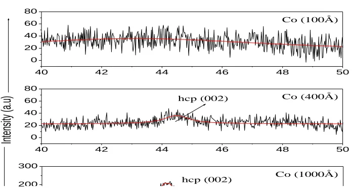
Figure 1 shows the XRD pattern of Co/Si thin film as a function of thickness. The XRD of Co
(100Å) thin film sample shows a broad hump around 2θ value of 44.57˚, as shown in Table 1,
which is the reflection of Co (002) plane. Hence this indicates that the thin film is of an
amorphous in nature. This amorphous nature of the thin film is because of the deposition of
[image:2.612.56.537.543.588.2]lower grain size atom.
Table 1: Work Table for the Cobalt of 100 Å(10nm).
However, XRD pattern recorded on 400 Å, thick Co film shows increase in the intensity of peak
and small shifts towards higher 2θ value. The increase in sharpness of the peak indicates the
increase in grain size of Co thin film and the shift in peak position is due to release of stresses PEAK 2θ Sin2θ 4/3(h2+hk+k2) + l2/(c/a)2 hkl a c d
with increase in the film thickness. It is well known that ultra thin film structures contain various
[image:3.612.170.518.357.545.2]point defects and stresses and they are released as the film becomes more continuous.
Table 2: Work Table for the Cobalt of 400 Å(40nm).
40 42 44 46 48 50
0 100 200 300
hcp (002)
In
ten
sity (a.u
)
2
40 42 44 46 48 50
0 20 40 60 80
40 42 44 46 48 50
0 20 40 60 80
Co (1000Å) Co (400Å) Co (100Å)
hcp (002)
Figure 1: XRD pattern of Co thin films as a function of thickness
However, for 1000 Å thin film sample one can clearly see an intense peak at 2θ = 44.22˚
corresponding to (002) hcp Co as shown in table 3. The obtained 2θ position is consistent with
the value reported for hcp Co. The intense (002) peak shows an amorphous to nano-crystalline
transformation is occurred in Co thin film by surface energy minimization.
PEAK 2θ Sin2θ 4/3(h2+hk+k2) + l2/(c/a)2 hkl a c d
1 41.82 0.12738 1.3504 100 2.490 - 2.1575
Table 3: Work Table for the Cobalt of 1000 Å(100nm).
The average grain sizes calculated using Scherrer formulism [7] as a function of film thickness.
The grain size increases with the film thickness and found to be 7.6 nm for 400Å and 21.04 nm
for 1000Å thick Co/Si film sample.
b. Function of annealing temperature
Fig. 2 shows the XRD patterns of as-deposited as well as annealed Co/Si thin film at different
temperatures. The pattern corresponding to as-deposited film shows the occurrence of sharp peak
at 2θ= 44.68, where the reflection from Co (0 0 2) plane resides.
40 42 44 46 48 50
0 50 100 150
CoSi hcp (002)
4000C/2hr
2
40 42 44 46 48 50
0 25 50 75 100 hcp (002)
Int
en
sit
y (
a.u
)
40 42 44 46 48 50
0 20 40 60 80 hcp (002) 3000 C/2hr 2000 C/2hr
40 42 44 46 48 50
0 20 40 60 80
hcp (002) 1000
C/2hr
40 42 44 46 48 50
0 20 40 60 80
hcp (002) As-deposited
PEAK 2θ Sin2θ 4/3(h2+hk+k2) + l2/(c/a)2 hkl a c d
1 41.12 0.1233 1.3075 100 2.53175 - 2.1926
[image:4.612.126.525.390.655.2]The presence of slight peak around 44.68 indicates the as-deposited sample is mostly
microcrystalline in nature. The obtained 2θ position is consistent with the value reported for hcp
Co [9]. The formation of the pure elemental Co has been seen, hence concluded that solid-state
reaction has not taken place at room temperature while depositing overlayer onto the substrate.
The XRD pattern recorded after 100 ˚C annealing shows a slight shift in the peak towards higher
2θ value along with an increase in peak intensity. Similarly, at 200 ˚C annealing temperature, the
sample follows the same pattern and peak gets intensified along with shifting towards higher
value of 2θ. However XRD pattern recorded at 300 ˚C clearly shows sharp peak and substantial
transformation from microcrystalline to crystalline hcp (002) phase. On increasing temperature
to 400 ˚C peak is shifted towards higher value of 2θ which clearly visible now. The peak is around 2θ=44.82, which shows the reflection of (002) hcp plane. Along with hcp (002) peak
formation, a compound CoSi is formed at 2θ=42.01, which is a reflection of (100) plane. The
formation of CoSi takes place at the interface of the sample.
4. Conclusion
The deposition of different thickness of Co/Si film has been synthesized using resistive heating
technique. Investigation of structural property as a function of thickness has been done. The
grain size increases with the increase in film thickness is been observed by XRD measurement.
Along with thickness, the present work shows the influence of annealing on structural property
of Co/Si thin film.XRD measurements of annealed samples confirm the formation and growth of
CoSi compound at the interface upon annealing at higher temperatures, indicating solid-state
reaction-taking place between the substrate and the overlayer.
References
[1] A. Sharma et al, “Investigation of annealing effects on the structural, magnetic and
transport properties of Co/GaAs (0 0 1) thin films” Applied Surface Science 252(2006)
8571-8575.
[2] D.S. Wang, R.Q. Wu, and A.J. Freeman, “State Tracking First Principles Determination
[3] Datta, S and B. Das, "Electronic analog of the electrooptic modulator". Applied Physics
Letters 56 (1990) 665–667.
[4] J.J. Krebs et al,” Properties of Fe single-crystal films grown on (100)GaAs by
molecular-beam epitaxy” Journal of Applied Physics 61(1987) 2596.
[5] V.P. Labella et al,” Spatially resolved spin-injection probability for gallium arsenide”
Science 292 (2001) 1518.
[6] S. S. P. Parkin, “Origin of enhanced magnetoresistance of magnetic multilayers:
Spin-dependent scattering from magnetic interface states” Phys. Rev. Lett. 71, 1641 _1993_.
[7] C. Scheck et al,” Evolution of interface properties of electrodeposited Ni/GaAs(001)
contacts upon annealing” J. Appl. Phys. 95, 6549 _2004_.
[8] Eberhart J P 1989 Analyse Structurale et Chimiques des Materiaux _Paris: Bordas_.
[9] K.H. Lee et al,” Microstructural properties of Co thin films grown on p-GaAs (1 0 0)