Design of a Low Power Vedic Multiplier using
BKG Reversible Logic Gate
Mayur S M1, Neethu Johny2
1,2
Asst. Professor, Department of Electronics and Communication Engineering, New Horizon College of Engineering, Outer Ring Road, Marathalli, Bengaluru- 560 103
Abstract: This work shows the architecture of low power digital circuits implemented using BKG reversible logic gate. In digital circuits power dissipation can be significantly reduced using reversible logic. It is becoming prominent in applications involving quantum computing and low power applications. BKG is a 4x4 reversible logic gate i.e, it has 4 inputs and 4 outputs out of which 1 input is a ancilla input and 2 out of 4 outputs are garbage outputs. The outputs can be uniquely retrieved from the inputs and vice versa. BKG half adder shows 84.17% reduction in the power consumption when compared to half adder implemented using Feynman and Fredkin reversible gate. It also shows a 79.59% and 25.66% reduction in the power consumption when compared to half adder implemented using MIG and COG reversible gate and Peres reversible logic gate respectively. Since BKG is proved to be better than all the existing reversible logic gates, it is used to implement applications such as encoders and various multipliers.
Keywords: BKG, Ancilla, Garbage outputs, MIG and COG, Peres.
I. INTRODUCTION
Reversible circuits are those circuits which does not lose information. Reversible calculation in a gadget can be executed best while the gadget comprises of reversible doors. These circuits can create particular yield vector from each information vector, and the other way around, i.e, there is a coordinated mapping amongst info and yield vectors. Reversible rationale has gotten exorbitant consideration in the current years because of their ability to diminish the power scattering which is the guideline necessity in low power huge scale mix plan. It has wide uses in low power integral metal-oxide semiconductor and optical science, polymer registering, quantum calculation and nanotechnology. Irreversible equipment working out outcomes in vitality scattering because of information misfortune. Reversible rationale is one of the empowering fields for up and coming low power outline innovations. Since one of the necessities of all advanced flag processors and other hand held gadgets is to diminish control dispersal multipliers with unreasonable speed and lower disseminations are basic.
The rest of the paper is organized as follows. Section II gives the introduction to the full adders implemented using existing reversible logic gates. Section III deals with the proposed full adder architecture using BKG reversible logic gate. Section IV deals with application of the proposed architecture. The results are shown in section V and finally the conclusion is summarized in section VI.
II. EXISTING DESIGN
III.PROPOSED DESIGN
A. BKG Reversible Logic Gate
It is a 4*4 reversible logic gate .The circuit is operated as singly reversible full adder. The full adder is used to design complex adder circuits. This reversible logic gate has low power VLSI design and quantum dot automata .The input vector is represented by T (A, B, C, D) and the output vector is indicated as O (P, Q, R, S). The relation between the output and the input terminals are given by following equations,
P=> A Q=> A^C R=> A^C ^B S=> (A^C) ^B^AC
IV.APPLICATION
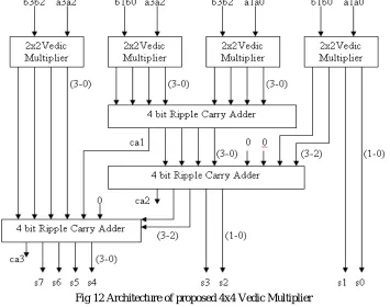
piece multiplier modules. Duplication of the two center 2x2 piece multiplier modules. The second 4-bit RC Adder is utilized to include two 4-bit operands, i.e. connected 4-bit ("00" and most noteworthy two yield bits of right hand the vast majority of 2x2 multiplier module as appeared in Figure 5) and one 4-bit operand we get as the yield entirety of first RC Adder. Its convey "ca1" is sent to third RC Adder. Presently the third 4-bit RC Adder is utilized to include two 4-bit operands, i.e. connected 4 - bit (convey ca1, "0" and most noteworthy two yield entirety bits of second RC Adder) and one 4-bit operand we get as the yield whole of left hand the greater part of 2x2 multiplier module.
Fig 12 Architecture of proposed 4x4 Vedic Multiplier
V. RESULT AND DISCUSSIONS
The proposed 1-bit multiplier is coded in Verilog, simulated using Cadence NC simulator, synthesized using Cadence’s RC encounter and verified for all possible inputs. The simulation inputs are generated using suitable Verilog test bench.
A. Simulation And Synthesis Output
[image:3.612.130.485.160.440.2]The simulation result for 1-bit vedic multiplier is shown in Fig. 9 and the synthesized schematic is shown in Fig. 10.
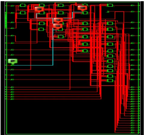
Fig 14 Synthesized schematic of Proposed 4*4 Vedic Multiplier
B. Results And Comparison With Existing Architecture
[image:4.612.172.439.388.518.2]The 1-bit half adder designed is compared with half adders implemented using the existing reversible logic gates in terms of total area and power. The results obtained are tabulated in table 2. From table 2, it is evident that there is a substantial reduction in the parameters.
Table 2 Comparison between existing structures
From the above table it is observed that the BKG half adder shows 84.17% reduction in the power consumption when compared to half adder implemented using Feynman and Fredkin reversible gate. It also shows a 79.59% and 25.66% reduction in the power consumption when compared to half adder implemented using MIG and COG reversible gate and Peres reversible logic gate respectively. It is concluded that the BKG reversible logic gate is efficient compared to all other existing reversible logic gates. Hence the 4*4 Vedic multiplier is then designed using BKG based full adder and Table 3. Results shows the various parameter values.
[image:4.612.190.424.646.708.2]From the above table it is observed that the delay is 3.662ns, the total area occupied is 456 and the total power consumed is 18273.259nW.
VI. CONCLUSIONS
This paper presents a 4x4 Vedic multiplier using BKG based full adders. The paper describes a method to reduce area and power consumption by using reversible logic. The design is implemented using Cadence and the results show less area requirement and low power consumption. The work can further be extended to 8x8, 16x16 multipliers and their comparisons can be studied. The proposed architecture can be used to develop a compact, low power DSP processors, MAC unit.
REFERENCES
[1] Jacob.B.Chacko,Pawan whij, “Low delay based full adder/subtractor by MIG and COG reversible logic gates”, 2016, 8th International conference on
Computational intelligence and communication network.
[2] Landauer, R., “Irreversibility and heat generation in the computing process”, IBM J. Research and Development, 5(3): pp. 183-191, 1961
[3] Bennett, C.H., “Logical reversibility of Computation”, IBM J.Research and Development, 17: pp. 525-532, 1973.
[4] Perkowski, M. And P. Kerntopf, “Reversible Logic. Invited Tutorial” Proc. Euro-Micro, Warsaw, Poland ,Sept 2001.
[5] T. Toffoli, "Reversible computing," in Automata, Languages and Programming, W. de Bakker and J. van Leeuwen, Eds. Springer, 1980, p. 632, technical Memo MIT/LCSITM-151,MIT Lab. For Computer Science.
[6] A. Peres, "Reversible logic and quantum computers", Phys. Rev. A, 32, 1985, pp.3266-3275.
[7] Pradeep Singla, Naveen Kr. Malik," A Cost- Effective Design Of Reversible Programmable Logic Array ", International Journal Of Computer Applications
(0975 – 8887) Volume 41– No.15, March 2012.
[8] “Implementation of Reversible full adder using Peres gate”, International Journal of Engineering research and technology, Vol.3 issue 2, Feb 2013.
[9] R. Feynman, “Quantum Mechanical Computers”, Optical News, Vol. 11, Pp.11-20,1985.
[10] Jagadguru Swami Sri Bharati Krisna Tirthaji Maharaja, “Vedic Mathematics or Sixteen Simple Mathematical Formulae from the Veda, Delhi (1965)”, Motilal
Banarsidas, Varanasi, India, 1986.
[11] M. Morris Mano, “Computer System Architecture”, 3rd edition, Prientice-Hall, New Jersey, USA, pp. 346-348,1993.
[12] H. Thapliyal and H.R Arbania. “A Time-Area-Power Efficient Multiplier and Square Architecture Based On Ancient Indian Vedic Mathematics”, Proceedings
of the 2004, International Conference on VLSI (VLSI’04), Las Vegas, Nevada, pp. 434-9, June 2004
[13] P. D. Chidgupkar and M. T. Karad, “The Implementation of Vedic Algorithms in Digital Signal Processing”, Global J. of Engg. Edu, Vol.8, No.2, 2004 UICEE
Published in Australia.
[14] Thapliyal H. and Srinivas M.B, “High Speed Efficient NxN Bit Parallel Hierarchical Overlay Multiplier Architecture Based on Ancient Indian Vedic
Mathematics”, Transactions on Engineering, Computing and Technology, 2004, Vol.2
[15] Abu Sadat md. Sayem, masashi ueda,” Optimization of reversible sequential circuits” Journal of computing, Vol. 2, No. 6, June 2010, NY, USA, ISSN
2151-9617
[16] Siva Kumar Sastry, Hari Shyam Shroff ,Sk.Noor Mahammad, V. Kamakoti” Efficient Building Blocks for Reversible Sequential Circuit Design”
1-4244-0173-9/06/$20.00©2006IEEE.
[17] E. F. Fredkin and T. Toffoli, "Conservative logic," International Journal of Theoretical Physics, vol. 21, no. 3/4, 1982, pp. 219-253
[18] M. S. Islam, M. M. Rahman, Z. Begum and M. Z. Hafiz, "Low Cost Quantum Realization of Reversible Multiplier Circuit," Information Technology Journal
8(2), 2009, pp.208-213
[19] H. Thapliyal, M.B. Srinivas, "Novel design and reversible logic synthesis of multiplexer based full adder and multipliers", 48th IEEE MIDWEST Symposium