Preparation and Thermal Analysis of Sn-Ag Nano Solders
Tran Thai Bao
1;*1, Yunkyum Kim
1;*1, Joonho Lee
1;*2and Jung-Goo Lee
21Department of Materials Science and Engineering, Korea University, 5 Anam-dong, Seongbuk-gu, Seoul 136-713, Korea
2Functional Materials Division, Korea Institute of Materials Science, 66 Sangnam-dong, Changwon, Gyeongnam 641-010, Korea
In this study, Sn-Ag nano solders of three different compositions (Sn-1.0 mass%Ag, Sn-3.5 mass%Ag and Sn-6.5 mass%Ag) were synthesized via arc-discharge process. The properties of Sn-Ag nano solders were analyzed using X-ray Diffraction (XRD), Transmission Electron Microscopy (TEM), Scanning Electron Microscopy (SEM), Energy Dispersive X-ray spectroscopy (EDX), and Differential Scanning Calorimetry (DSC). Particle size relatively widely ranged from 10 nm to 340 nm. For Sn-1.0 mass%Ag and Sn-3.5 mass%Ag, average size was 200240nm, and that for Sn-6.5 mass%Ag was4050nm with some extra-ordinary large particles of100nm. The melting points of the prepared SnAg nano solders were examined with DSC at different heating rates 1 K, 3 K and 5 K/min. The congruent melting point of Sn-Ag nano solders was found to be 487 K. [doi:10.2320/matertrans.MJ201013]
(Received April 5, 2010; Accepted September 28, 2010; Published November 17, 2010)
Keywords: arc discharge process, differential scanning calorimetry, nano solder, phase diagram, tin-silver alloy
1. Introduction
The melting temperatures of Sn-Ag-Cu and Sn-Cu lead-free solders are in the range between 493 K and 500 K, which are much higher than the melting temperature of conven-tional Sn-Pb solder (approximately 456 K). Accordingly, the solder reflow temperature becomes as high as 533 K.1) In order to decrease the melting point, many attempts have been carried out on new alloy design. However, those attempts have not been so successful. Several researchers paid attention to nanoparticles, because the melting point of nanoparticles can be decreased without changing the chemi-cal composition because of the high surface to volume ratio.1–4) Hsaio and Duh synthesized Sn-3.5 mass%Ag-0.5 mass%Cu nanoparticles at room temperature via chemi-cal reduction method.2)However, without stabilizer, agglom-eration and surface oxidization of the nanoparticles easily occurred, and consequently the melting point of this solder was as high as bulk powder (approximately 489 K). Jiang
et al. used the chemical reduction method to fabricate Sn-3.5 mass%Ag nanoparticle alloy in methanol solution at low temperature using 1.10 phenalthroline as a surfactant. They reported that the melting point of 10 nm Sn-3.5 mass%Ag alloy nanoparticles was decreased by 28.3 K from that of bulk.3) Pande et al. manufactured Sn-3.5 mass%Ag nano-particles in silicon oil at approximately 513 K using ethylene glycol as a stabilizer. The nanoparticles have the average size of (8010) nm and the melting point of 501 K.1)Zouet al. fabricated Sn-3.0 mass%Ag-0.5 mass%Cu nanoparticles us-ing the same method, and decreased the meltus-ing temperature by 4.2 K.4)
The chemical reduction method has been considered as relatively cheap and convenient method to prepare nano solders. However, the chemical reduction method has some problem in reproducibility and difficulties in chemical composition control. Therefore, the chemical reduction method is not suitable for mass production. On the other
hand, the graphite arc process has been used for mass fabrication of nanoparticles. However, this method also has some problems in the particle size control and poor and irreproducible yield. Recently, several researchers applied the arc discharging method as a new preparation method of nano particles.5–8)This convenient method has some unique advantages compared to other methods. Variety systems of binary, ternary, etc. can be easily reproduced with controlled particle size and shape and composition.
Recently, Lee and his co-workers studied the thermody-namic properties of bulk and nano solder alloys.9–16) They calculated the phase diagrams of nanoparticles and pointed out that the melting point decrease may be obtained across the whole composition range for conventional lead-free solder alloys.13)They also found an interesting behavior of the phase diagram of nanoparticles using a simple regular solution model: when the interaction parameter of solid is positive and that of liquid is negative, all the solidus and liquidus lines and the eutectic point move to the corner of the lower melting point component.13) Sn-Ag alloy system at high Sn region have a positive interaction parameter in solid (Sn and Ag3Sn are immiscible in solid), and a negative interaction parameter in liquid.17)Therefore, Sn-Ag system is a good candidate to examine the change in the phase stability of nano system.
In this study, the arc discharge method has been applied for the fabrication of Sn-Ag nano solder alloys. The prepared samples were examined with XRD, SEM, TEM, EDX and DSC. The obtained thermal analysis data were compared with the bulk phase diagram to confirm the decrease in melting temperatures.
2. Experimental
2.1 Sample preparation
Ag (99.99% purity, 1–3 mm grains, Kojundo Chemical Laboratory) and Sn (99.5% purity, 100 mesh powder, Sam Chun Chemicals) were carefully weighed and mixed with different weight percentage of Sn-1.5%Ag, Sn-3.8%Ag and Sn-7.0%Ag respectively. Then master alloy tabulates were
*1Graduate Student, Korea University
prepared with an induction melting furnace in an Ar atmosphere. The solidified samples weighted approximately 220 g (25-mm diameter, 8-mm height).
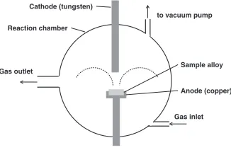
Figure 1 shows a schematic diagram of the arc discharge apparatus. The system consists of a power supply, an arc chamber, a particle collector and a gas circulator. A sample alloy was placed on a water-cooled copper anode plate in the center of the reaction chamber. The upper tungsten rod served as the cathode. The distance between the two electrodes can be controlled from outside during operation. Once a master alloy tabulate was placed at the center of the reaction chamber, it was sealed, evacuated, and introduced Ar gas with a pressure of 20 kPa. The electric voltage and electric current were 20–30 V and 20–90 A, respectively. The arc discharge process was carried out for about 12h, which generated large amount of100g nano powders. The chamber was cooled under Ar gas for 2 h before collecting alloy nanoparticles on the inner surface of the chamber.
2.2 Analysis method
X-Ray Diffraction (18 kW, Rigaku Model D/MAX-2500V XRD) was used to study the crystal structure of SnAg alloy nanoparticles. Transmission Electron Microscope (TEM, Tecnai20, 200 kV), High Resolution Transmission Electron Microscope (HR-TEM, Technai20, 300 kV) and Field Emission Scanning Electron Microscope (FE-SEM, Hitachi S-4300, 30 kV) were used to observe the morphologies of the synthesized nanoparticles. TEM specimens were pre-pared by using ultrasound to disperse manufactured SnAg alloy nanoparticles in ethanol and then one drop of the SnAg alloy nanoparticles solution was placed onto a carbon film supported by copper grids. SEM specimens were prepared as the same way on a silicon wafer. Energy Dispersive X-ray spectroscopy (EDX) (Horiba EX-200) was used to analyze the composition of SnAg nanoparticle alloys. The melting temperature of the nanoparticles alloys were determined by mean of Differential Scanning Calorimetry (DSC). DSC analysis was firstly carefully calibrated with 99.999% purity Sn (Kojundo Chemical Laboratory). For DSC analysis, the nanoparticles were dispersed in alcohol and then the mixture was dropped into an alumina crucible. The analysis was
performed at different heating rates of 1, 3, and 5 K/min in the temperature range of 303 to 623 K under N2 (99.999% purity) atmosphere.
3. Results and Discussion
3.1 EDX study
The compositions of the prepared nanoparticles are given in Table 1. It was found that the Ag concentrations of nanoparticles were slightly lower than that of mother alloys. Nevertheless, the compositions were close to the master alloy, so it is considered that the arc discharge method can fabricate SnAg nano solders with fairly well controlled composition.
3.2 X-ray diffraction (XRD) patterns of SnAg alloys
Figure 2 shows XRD patterns of the SnAg nanoparticle alloys. It is clear that prominent peaks in XRD patterns of SnAg nano alloys are attributed to Sn and Ag3Sn phases. Therefore, it is considered that the Ag3Sn phase was successfully alloyed. From the XRD patterns, oxides peaks were not investigated.
3.3 Transmission electron microscopic (TEM) study
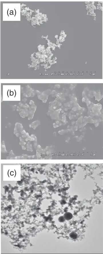
Figure 3 shows the TEM and FE-SEM images of the prepared nanoparticles. From these images, it was found that spherically shaped nanoparticles were partially necked with each other. The observed size distribution of Sn-1.0 mass%Ag nanoparticles was between 80280nm. Few larger particles of approximately 300 nm were also inves-tigated. The particle size distribution of Sn-3.5 mass%Ag was in the range of 100340nm. For these two samples, the average size was 200240nm. For Sn-6.5 mass%Ag alloy nanoparticles, some parts are approximately 100 nm, but most of them were in the range of2080nm (average size was 4050nm). The particle size distribution and weight percentage of all samples were shown in Fig. 4.
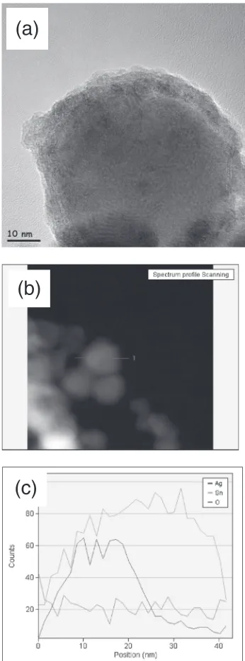
In order to verify the structure of SnAg nanoparticles manufactured by arc discharge process, the line-analysis was carried out. Figure 5 shows the line analysis result of a Sn-6.5 mass%Ag nanoparticle with a HR-TEM image. The Ag peak was only detected in a certain region with the Sn peak in the nanoparticle, which supports the existence of the Ag3Sn phase in the Sn matrix. Accordingly, it is considered that Ag3Sn and Sn phases were simultaneously formed during the arc discharge process. From the HR-TEM image, it is considered that the surface was slightly oxidized, but could not be detected from the line analysis or XRD analysis.
3.4 Differential scanning calorimetry (DSC) study
Figure 6 shows the DSC results with Sn-3.5 mass%Ag samples with three different heating rates. The measured
Cathode (tungsten) Reaction chamber
Gas outlet
Gas inlet to vacuum pump
Sample alloy
Anode (copper)
[image:2.595.48.565.85.128.2]Fig. 1 A schematic illustration of the present experimental apparatus.
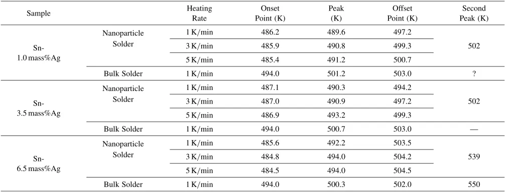
Table 1 Chemical composition of the prepared nanoparticles.
Sample number 1 2 3
Mater alloy Sn-1.5 mass%Ag Sn-3.8 mass%Ag Sn-7.0 mass%Ag
[image:2.595.87.250.157.263.2]onset points (melting starting points) and the second peak points (liquidus temperatures) were almost the same for the three different heating rates. From the DSC analysis result at a heating rate of 1 K/min, it was clearly observed that the main peak was composed of several small peaks. It might be related to the existence of many different sizes of particles, namely as the particle size increased the melting point increased. In addition, during heating, small particles might be coagulated to larger particles. The sequence of coagu-lation of small particles is of interest, but not so easy to investigate. Additional research is required on the coagu-lation in the future work. Nevertheless, the second peak is located on the same position regardless of the heating rate. Therefore, when the particle grew to a certain size, the growth rate was considered to become slower, yielding the same liquidus temperature. Figure 7 shows the DSC
results of the three samples at the same heating rate of 1 K/min. For comparison the DSC results of bulk samples were shown together. The measured melting temperatures of SnAg nanoparticles and bulk alloys were summarized in Table 2.
Using the present experimental results, a schematic phase diagram of Sn-Ag alloy nanoparticles at the Sn-rich corner was visualized in Fig. 8. It is clearly found that the melting point was decreased by67K from the bulk alloy. Mostly interesting result is that for Sn-3.5 mass%Ag nanoparticle a liquidus point was investigated, which was much higher than the bulk eutectic temperature. Therefore, it was expected that the eutectic composition was shifted for nanoparticles. From the phase diagram, it was likely that the eutectic composition was shifted to the Sn rich corner as suggested in our theoretical study.13)
(a)
(b)
(c)
Fig. 3 SEM and TEM images of the prepared nanoparticles: (a) SEM image of Sn-1.0 mass%Ag, (b) SEM image of Sn-3.5 mass%Ag, (c) TEM image of Sn-6.5 mass%Ag.
20 30 40 50 60 70 80
Intensity / a.u.
2
θ
Ag
3Sn
Sn
(a)
20 30 40 50 60 70 80
2
θ
Intensity / a.u.
Ag
3Sn
Sn
(b)
20 30 40 50 60 70 80
Intensity / a.u.
2
θ
Ag
3Sn
Sn
(c)
[image:3.595.336.516.71.516.2] [image:3.595.72.264.75.542.2]4. Conclusions
In the present study, we prepared three Sn-Ag nano solders (1.0, 3.5 and 6.5 mass%) by arc discharge process. The samples were analyzed by XRD, SEM, TEM, EDX and DSC. From the thermal analysis, it was found that the congruent melting point of Sn-Ag nanoparticles was decreased to 487 K. In addition, it was expected that the eutectic composition was shifted to the Sn rich corner.
Acknowledgements
We acknowledges the valuable discussion on DSC analy-sis with Dr. Geun Woo Lee, KRISS. This work was supported by the Korea Research Foundation Grant funded by the Korean Government (KRF-2008-331-D00742).
(a)
(b)
(c)
Fig. 5 (a) HR-TEM image of a Sn-6.5 mass%Ag nanoparticle, and (b), (c) line analysis.
9
Sn3.5Ag 1K/min
7 8
V
Sn3.5Ag
5K/min 3K/min
6 7
ow /
µ
V
5
Heat fl
460 470 480 490 500 510 520 530 540 4
H
460 470 480 490 500 510 520 530 540
Tempertature, T / K
Fig. 6 The DSC curves of Sn-3.5 mass%Ag alloy nanoparticles at different heating rates of 1, 3, and 5 K/min.
40 50
Weight percent (%) Frequency (%)
(c)
30
10 20
Size distribution / %
10 0
Particle size, D/nm
110 100 90 80 70 60 50 40 30 20 30
Frequency (%)
(b)
20
25 Weight percent (%)
5 10 15
100 0
Particle size, D/nm
Size distribution / %
340 320 300 280 260 240 220 200 180 160 140 120 30
Frequency (%)
(a)
20
25 Weight percent (%)
10 15
70 0 5
Particle size, D/nm
Size distribution / %
310 290 270 250 230 210 190 170 150 130 110 90
[image:4.595.339.512.71.537.2] [image:4.595.70.267.73.538.2] [image:4.595.324.528.594.756.2]REFERENCES
1) S. Pande, A. K. Sarkar, M. Basu, S. Jana, A. K. Sinha, S. Sarkar, M. Pradhan, S. Saha, A. Pal and T. Pal: Langmuir24(2008) 8991. 2) L. Hsiao and J. Duh: J. Elect. Mater.35(2006) 1755.
3) H. Jiang, K. Moon, F. Hua and C. P. Wong: Chem. Mater.19(2007) 4482.
4) C. Zou, Y. Gao, B. Yang and Q. Zhai: Mater. Charact.61(2010) 474. 5) T. Watanabe, H. Itoh and Y. Ishii: Thin Solid Films390(2001) 44. 6) D. Y. Geng, Z. D. Zhang, W. S. Zhang, P. Z. Si, X. G. Zhao, W. Liu,
K. Y. Hu, Z. X. Jin and X. P. Song: Scr. Mater.48(2003) 593. 7) X. L. Dong, Z. D. Zhang, S. R. Jin and B. K. Kim: J. Appl. Phys.86
(1999) 6701.
8) X. L. Dong, Z. D. Zhang, Q. F. Xiao, X. G. Zhao, Y. C. Chuang, S. R. Jin and W. M. Sun: J. Mater. Sci.33(1998) 441.
9) J. Lee, T. Tanaka, M. Yamamoto and S. Hara: Mater. Trans.45(2004) 625–629.
10) J. G. Lee, J. Lee, T. Tanaka, H. Mori and K. Penttila: JOM57(2005) 56.
11) J. Lee, T. Tanaka, J. G. Lee and H. Mori: Calphad31(2007) 105. 12) J. Park and J. Lee: Calphad32(2008) 135.
13) J. Lee, J. Park and T. Tanaka: Calphad33(2009) 377.
14) J. G. Lee, J. Lee, T. Tanaka and H. Mori: Nanotechnology20(2009) 475706.
15) T. Kim, J. Lee, Y. Kim, J.-M. Kim and Z. Yuan: Mater. Trans.50 (2009) 2695–2698.
16) H. Xu, Z. Yuan, J. Lee, H. Matsuura and F. Tsukihashi: Colloids Surf. A: Physicochem. Eng. Aspects359(2010) 1.
[image:5.595.66.270.70.250.2]17) H. Ohtani, I. Satoh, M. Miyashita and K. Ishida: Mater. Trans. 42 (2001) 722–731.
Table 2 DSC peaks analysis results of the prepared nanoparticles and bulk alloys.
Sample Heating
Rate
Onset Point (K)
Peak (K)
Offset Point (K)
Second Peak (K)
Nanoparticle 1 K/min 486.2 489.6 497.2
Sn- Solder 3 K/min 485.9 490.8 499.3 502
1.0 mass%Ag 5 K/min 485.4 491.2 500.7
Bulk Solder 1 K/min 494.0 501.2 503.0 ?
Nanoparticle 1 K/min 487.1 490.3 494.2
Sn- Solder 3 K/min 487.0 490.9 497.2 502
3.5 mass%Ag 5 K/min 486.9 493.2 499.3
Bulk Solder 1 K/min 494.0 500.7 503.0 —
Nanoparticle 1 K/min 485.6 492.2 503.5
Sn- Solder 3 K/min 484.8 494.0 504.2 539
6.5 mass%Ag 5 K/min 484.5 494.0 504.5
Bulk Solder 1 K/min 494.0 500.3 502.0 550
560 570
Bulk
540 550
550
Nano solder Bulk
520
530 539
490 500 510
494 494 502
502
0 1 2 3 4 5 6 7 8
480 490
T
e
mperature, T / K
494
487 486
486 487
0 1 2 3 4 5 6 7 8
wt% Ag
Fig. 8 A schematic illustration of the phase diagram of Sn-Ag system. (solid lines: bulk phase diagram, dashed lines: nano phase diagram)
Onset Point: 494K Offset Point: 502K
V
(c)
Liquidus Point: 539K Onset Point: 485.6K Offset Point: 503.5K
Liquidus Point: 550K
µ
V
(b) Onset Point: 494 K Offset Point: 503KH
Liquidus Point: 502K Offset Point: 494.2K
Onset Point: 487.1K
Onset Point: 494K Offset Point: 503K (a)
Heat flow /
Liquidus Point: 502K Offset Point: 494.2K
Onset Point: 487.1K
Nano Solders Bulk
460
Temperature, T / K
Bulk
550 540 530 520 510 500 490 480 470
[image:5.595.321.530.73.235.2] [image:5.595.46.549.321.514.2]