Growth Behavior of Au–Sn and Ag–Sn Compounds
during Solid-state Reactive Diffusion between Au–Ag Alloys and Sn
Toshio Takenaka
1;*1, Satoru Kano
1;1, Masanori Kajihara
1;*2,
Noriharu Kurokawa
2and Katsuhiko Sakamoto
21Department of Materials Science and Engineering, Tokyo Institute of Technology, Yokohama 226-8502, Japan
2Tyco Electronics AMP Co., Ltd., Kawasaki 214-8533, Japan
The kinetics of the solid-state reactive diffusion between binary Au–Ag alloys and Sn was experimentally examined using Sn/ Au0:75Ag0:25/Sn and Sn/Au0:5Ag0:5/Sn diffusion couples. The diffusion couples were prepared by a diffusion bonding technique and then
isothermally annealed at temperatures ofT¼393, 433 and 473 K for various times up to 1272 h in an oil bath with silicone oil. Under the present experimental conditions, AuSn4and AuSn2compound layers were observed after annealing. Furthermore, fine particles of Ag3Sn were rather
uniformly distributed in the Au–Sn compound layers. The total thicknesslof the Au–Sn compound layers is expressed as a power function of the annealing timetas follows:l¼kðt=t0Þn, wheret0is unit time, 1 s. Here, the exponent takes values ofn¼0:34{0:40. The mean interdistancerof
the Ag3Sn particles is also described as a power function oft:r¼krðt=t0Þp, wherep¼0:28{0:43. Assuming that the interdistancervaries in
proportion to the grain size of the Au–Ag compound during annealing, the rate-controlling process of the reactive diffusion was estimated. If the grain boundary diffusion across the Au–Sn compound layers is the only rate-controlling process, the values ofncalculated from the equation
n¼ ð1pÞ=2become smaller than the experimental values ofn¼0:34{0:40. Consequently, both the volume diffusion and the grain boundary diffusion should contribute to the rate-controlling process of the reactive diffusion.
(Received April 11, 2005; Accepted June 21, 2005; Published August 15, 2005)
Keywords: diffusion bonding, intermetallic compounds, bulk diffusion, solder, gold–silver–tin system
1. Introduction
In electronic industry, Sn-base solder alloys are widely used to interconnect Cu-base conductor alloys. However, Cu–Sn compounds are formed at the interface between the conductor and solder alloys due to soldering and then grow continuously during energization heating under usual service
conditions.1–9)Since such compounds are brittle and possess
high electrical resistivities, their growth deteriorates the electrical and mechanical properties of the interconnection. Most of Cu-base conductor alloys are plated with Au to improve the corrosion resistance. When the Au-plated conductor alloy is in contact with the Sn-base solder alloy mechanically, the ductility and the electrical conductivity of the conductor alloy at the mechanical contact considerably degenerate owing to usual energization heating. Such degeneration is ascribable to the formation of Au–Sn compounds at the mechanical contact due to the reactive
diffusion between Au and Sn at solid-state temperatures.10–12)
The solid-state reactive diffusion was experimentally
studied by the present authors for the binary Au–Sn,10–12)
Ag–Sn13)and Cu–Sn14)systems. In those experiments, Sn/
Au/Sn, Sn/Ag/Sn and Sn/Cu/Sn diffusion couples with sandwich construction were prepared by a diffusion bonding technique and then annealed at various temperatures in an oil
bath. In the case of the Au–Sn system, AuSn4, AuSn2 and
AuSn compound layers were observed to form at the Au/Sn interface in the diffusion couple at annealing temperatures of
T ¼393{473K. The total thickness of the Au–Sn compound
layers is mathematically expressed as a power function of the annealing time, and the exponent of the power function takes
values of 0.48, 0.42 and 0.36 at T ¼393, 433 and 473 K,
respectively.11,12)If the reactive diffusion is controlled by the volume diffusion of the constituent elements in each phase, the exponent is equal to 0.5. On the contrary, the grain boundary diffusion across the compound layer will govern the reactive diffusion at low temperatures where the volume diffusion is frozen out. When the reactive diffusion is purely controlled by the grain boundary diffusion and grain growth takes place in the compound layer according to the parabolic
law, the exponent becomes 0.25.15)Here, the parabolic law
means that the grain size of the compound layer is propor-tional to the square root of the annealing time. In the Au–Sn
system, the exponent is equal to 0.36 at T ¼473K and
increases with decreasing annealing temperature. At
T ¼393K, it becomes close to 0.5. The value of 0.36 yields
that the grain boundary diffusion contributes to the rate-controlling process and the grain growth occurs at a certain
rate atT ¼473K. However, atT¼393K, the grain growth
will decelerate, though the contribution of the grain boundary diffusion becomes more conspicuous. When the grain growth is very stagnant, the volume fraction of grain boundaries with a finite thickness remains almost constant, and hence the effective cross-section for the grain boundary diffusion scarcely varies during annealing. In such a case, the exponent becomes nearly equal to 0.5, even if the reactive diffusion is purely controlled by the grain boundary diffusion. This is the
reason why the exponent is smaller than 0.5 atT¼473and
433 K but close to 0.5 at T ¼393K in the Au–Sn
system.11,12)Such temperature dependence of the exponent
was observed also for the Ag–Sn system,13)but the reverse
temperature dependence was recognized for the Cu–Sn system.14)
Binary Au–Ag alloys are used as corrosion-resistant conductor materials in electronic industry. In the binary
Au–Ag system,16)the complete solid solution phase with the
face-centered cubic (f.c.c.) structure appears at a wide *1Graduate Student, Tokyo Institute of Technology
*2Corresponding author, E-mail: [email protected]
temperature range. If the Au–Ag conductor alloy is mechan-ically contacted with the Sn-base solder alloy and then heated at solid-state temperatures under energization conditions, Au–Sn and Ag–Sn compounds can be formed at the mechanical contact. Such formation may also cause degen-eration of the electrical and mechanical properties of the conductor alloy. However, experimental information on the coinstantaneous formation of the Au–Sn and Ag–Sn com-pounds under such conditions is limited. Recently, the reactive diffusion between Sn and a binary Au–Ag alloy was
experimentally observed by the present authors.17) In that
experiment, a Au–25 at %Ag alloy was sandwiched between
pure Sn, and then annealed atT ¼433K for various times in
the oil bath. Due to annealing, the AuSn4 and AuSn2
compound layers are produced at the interface in the Sn/ (Au–Ag)/Sn diffusion couple. Furthermore, fine particles of
Ag3Sn are distributed rather uniformly in the Au–Sn
compound layers. In order to examine the kinetics of the coinstantaneous growth of the Au–Sn and Ag–Sn compounds under energization heating conditions, the solid-state reactive diffusion between Au–Ag alloys and Sn was observed more extensively in the present study. Sn/(Au–Ag)/Sn diffusion couples were prepared by the diffusion bonding technique using pure Sn and binary Au–25 at %Ag and Au–50 at %Ag
alloys and then annealed at temperatures between T ¼393
and 473 K. The layer growth of the Au–Sn compounds was observed metallographically. The observation was carried out also for the grain growth of the Ag–Sn compound. On the basis of the observations, the rate-controlling process of the reactive diffusion will be discussed.
2. Experimental
Binary Au–Ag alloys with Ag concentrations of 25 and 50 at % were prepared as 25 g button ingots by argon arc melting from pure Au and Ag with purity of 99.99%. Plate
specimens with a size of 10mm5mm2mm were cut
from the ingot and cold rolled to a thickness of 0.1 mm. Sheet
specimens with a dimension of 20mm7mm0:1mm
were cut from the plate specimen and then chemically polished in an etchant composed of 20 vol % of hydrochloric acid, 10 vol % of nitric acid and 70 vol % of distilled water. The chemically polished sheet specimens were separately annealed in evacuated silica capsules at 1223 K for 2 h, followed by air cooling without breaking the capsules. The annealed sheet specimens were again chemically polished in the etchant mentioned above.
Pure Sn plate specimens with a size of12mm5mm
2mm were prepared by cold rolling and spark erosion from a
commercial 1 kg rectangular ingot of pure Sn with purity of 99.99%. The cold-rolled plate specimens were separately annealed in evacuated silica capsules at 473 K for 2 h, followed by air cooling without breaking the capsules. The annealed Sn plate specimens were chemically polished in an etchant consisting of 20 vol % of hydrochloric acid, 20 vol % of nitric acid and 60 vol % of distilled water. The two
surfaces with an area of 12mm5mm of each Sn plate
specimen were mechanically polished on 1000 emery paper. One of the two polished surfaces was again mechanically
polished on 1500–4000 emery papers until a depth of 100mm
and then finished using diamond with a diameter of 1mm.
After chemical polishing, a Au–Ag sheet specimen was immediately sandwiched between the finished surfaces of two freshly prepared Sn plate specimens in methanol by a
technique used in previous studies.10–14)The Sn/(Au–Ag)/Sn
couples were completely dried and then heat treated for
diffusion bonding in an oil bath with silicone oil atT ¼393,
433 and 473 K for 72, 24 and 6 h, respectively. After the heat
treatment, the diffusion couples were annealed atT ¼393,
433 and 473 K for various times up to 1200 h. The summation of the heat-treating and annealing times is hereafter merely called the annealing time. Cross-sections of the annealed diffusion couples were mechanically polished using diamond
with diameters of 15, 3 and 1mmand then finished with an
OP-S liquid by Struers Ltd. The microstructure of the cross-section was observed with a back-scattered electron image (BEI) by scanning electron microscopy (SEM). Concentra-tions of Au, Ag and Sn in each phase on the cross-section were measured by electron probe microanalysis (EPMA).
3. Results and Discussion
3.1 Microstructure
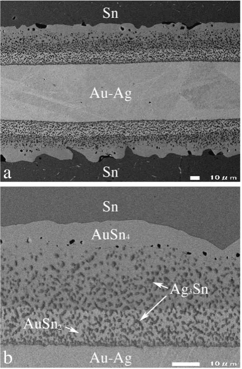
Typical BEI micrographs for the cross-section of the
Au0:5Ag0:5 diffusion couple annealed at T ¼433K for
t¼72h (2:59105s) are shown in Fig. 1. Here, t is the
annealing time. For simplicity, the type of diffusion couple is
denoted by the composition Auð1yÞAgyof the Au–Ag alloy
in the diffusion couple, whereyis the mol fraction of Ag. As
can be seen in Fig. 1(a), compound layers with slightly different contrasts are observed to form at the (Au–Ag)/Sn interface. In such compound layers, fine particles with the most dark contrast are distributed rather uniformly. In order to identify each phase, concentrations of Au, Ag and Sn were measured by EPMA. According to the measurements, the compound layer with a more dark contrast on the Sn specimen side is AuSn4, that with a less dark contrast on the
Au–Ag alloy side is AuSn2, and the fine particle with the
most dark contrast in the AuSn4and AuSn2layers is Ag3Sn.
The solubility of Au in the Ag3Sn phase and those of Ag in
the AuSn4 and AuSn2 phases are less than 1 at %.
Further-more, fine particles are spottily dispersed in the Sn specimen.
These particles are the AuSn4 phase precipitated during air
cooling after annealing.11,12)The Au–Ag compound layers in
the diffusion couple of Fig. 1(a) are magnified in Fig. 1(b). Although no Ag3Sn particle is recognized in the region of the
AuSn4layer on the Sn specimen side, the mean grain size of
the Ag3Sn particles is almost equivalent in the AuSn4 and
AuSn2 layers.
As already mentioned in Introduction, the AuSn4, AuSn2
and AuSn layers are produced in the Au1Ag0diffusion couple
at T ¼393{473K.10–12) However, the AuSn layer was not
clearly recognized in the Au0:75Ag0:25 and Au0:5Ag0:5
diffusion couples at the same temperatures. If we look at the micrograph in Fig. 1(b) carefully, we may find that a very thin layer with a slightly dark contrast exists along the
interface between the AuSn2layer and the Au–Ag alloy. This
very thin layer may be the AuSn compound. Under the present annealing conditions, however, the AuSn layer does not grow to thicknesses enough to determine the composition
by EPMA accurately. On the other hand, in the Au0Ag1
diffusion couple, the Ag3Sn and layers are formed at
T ¼433{473K.13)However, only the Ag
3Sn compound was
observed in the Au0:75Ag0:25 and Au0:5Ag0:5 diffusion
couples at T ¼393{473K. According to a recent phase
diagram in the ternary Au–Ag–Sn system,18)the Ag3Sn phase
is in equilibrium with the Sn, AuSn4, AuSn2, AuSn and
phases at T ¼479K. At this temperature, however, the
phase is not in equilibrium with the Sn, AuSn4 and AuSn2
phases. Such phase equilibria will be realized also at
T ¼393{473K. Consequently, the Ag3Sn phase appears in
the AuSn4 and AuSn2layers but not thephase.
3.2 Growth behavior of intermetallic layer
As mentioned earlier, the AuSn4 and AuSn2 layers are
observed in the BEI micrograph of the cross-section like
Fig. 1. Thus, from the BEI micrograph, the total thicknessl
of the Au–Sn compound layers was evaluated at each annealing time as follows:
l¼A=w: ð1Þ
Here,wandAare the total length parallel to the interface and the total area of the Au–Sn compound layers, respectively, on
the cross-section. The results atT ¼393, 433 and 473 K are
plotted as open triangles, squares and circles, respectively, in Fig. 2. In this figure, the ordinate indicates the logarithm of
the thicknessl, and the abscissa shows the logarithm of the
annealing timet. Figures 2(a) and (b) indicate the results for the Au0:75Ag0:25 and Au0:5Ag0:5 diffusion couples,
respec-tively. For convenience sake, the layer consisting of the
AuSn4 and AuSn2 compounds is hereafter called the
intermetallic layer. As can be seen in Fig. 2, the thicknessl
of the intermetallic layer monotonically increases with
increasing annealing time t. The plotted points at each
temperature are located well on a straight line. This means
that the thicknessl is mathematically expressed as a power
function of the annealing timetby the equation
l¼kðt=t0Þn: ð2Þ
Here,t0 is unit time, 1 s. It is adopted to make the ratiot=t0
dimensionless. The proportionality coefficientkhas the same
dimension as the thickness l, but the exponent n is
dimensionless. From the plotted points in Fig. 2, the values
Fig. 1 Back-scattered electron images of cross-section for the Au0:5Ag0:5
diffusion couple annealed at 433 K for 72 h (2:59105s).
Fig. 2 The thicknesslof the intermetallic layer versus the annealing timet
at temperatures of 393, 433 and 473 K for the (a) Au0:75Ag0:25 and (b)
Au0:5Ag0:5diffusion couples. Straight lines indicate the calculations from
[image:3.595.318.532.72.475.2] [image:3.595.48.291.73.444.2]ofkandnwere determined by the least-squares method. The
determination gives k¼1:5107m andn¼0:40at T¼
393K, k¼6:2107m and n¼0:36 at T¼433K and
k¼8:4107m andn¼0:40atT ¼473K for the Au
0:75
-Ag0:25diffusion couple, andk¼2:0107m andn¼0:36
atT¼393K,k¼3:1107m andn¼0:40atT¼433K
and k¼2:0106m and n¼0:34 at T ¼473K for the
Au0:5Ag0:5 diffusion couple. Using these values ofkandn,
the thicknesslwas calculated as a function of the annealing
timetfrom eq. (2). The results atT¼393, 433 and 473 K are shown as dotted, dashed and solid lines, respectively, in Fig. 2.
As already mentioned in Introduction, the solid-state reactive diffusion was experimentally studied by the present
authors for the binary Au–Sn10–12) and Ag–Sn13) systems
using the Au1Ag0and Au0Ag1diffusion couples,
respective-ly. The AuSn4, AuSn2 and AuSn layers are formed in the
Au1Ag0diffusion couple at T¼393{473K, and the Ag3Sn
andlayers are produced in the Au0Ag1diffusion couple at
T ¼433{473K. The experimental results of the total
thick-nesslversus the annealing timetfor the Au1Ag0and Au0Ag1
diffusion couples are shown as open circles and rhombuses, respectively, in Fig. 3. Also in this figure, the ordinate
indicates the logarithm of l, and the abscissa shows the
logarithm of t. Figures 3(a) and (b) indicate the results at
T ¼433and 473 K, respectively. In this figure, the plotted
points in Figs. 2(a) and (b) are also represented as open squares and triangles, respectively. At each annealing time,
the thickness is almost equivalent among the Au1Ag0,
Au0:75Ag0:25 and Au0:5Ag0:5 diffusion couples but about
one order of magnitude greater for these diffusion couples
than for the Au0Ag1 diffusion couple. This means that the
growth rate of the Au–Sn intermetallic layer is rather insensitive to the composition of the Au–Ag alloy in the diffusion couple under the present experimental conditions. Consequently, it is concluded that the degeneration of the mechanical and electrical properties at the interface between the Au–Ag conductor and Sn-base solder alloys due to the formation of the Au–Sn compounds occurs at almost the same rate as the interface between pure Au and the Sn-base solder alloy under usual energization heating conditions.
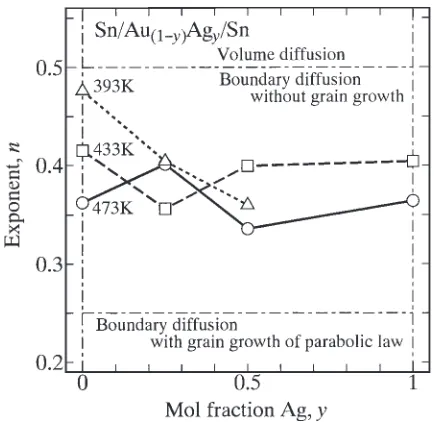
The values of the exponentn atT¼393, 433 and 473 K
are plotted against the composition y as open triangles,
squares and circles, respectively, in Fig. 4. Here, the ordinate
and the abscissa indicate n and y, respectively. As can be
seen, nis close to 0.5 at y¼0 andT ¼393K. Except this
plotted point, however,ntakes values between 0.34 and 0.42.
As already mentioned in Introduction, the values ofnsmaller
than 0.5 are realized only by the combination of the occurrence of the grain growth and the contribution of the grain boundary diffusion to the rate-controlling process. The results in Fig. 4 indicate that such combination is practically actualized in most of the diffusion couples under the present annealing conditions.
Fig. 3 The thicknesslof the intermetallic layer versus the annealing timet. The results for the Au0:75Ag0:25and Au0:5Ag0:5diffusion couples in Fig. 2
are represented as open squares and triangles, respectively, at temperatures of (a) 433 and (b) 473 K. The corresponding results for the Au1Ag011,12)
and Au0Ag113)diffusion couples are shown as open circles and rhombuses,
respectively. Straight lines indicate the calculations from eq. (2).
Fig. 4 The exponentnversus the mol fractionyof Ag at temperatures of 393, 433 and 473 K.
[image:4.595.62.279.297.716.2] [image:4.595.318.535.546.757.2]3.3 Grain growth in intermetallic layer
Under the present experimental conditions, fine particles of Ag3Sn are rather uniformly distributed in the intermetallic
layer. Hence, the mean interdistancerof the Ag3Sn particles
in the intermetallic layer on the cross-section was evaluated by the equation
r¼ ða=cÞ0:5: ð3Þ
Here,ais the area of the intermetallic layer distributed with the Ag3Sn particles on the cross-section, andcis the number
of the Ag3Sn particles in the areaa. The results atT ¼393,
433 and 473 K are plotted as open triangles, squares and circles, respectively, in Fig. 5. In this figure, the ordinate
shows the logarithm of the interdistancer, and the abscissa
indicates the logarithm of the annealing timet. Figures 5(a)
and (b) show the results for the Au0:75Ag0:25 and Au0:5Ag0:5
diffusion couples, respectively. As can be seen, the
inter-distancermonotonically increases with increasing annealing
timet. If the interdistanceris mathematically described as a
power function of the annealing timetby the equation
r¼krðt=t0Þp; ð4Þ
the following values of the proportionality coefficientkrand
the exponent pare obtained from the plotted points in Fig. 5
by the least-squares method: kr¼1:4108m and p¼
0:36atT ¼393K,kr¼1:3108m and p¼0:43atT ¼
433K andkr¼9:4108m andp¼0:33atT¼473K for
the Au0:75Ag0:25diffusion couple; andkr ¼1:0108m and
p¼0:35atT ¼393K,kr¼3:4108m and p¼0:33at
T ¼433K andkr¼1:6107m andp¼0:28atT¼473
K for the Au0:5Ag0:5diffusion couple. Using these values of
kr andp, the interdistancerwas calculated as a function of
the annealing timetfrom eq. (4). The results atT ¼393, 433 and 473 K are shown as dotted, dashed and solid lines, respectively, in Fig. 5.
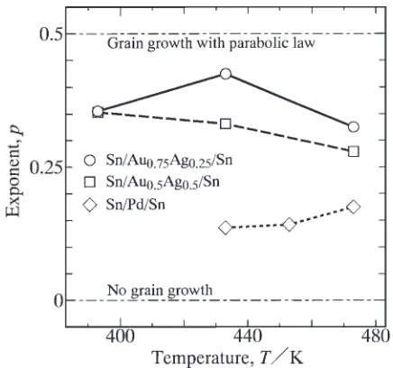
The values of p for the Au0:75Ag0:25 and Au0:5Ag0:5
diffusion couples are plotted against the annealing
temper-atureT as open circles and squares, respectively, in Fig. 6.
Here, the ordinate and the abscissa indicate p and T,
respectively. Recently, the solid-sate reactive diffusion
between Pd and Sn was experimentally studied at T ¼
433{473K using Sn/Pd/Sn diffusion couples by the present
authors.19) At the interface in the diffusion couple, PdSn
4,
PdSn3 and PdSn2 layers were observed at T ¼433K, but
only PdSn4 and PdSn3 layers were recognized at T¼453
and 473 K. Unlike the Au–Sn intermetallic layer, however, grain boundaries were discerned clearly in the Pd–Sn
intermetallic layer. Thus, the mean grain size g of the Pd–
Sn intermetallic layer could be determined experimentally.
According to the experimental results, the grain size g is
expressed as a power function of the annealing time t:
g¼kgðt=t0Þp. The values of p for the Pd–Sn intermetallic
layer are shown as open rhombuses in Fig. 6. As can be seen,
pis much greater for the Au–Sn intermetallic layer than for
the Pd–Sn intermetallic layer. Although the relationship
between the interdistancerand the grain sizegis not known
for the Au–Sn intermetallic layer, r should be a monotone
Fig. 5 The interdistancerof the Ag3Sn particles versus the annealing time
tat temperatures of 393, 433 and 473 K for the (a) Au0:75Ag0:25and (b)
Au0:5Ag0:5diffusion couples. Straight lines indicate the calculations from
eq. (4).
Fig. 6 The exponent p versus the annealing temperature T for the Au0:75Ag0:25and Au0:5Ag0:5diffusion couples. The corresponding results
[image:5.595.61.275.326.736.2] [image:5.595.317.535.542.746.2]increasing function of g. Therefore, the results in Fig. 6 imply that the grain growth occurs more remarkably in the Au–Sn intermetallic layer than in the Pd–Sn intermetallic layer.
3.4 Grain growth of Ag3Sn particle
Assuming that the shape of the Ag3Sn particle in the
intermetallic layer is the sphere with a constant diameter ofd,
we evaluate the mean size s of the Ag3Sn particle on the
cross-section by the equation
s¼2ðb=Þ0:5: ð5Þ
Here,bis the mean value for the area of each Ag3Sn particle
intersected by the cross-section. Furthermore, there exists the
following relationship between the mean size s and the
diameterd:
ðs=2Þ2d¼ ðd=2Þ34=3; ð6Þ
and hence we obtain the equation
d¼sð3=2Þ0:5: ð7Þ
The mean areab was determined from the BEI micrograph
like Fig. 1, and then the diameter d was estimated from
eqs. (5) and (7). The results atT ¼393, 433 and 473 K are
plotted as open triangles, squares and circles, respectively, in Fig. 7. In this figure, the ordinate and the abscissa show the logarithms ofd andt, respectively. Figure 7(a) indicates the results for the Au0:75Ag0:25 diffusion couple, and Fig. 7(b)
shows those for the Au0:5Ag0:5 diffusion couple. As can be
seen, the diameterdmonotonically increases with increasing
annealing timet. Whendis expressed as a power function of
tby the equation
d¼kdðt=t0Þm; ð8Þ
the following values ofkdandmare obtained from the plotted
points in Fig. 7 by the least-squares method: kd ¼6:9
109m andm¼0:35atT ¼393K,kd ¼2:9108m and
m¼0:32atT ¼433K andkd ¼7:0108m andp¼0:30
at T ¼473K for the Au0:75Ag0:25 diffusion couple; and
kd¼1:0108m andm¼0:32atT ¼393K, kd ¼1:8
108m andm¼0:35at T¼433K andkd¼5:2108m
and m¼0:36 at T ¼473K for the Au0:5Ag0:5 diffusion
couple. Using these values ofkdandm,dwas calculated as a
function oft from eq. (8). The results atT¼393, 433 and
473 K are shown as dotted, dashed and solid lines, respec-tively, in Fig. 7.
The values of m for the Au0:75Ag0:25 and Au0:5Ag0:5
diffusion couples are plotted against the annealing
temper-atureT as open circles and squares, respectively, in Fig. 8.
Here, the ordinate and the abscissa indicate m and T,
respectively. As can be seen, m is close to 1/3 for all the
plotted points. Hence, at first glance, the grain growth of the
Ag3Sn particle seems to take place according to the Ostwald
ripening.20)However, the total volume of the Ag3Sn particle
monotonically increases with increasing annealing time during the reactive diffusion. Consequently, the grain growth
of the Ag3Sn particle cannot be described with a simple
coarsening model. Nevertheless, the results in Fig. 8 imply
Fig. 7 The diameterdof the Ag3Sn particle versus the annealing timetat
temperatures of 393, 433 and 473 K for the (a) Au0:75Ag0:25 and (b)
Au0:5Ag0:5diffusion couples. Straight lines indicate the calculations from
eq. (8).
Fig. 8 The exponent m versus the annealing temperature T for the Au0:75Ag0:25and Au0:5Ag0:5diffusion couples.
[image:6.595.62.275.69.479.2] [image:6.595.316.535.70.274.2]that a coarsening process similar to the Ostwald ripening works in the Au–Sn intermetallic layer.
3.5 Rate-controlling process
As already mentioned in Section 3.3, the relationship
between the grain sizegof the Au–Sn intermetallic layer and
the interdistance r of the Ag3Sn particle is not known.
However,rshould be a monotone increasing function ofg.
Assuming that r is proportional to g, the rate-controlling
process for the growth of the Au–Sn intermetallic layer was estimated. When the growth is purely controlled by the grain boundary diffusion across the intermetallic layer, the follow-ing relationship15)holds good between the exponentsnandp.
n¼ ð1pÞ=2 ð9Þ
The values ofncalculated from eq. (9) for the Au0:75Ag0:25
and Au0:5Ag0:5 diffusion couples are plotted against the
annealing temperature T as open circles and squares,
respectively, connected with dashed lines in Fig. 9. In this figure, open circles and squares connected with solid lines show the experimental values ofn for the Au0:75Ag0:25 and
Au0:5Ag0:5diffusion couples, respectively, in Fig. 4. As can
be seen in Fig. 9, most of the calculated values are smaller than the corresponding experimental values. This means that eq. (9) overestimates the contribution of the grain boundary diffusion to the rate-controlling process. Consequently, it is concluded that the growth of the Au–Sn intermetallic layer is controlled by both the volume diffusion and the grain boundary diffusion and the grain growth occurs at certain rates in the intermetallic layer.
4. Conclusions
The solid-state reactive diffusion between binary Au–Ag alloys and Sn was experimentally studied using the Sn/
Au0:75Ag0:25/Sn and Sn/Au0:5Ag0:5/Sn diffusion couples
prepared by the diffusion bonding technique. The diffusion couples were isothermally annealed at temperatures between
T ¼393 and 473 K for various times in the oil bath with
silicone oil. Due to annealing, the AuSn4 and AuSn2
compound layers are formed at the (Au–Ag)/Sn interface in the diffusion couple. Furthermore, the fine particles of
Ag3Sn are rather uniformly distributed in the Au–Sn
compound layers. The total thickness l of the Au–Sn
compound layers monotonically increases with increasing annealing timetaccording to the equationl¼kðt=t0Þn, where
t0 is unit time, 1 s. For the Sn/Au0:75Ag0:25/Sn diffusion
couple,k¼1:5107,6:2107and8:4107m atT ¼
393, 433 and 473 K, respectively, and n¼0:40, 0.36 and
0.40 atT ¼393, 433 and 473 K, respectively. On the other
hand,k¼2:0107,3:1107 and2:0106m atT ¼
393, 433 and 473 K, respectively, and n¼0:36, 0.40 and
0.34 at T ¼393, 433 and 473 K, respectively, for the Sn/
Au0:5Ag0:5/Sn diffusion couple. The mean interdistancerof
the Ag3Sn particles in the Au–Sn compound layers is also
expressed as a power function oftas follows:r¼krðt=t0Þp.
For the Sn/Au0:75Ag0:25/Sn diffusion couple, kr¼1:4
108m and p¼0:36atT ¼393K,kr¼1:3108m and
p¼0:43atT¼433K, andkr¼9:4108m andp¼0:33
atT ¼473K. On the contrary,kr ¼1:0108m and p¼
0:35atT ¼393K,kr¼3:4108m and p¼0:33atT ¼
433K, andkr¼1:6107m andp¼0:28atT ¼473K for
the Sn/Au0:5Ag0:5/Sn diffusion couple. If the interdistancer
is proportional to the grain sizegfor the Au–Sn compound
layers, the exponent p represents also the annealing time
dependence ofg. Assuming that the grain boundary diffusion
across the Au–Sn compound layers is the only
rate-control-ling process, the exponentn is estimated from the equation
n¼ ð1pÞ=2.15)However, most of the estimated values are
smaller than the corresponding experimental values. This means that the reactive diffusion should be controlled by both the volume diffusion and the grain boundary diffusion.
Acknowledgements
The present study was supported by Tyco Electronics AMP Co., Ltd., Japan. The study was also partially supported by a Grant-in-Aid for Scientific Research from the Ministry of Education, Culture, Sports, Science and Technology of Japan.
REFERENCES
1) L. Zakraysek: Welding Research Supplement Nov. (1972) 536–541. 2) K. N. Tu: Acta Metall.21(1973) 347–354.
3) H. N. Keller: IEEE Trans. Components, Hybrids, Manuf. Tech. CHMT-2 (1979) 180–195.
4) H. N. Keller and J. M. Morabito: Surf. Interface Anal.3(1981) 16–22. 5) J. O. G. Parent, D. D. L. Chung and I. M. Bernstein: J. Mater. Sci.23
(1988) 2564–2572.
6) A. J. Sunwoo, J. W. Morris, Jr. and G. K. Lucey, Jr.: Metall. Trans.23A
(1992) 1323–1332.
7) P. T. Vianco, P. F. Hlava and A. L. Kilgo: J. Electron. Mater.23(1994) 583–594.
8) D. R. Frear and P. T. Vianco: Metall. Trans.25A(1994) 1509–1523. 9) S. Choi, T. R. Bieler, J. P. Lucas and K. N. Subramanian: J. Electron.
Mater.28(1999) 1209–1215. Fig. 9 The exponentnversus the annealing temperatureT. The values ofn
for the Au0:75Ag0:25and Au0:5Ag0:5diffusion couples in Fig. 4 are plotted
[image:7.595.63.277.70.280.2]10) M. Kajihara, T. Yamada, K. Miura, N. Kurokawa and K. Sakamoto: Netsushori43(2003) 297–298.
11) T. Yamada, K. Miura, M. Kajihara, N. Kurokawa and K. Sakamoto: J. Mater. Sci.39(2004) 2327–2334.
12) T. Yamada, K. Miura, M. Kajihara, N. Kurokawa and K. Sakamoto: Mater. Sci. Eng. A390(2005) 118–126.
13) K. Suzuki, S. Kano, M. Kajihara, N. Kurokawa and K. Sakamoto: Mater. Trans.46(2005) 969–973.
14) T. Takenaka, S. Kano, M. Kajihara, N. Kurokawa and K. Sakamoto: Mater. Sci. Eng. A396(2005) 115–123.
15) Y. L. Corcoran, A. H. King, N. de Lanerolle and B. Kim: J. Electron. Mater.19(1990) 1177–1183.
16) T. B. Massalski, H. Okamoto, P. R. Subramanian and L. Kacprzak: Binary Alloy Phase Diagram (ASM International, Materials Park, OH, 1990) vol. 1, p. 12.
17) S. Kano: Master Eng. Thesis, Tokyo Institute of Technology, 2003. 18) P. Villars, A. Prince and H. Okamoto: Handbook of Ternary Alloy
Phase Diagrams (ASM International, Materials Park, OH, 1995) vol. 3, p. 2170.
19) T. Takenaka, M. Kajihara, N. Kurokawa and K. Sakamoto: Mater. Sci. Eng. A, in press.
20) R. Wagner, R. Kampmann and P. W. Voorhees: in Phase Trans-formations in Materials, ed. G. Kostorz (Wiley-Vch Verlag GmbH, Weinheim, 2001), pp. 370–373.