Automatic Location
Of
IC
Design
Errors Using
An
E-beam
System
H.Pelgara'. M.Battu'',
P.Garino',J.Lhme*. Y.J.Vernays.
Y.Marzouki',
F.Boland61.
CSELT
-Via Reiss Romoli 274, 10148 Torino. Italy. 2.BTRL
-
Ipswich, M o l k . I F 5?RE.
United Kingdom.3.
CNET-
Chemin du Vieux Chene. B.P. 98, 38249 Meylan, France4. MAG/TlM3 - 46 Avenue FelixViallet, 38031 Grenoble, France
5.
"DU
-Department of Microelectronics, Dublin 2. Ireland.Abstract
YLSa
validation task relieves on the use of E-beam equipment. However, the lacking of a strong connectionhetreen the CAD (Computer Aided Design) world and the E- Beam world has somehow reduced the powerfulness of this technique. The
ADVICE
System', is an enhanced CAD linked E-beam tester to locate automatically des@ emors on custom VISI devices. The goal is met by building a set of new procedures to drive the interactive electron beamdebugging
(EBD)
spBtem according to the strategies devised by the algorithms based on Fault Dictionarg/ Hierarchical Probing Algorithm mixed search.1. Introduction
E-beam based IC debugging systems are gaining more and more importance, due to VLSI evolution. I t is well known the importance of the use of E-beam microscopes for contact-less probing of the internal nodes of VLSI circuits without disturbing or even destroying the chip [l-31.
However, only in the last couple of years was it felt necessary to move the E-beam experience from the world of the physicist t o the world of the integrated circuit (IC) designers [4]. This migration increased the need t o integrate the
CAD
data and the E-beam system into one unit. Some commercial systems are appearing on the market [5]: they provide the E-beam user with a CAD linked friendly environment that makes it easy to display and search the IC electrical netlist and layout description and t o select nodes to be probed. The EBT control is performed by a remote workstation. However. up to now, the system has not been suitable for automatic debugging, since each logical node is associated with a full electrical track on the layout rather than to preselected test points. Furthermore, the finepositioning on the track has had to be performed by hand.
*) The research has been carried out in the Esprit Project 271:ADVICE, Automatic Design Validation of Integrated Circuit using &beam, partially funded by ;be European Economic Community, Contractors being CSELT-
In this paper the
ADVICE
fully automatic E-beamdiagnostic system will be introduced, strongly integrated with the design environment and providing a user-friendly interactive environment for assisted debugging. A relevant capability of the system is performing the automatic fault location task, starting from IC simulation and mask data.
Section ( 2 ) will briefly describe the ADVICE system, while Section (3) will introduce the fully automatic approach. In order to allow complete automation, some easy des* fw
E-beam debugging (EBD) r u l e s and some test generation and simulation strategies (Section 4) should be followed. Background knowledge about the circuit behaviour is derived from fault simulation and represented in the Fault Dictionaries (Section 5). Finally, the automatic diagnostic process will be described in Section ( 6 ) by outlining the algorithms devoted t o the probe point selection.
2 Draft description of the
ADVICE
SystemThe overall goal of ADVICE is to provide the design/test engineer with an interactive, user friendly environment, integrated with the design environment, to perform all the debugging procedures in a computer assisted/aided way [ 7 ] .
As a novel aspect of the project, the integration between design data and the test environment plays a pre- eminent role: design data is used to make the debugging process as automatic as possible (identication of physical co-ordinates on the chip for beam placement
[a]
starting both from layout information and node names used in high level description, layout pattern recognition to perform accurate positioning of the beam [9], comparison of physical measures against simulation results [ 10-111 and a n automatic probe algorithm).The interaction between the user and the system is aided by giving a working environment which puts, at the designers finger tips, all information related to the device
It&'
under debug (layout information, netlists, aimulation/measure results, fault dictionary and so on): it consists of a graphical multi-window, multi-menu driven
program, that will provide the user with an interactive environment [ 7 ] . The information is displayed using the layout window, the SEM control windows, the waveform display window. Furthermore a text and command window gives a link to the facilities of the workstation operating system to perform test pattern editing. background simulation, fault dictionary processing, user assisted diegnosis
...
In the past the problem of locating the beam exactly on the appropriate nodes was solved manually: the user had to look for the points to be tested on the plot of the IC, then to find them again on the SEM screen by moving the DUT. During a debugging session, a lot of points are measured and normally the obtained SEM images do not satisfactorily help the positioning on the tracks (e.g. in stroboscopic mode).
As
a consequence, the completely manual way of working ishardly feasible.
The probe positioning task can be sketched in four steps by using the CAD information:
Identiflcation of the signal name to be tested, starting from the logical level description:
Retrieval of the probing point on the layout repre sentation;
Positioning using stepper motors (coarse placement): Checking the correctness of the positioning and adjustment, if necessary (fine placement) using pattern recognition.
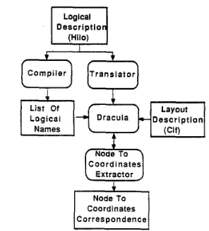
The f i s t two steps are tightly coupled, and are based the extraction of information collected off-line: the association between a signal name (at the logical level) and its corresponding probing point coordinates on the layout representation (see figure 1). Hence automatic positioning can be achieved simply specifying the logical name.
The third step is performed by converting the previous coordinates into drive signals for the stepper motors. The last step involves pattern recognition techniques; it can be
powerfully faced using an automatic pattern recognition tool [S][lZ] by matching the two images obtained from the SEA4 (as a result of step 3) and the CAD layout window data centered around the measuring point, deriving the offset to
be applied to the beam.
The ADVICE System is integrated on a Vaxstation II/GPX. The beam placement can be also achieved by using a module which allows the user to explore the CAD layout data exploiting the circuit hierarchy, retrieving (given a logical
Logical Descriptio
Compiler Translator
00
List Of Layout
Logical
(Cif)
[image:2.622.348.496.71.234.2]Node To Coordinates Correspondence
Figure 1: Node-to-coordinate correlation procedure
name, as mentioned above) or extracting a test point and converting the CAD coordinates of it into commands that drive the stepper motors.
Once the point is located, measurement can be performed using a signal averager [lo]. The system offers several features to display and to manipulate the waveforms, t o filter and to threshold them in order to reduce the noise and to obtain. logic levels: this allows the engineer to easily handle the results obtained. The acquired waveforms can also be compared against logic/analogue simulation results.
All the operations concerning the SEM are concentrated in a unique environment (the Vaxstation) by means of specific modules [Is]: they control parameters l i e magnification, astimatism, scan rotation and focus
adjustments.
The integration of the previous described modules leads to an assisted debugging environment depicted in figure. 2. Considering the sequence of operation normally performed during a debugging session, a flow can be outlined, as in figure 3. This flow can be interpreted both as an assisted and an automatic procedure by substituting the "Determine next node" box with the probing algorithm described in next sections.
3. The fully automatic system
Section 2. has depicted the interactive ADVICE system. The final goal of the project is to demonstrate the feasibility of a fully automatic system, that tries to lighten the load of the user from the highly interactive tasks like the selection of next probing point, the comparison against the simulation results and the decision as to whether the fault has actually
'"'""'](-)
simulat. network7
1
2
%
d r i v e r s
display
- / I
sem sem
I
ate1
1
(dut)H
controlQ u r e 2: User assisted ADVICE System
START
I
I
Test generation & logic simulationI
Translate to test languageI
I
Download to tester LSEM based station)
1
I I
I
Test device (top level, uses I/O pins)
I
I
Initialize the E-beam tester1
I
pindow CAD data around next node to test1
r
Move to auuroximate co-ordinatesP
I
I .r I I
[Obtain an imam of :he area around node
I
I
1
Determine and am& beam correctionI
I
II
Get the waveformII
I
Compress the waveform III
I
I
I
Compare with expected responseI
x r . -
I
I
Is fault located?
I cs
N n
-
.-1
<Track thoroughly checked? I[Back to start using next hierarchical levell
Q u r e 3: ADVICE System operation flow
'""](-)
r e s u l t s descript.'4"!*---*<f
diction.process
lavout
a t e diaanos. imaae d r i v e r s tasks recogniz.
- U
-Fwure 4 Fully automatic ADVICE System
The user can also use the automatic system as an expert advisor, acting in a computer assisted debugging environment.
The achievement of this goal has required f i s t the definition of general strategies on IC design techniques, to make them E-beam debuggable. Afterwards, the problems of the logical description of the chip, the test pattern generation and its simulation, together with the collection of information about the fault free and the faulty behaviour, had to b e faced.
The diagnostic tasks, starting from the knowledge about the logical model and the layout of the circuit, simulation results and the status of the debugging procedure, selects the point to be probed, compare the measured and the simulated waveforms and try to locate the failing area of the IC.
High importance is also given to the user interaction: a quite extensive set of commands (68 basic commands,
divided in 5 classes) is provided to the user t o dialogue with the system, to navigate into the diagnosis data structure, to drive the search or only t o get reports from the automatic search procedures.
The following sections will describe both the design/simulation strategies and the developed procedures.
4. Design and simulation strategies for EHD
The user place (see figure 2) is taken by the Diagnosis The complexity of VLSI circuits, together with their Tasks (figure 4). The automatic system is built as a master h u h degree sequential logic, creates great problems in process able to control the previously described interactive verifying the design correctness. EBT techniques can create, system: all the interactive system capabilities can be to next generation devices, new constraints more rigid than
In order to overcome these problems, three sets of rules have been defined [ 141:
*
logical design rules;*
topographical rules;*
probing point selection rules.These rules provide IC designers, untrained in SEY techniques, with a memorandum on the way of preparing their design in order to make E-beam debugging more easily achievable. Logical and topographical design rules do not introduce too strong constraints to the designer, but provide suggestions on the way in which classical DFT rules must be applied. Probing point selection rules are adopted in the procedure to automatically derive probing point coordinates
(see figure I).
The background knowledge about the circuit under debug is represented by the I C layout, the IC logical description, the test patterns applied and the circuit fault- free and faulty results. As it was previously mentioned in Section 2, the correlation between the layout and the logical naming convention is necessary to achieve an automatic placement of the SEM stage.
Some guidelines must be suggested to solve the following problems. related to fault free simulation process:
(1) how to describe the circuit; (2) how t o generate test patterns; (3) how to capture the simulation results.
As
for point (1). some recommendation can be issued to the designer in order to exploit the inherent I C hierarchy during the debugging sessions.The Hilo-3 simulator [15] has been selected as a common simulation environment within the ADVICE project. The IC logical description, the test patterns, the simulation
results and the fault dictionary a r e derived from the Hilo-3 interface formats.
The designer should build up the circuit description, following its functional hierarchy, highlighting in this way the functional block partitioning. Each functional block, at least at the higher levels, should have a correspondence to a physical block the routing wires among sub-circuits should have physical pendants. Those lines should be accessible on the device. Probing points should be provided at least a t the physical output node (where the signal is generated) and at
each fan-out branch (where the signal is seen as an input).
The kernel of the diagnostic task is represented by a hierarchical data structure, built up compiling the logical
description. This data structure contains also all diagnosis related information, as it w i l l be described in the sequel, step by step.
Many probing points are common to different hierarchy levels. To avoid redundancies and time lost searching the layout data, a list is built, called the SyLonyn L i s t all ZogkaUy equivalent nodes point to a single element in the list.
Definition 1: Two nodes are logically equivalent if they are the branch-free connection between a lower level cell and the boundary of the higher level cell including it.
If there is a fan-out branch, the two nodes are no longer equivalent, since a logical cut can compromise the behaviour. Each element in the Synonym list is associated to a Probing Point List, including the physical probing co-
ordinates and the coded results of the measures. Furthermore, for each logically equivalent node set, a linked list of pointers t o the eq2lipDtentiaUy c o m e e t a d s e t is kept. De6uition 2 Two nodes are equipotentially connected if they are directly connected by a wire.
A netlist tracing procedure, working bottom-up, is built t o determine, for each cell port, at any hierarchical level, the signal propagation direction. Cell ports are distinguished among: input, output and potentially bidirectional.
Delhition 3: A cell port is said potentially bidirectional if on both cell sides (externally and internally) the port sees data sources and destinations.
Port bidirectiondity is said only potential. since it is analysed statically, without taking into account the effect of signals controlling the data sources.
For each cell port, at each level of hierarchy a l i t of
logical dependency is built.
Definition 4:One input and one output, belonging to the same cell, are logically dependent if a path can be traced in the internal network that connects them.
In this data structure, a list of logically dependent inputs is built for each output in the cell header and for each output, a list of logically dependent inputs is provided. This structure is very important to optimise the hierarchical tracing procedures during the diagnostic tasks.
Figure 5 shows a network described using the hierarchy: it is composed by nested blocks. When tine b
C a--
gates 1 and 2 the three stems are equipotentially connected, but not logically equivalent. Line 1 is logically dependent from e (a) and f (g), while f controls l and m.
E-
l B
m
2
f'B
b--
2
9
I
All the previously listed information are extracted from the netlist. Furthermore, the input file to the node-to- coordinate correspondence generator, listing the logically equivalent node set. is automatically generated. The node- to-coordinate correspondence file is loaded in the Synonym List: all E-beam unobservable nodes (i.e. all nodes for which a probing point was not found) are deleted from the Synonim List, since they cannot provide direct contribution to the diagnosis. The user can decide to substitute the deleted nodes with the Nearest f3servation Node.
Definition 5: Node j is said the Nearest Observation Point of node i if j is the nearest observable node controlled by i. Note
that i and j can be a t different hierarchical levels.
The adopted design strategies, based on functional partitioning for debugging, should allow a "Divide and Conquer" test generation method. A test sequence, for each functional block will be off-line generated and simulated. This approach, aiming to exercise a single block at a time, makes test generation easier, and reduces the area to be scanned during diagnostic process, focusing the search mainly on the target functional block.
Each test pattern is composed by sub-sequences built following the "Start Small" approach try to affect small parts of the block not yet tested, to reduce the diagnostic ambiguity. This approach was selected to get a large reliance on the information derived from the device pins: if a faulty behaviour is associated to many failure candidates, many measures with the SEM must be performed, loosing time and disturbing the chip.
Each sub-sequence is normally composed of
-
-
the reset part (possibly absent) to be repeated only once: the homing part (possibly absent) to be repeated eachthe test sequence, to be repeated each loop. loop;
-
The off-line, fault-free sirnulation is performed for each input pattern, saving the logical information about all
E-
beam obsemble nodes, included in the Synonim List after its pruning (to delete unobservable nodes). The list of nodes t o be captured is automatically generated. The user can select the target block to be simulated and the maximum hierarchical level of nodes to be saved, t o reduce the simulation report files.The user should provide to the ADVICE system a very
compacted fde specifying, for each pattern, the target block under test, start and stop time for "loopable sequences". simulation report file names. This file, called H i s t o r y File is used by the diagnostic procedures to select the test pattern t o be applied at any diagnosis step.
The circuit logical description, the aforementioned data structures, the History File and the captured logical information represent the back-ground knowledge about the fault-free circuit. They willbe used as the Golden hit for the automatic diagnostic procedures. However, some pre- computed knowledge about the possible faulty behaviours of the device can be useful to speed up the diagnostic tasks.
5. Fault dictionary generation strategies
In the design environment, fault simulation of the circuit is performed to validate the computed test sequences against a defhed set of faults. The parameters normally collected are the fault coverage (percentage of detected faults, over the total fault set) and the list of undetected faults. Furthermore: only collapsed faults are considered during the fault simulation process; a fault is dropped after the Brst detection (SOFE: Stop On First Error technique).
When failure diagnosis must be performed, the information derived from a careful fault simulation can, in many cases, shorten dramatically the t i m e needed to locate the trouble on the chip.
The analysis of the faulty behaviour is performed by the Hilo-3 fault simulator. The fault sets assumed are stuck-at-
0/1. open line. shorts between lines. Faults can be injected either on the E-beam observable wires only, or also on net whose nearest observation point has been identified.
Though fault collapsing is performed, to speed up the
simulation process, a list of the faults belonging to a collapsed class is kept.
The fault behaviour information is summarised in a Fault Dictionary (FD). Since the procedure of building up a
Ales can be very large, the subsequent debugging tasks must be capable of handling different levels of exhaustive
information.
For each sub-pattern, two FD levels can be built:
(1) include all faults, assuming as observation points the
(2) consider only the faults in the target block, assuming as circuit primary outputs;
observation points the cell outputs.
The first level is intended for the external detection of
errors (observing the output pins with a logic analyser), taking into account the side effects of the test pattern on the other blocks. Level (2) is used for internal detection by the SEM. It is also intended to evaluate very peculiar patterns, developed for internal observation, without considering the fault effect propagation to the primary outputs.
Both levels are built with SOFE technique within each sub-pattern, to exploit the inherent sequential structure of the sub-pattern. However, the same technique cannot be applied to the full pattern sequence, since no temporal relationship can be guaranteed about the sub-pattern; they could be applied in any chronological order.
The command file to inject the fault in a fault simulation session is automatically generated by the system, according to the selected fault models and the target block and the primary observation points specified.
The previously described FD represents the F h d t y
Behaviour Background Knowledge that should allow a reduction in the number of measurements needed to perform the diagnostic tasks and the amount of on-line computation needed to locate the failure site.
6. The diagnostic tasks: the probing algorithm
Previous sections have shown how the adoption of some rules and some strategies can make the diagnostic task of VLSI feasible. Many algorithms were developed to locate faulty devices in printed circuit boards (PCB's). Some of them were based on ad hoc written diagnostic procedures, for each particular PCB which helped the operator in moving the probe to a predefined measure point. Other techniques were based on the analysis of given signatures and comparisons against results contained in a fault dictionary.
The
ADVICE
system, starting from the previous diagnostic experiences in the PCB world, tries to derive them in the IC and E-beam world, providing a set of tools able to carry out the debug process either fully automatically, or to assist the user's work.The "a priori" knowledge is represented by the Golden
&it Model, composed by the hierarchical circuit description, the test pattern, the simulation results and the
Faulty Unit Models. mainly the fault dictionaries. The diagnostic tasks, starting from this information, exploit the circuit hierarchy, aiming to optimise the following cost functions:
-
-
-
-
amount of computations.number of
SEM
measures to be performed; number of test patterns to be applied;amount of searches in the fault dictionaries;
The diagnostic tasks must face the problem that the
back-ground information can be provided at different levels of exhaustivity. One of the advantages of this approach is that, the diagnostic procedures can detect a misbehaviour, although it was not considered at the fault dictionary generation phase, since they act with the Difference Fhdt
Model. Design errors can be hardly mapped in simple stuck- at fault models, since, having partially excluded wrong logic synthesis, verified comparing the layout with the logical description, the other errors are mainly timing errors.
Furthermore, the cost of an exhaustive fault simulation of all possible errors is not acceptable.
The diagnostic tasks see the interactive ADVICE system as procedures able to interface them t o the physical reality. The main procedures called are (figure 4):
-
theCAD
data loader;-
the ATE drivers (loader/down-loader):-
the SEM control procedures (parameter settling, stage control, acquisition system):the E-beam fine positioning system (based on image recogniser).
-
The user interacts with the diagnostic tasks and with the external procedures through the LXugnostiC Task Shell
(figure 6). Lots of commands (68 basic commands, subdivided in five classes: system commands, file oriented commands, set commands, show commands, execution commands) are provided to the user to load the description, create the different command files, select strategies, set values in the data structure, navigate into the hierarchical description, perform debugging operations or monitor the work of automatic procedures.
The diagnostic tasks can be subdivided into two classes:
reconstruct.
I I I
I I 1 '
Flgure 6 Diagnostic tasks interconnection
Class (1) is composed of
The test pattern selector: given the target block, it selects the next sub-pattern to be applied and transfers it to the ATE drivers.
The comparator: it compares the simulated results with either the pattern derived from the logic analyser, or the digital waveform extracted from the SEM measured signal; it provides the temporal information about the differences. A comparison timing tolerance can be specified to cope with simulation or measure inaccuracy.
The logical value reconstructor: given an internal cell, at any hierarchical level, it performs its logical simulation, assuming as stimuli the measured input waveforms; it compare the simulated output against the measured ones, looking for discrepancies.
Fault dictionary navigation procedure: given a measured sub-pattern, it looks for fault candidates; given a fault, it searches all sub-patterns that could have detected it.
The second class is composed of the procedures that perform the selection of next target cell or next probing point. The diagnostic tasks start their job when the ADVICE
system has already been loaded with back-ground information about the circuit and the SEM has already been initialised.
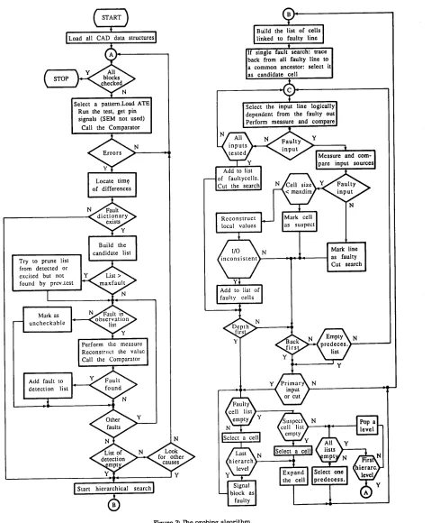
Faure 7 provides a flowchart of the sequence of operations performed during a debugging session, describing the implemented probing algorithm. A detailed description can be found in
[le].
The algorithm starts from the top view of the circuit description, selects a block not yet tested, selects the
developed pattern, performs a test on the primary output. If
the responses are found wrong, looks into the fault dictionary if some simulated fault can generate such wrong behaviour. If the list of fault is longer than the selected threshold, it tries to prune the set of the candidates, excluding those fault that should have been detected by the previous patterns, and performs the measures into the fault
sites.
If no faults included in the fault dictionary can provoke the observed wrong values, or no error i s found in the candidate fault sites, the probing algorithm starts analysing the network structure, from the faulty primary output, backwards looking for a candidate faulty block. When the block is found, the procedure goes down one level of
description hierarchy, trying to locate defendant sub-cells.
The procedure stops when either a connection or a leaf cell have been found to be faulty.
It must be noted that, by exploiting the description hierarchy, no time is lost to analyse in detail not faulty cells. Furthermore, no redundant measures are performed, since the probing points are associated to each element in the Synonym List, rather to each possible logical name: each performed measure result (existence, time and error value) i s stored to avoid measure repetition.
The user can drive the diagnostic procedures by tuning some parameters. They are mainly the number of faults, derived from the FD considered acceptable for direct probing; the size of the cell for which the logical value reconstructor is used.
Three search strategies, used to build the list of candidate cells, have been implemented, to cope with different chip architectures or debugging methods. They are:
-
back first;-
depthfist;-
breadth Arst.The first one traces through the network until a cell with only correct inputs is found. This is useful for single fault hypothesis, and a poorly interconnected network.
The second one, when a suspected cell is found, goes deep into its hierarchy, trying to locate the failure site in it.
The third one tries to build an error frontier, by considering all the cells connected to the previous target one, before going further in the trace-back procedure. This strategy can be applied to tree structures, aiming to adopt
the heuristic of looking for a common ancestor as a next target cell, skipping some cells. Furthermore it can be useful to build a draft map of defendant cells, during a 6rst
(-)
Load all CAD data structures
5=
blocks
Run the test, get pin signals (SEM not used)
Errors
c-
Locate timeof differences
Build the candidate list Try to prune list
from detected or excited but not found by prev.test
-4
-Mark as
uncheckable list
Reconstract the valuc
Add fault to detection list
I
Start hierarchical search
5
=
l
Build the list of cells linked to faulty line
back from all faulty line to a common ancestor: select it as candidate cell
Select the input line logically dependent from the faulty out Perform measure and compare
L
i n p u t s tested
i n p u t
F p e l
local valuesI
inconsistent
Add to list of
4
faulty cellsMark line as faulty Cut search
[image:8.614.87.566.62.642.2]y-w
* L r S t predeces.The diagnostic tasks try to mimic the operation performed by a skillful user, taking advantage of the back- ground knowledge. The user should tune system parameters and select strategies to improve the system behaviour. The procedures can work with different levels of deduced information, and provide different diagnostic strategies. The user can also use the probing algorithms and the fault dictionary navigation procedures as advisors, that can help
him in the IC debugging job.
7. conclusions
The evolutions in SEM technology has made the
adoption of the E-beam probing technique both necessary and feasible to achieve VLSI design validation.
This paper has introduced an integrated assisted- automatic design validation environment based on an SEM- workstation system connected to the CAD world. The ADVICE system provides the user with a "no knobs" SEN equipment, together with all the facilities for logical and electrical IC validation that he is accustomed to use in the design area.
The research work is being carried out within the Esprit Project No.271, ADVICE, which started in November 1984 and will last until October 1989.
Up to now, no EBT system either commercially mailable or even announced provides a fully automatic VLSI validation environment. The systems recently described in literature [6] cannot cope with industrial requirements. Other systems like [17] seem to be more oriented to combinational logic diagnosis, and shows the drawback of
working with images rather than with waveform (too long
measure time to get accurate timing evolutions). The absence of available results in literature gives an idea of the research inherent complexity.
The ADVICE system at present delivered can provide full automation of the SEM. under the workstation control and the link to the CAD world.
The research on the fully automatic diagnostic tasks is under development. System, procedure definition and Diagnostic Task Shell development are completed, while the final system is foreseen by the beginning of '89. First results on prototype tools have provided encouraging responses. The adopted strategy, based on the integration between fault dictionary based techniques and probing algorithm driven
search seems to cope well with the need of keeping Fault Dictionary size and EBT measure time small. The work to be
performed during next year is on one side devoted to ameliorate the diagnostic procedures, on the other side to make the full ADVICE system transferrable to other
companies, since a clear interest has been demonstrated by some EBT companies in commercially exploiting the ADVICE results, before the end of the project.
The authors would like t o acknowledge Mr. M.Cocito
(CSELT) for his work of middleman, having been the project leader, Mr. G.Proctor (BTRL) for his hot encouragements and his guidance, F.Stentiford, T.Twell and LWhyte
(BTRL),
Mr. B.Courtois and LGuiguet (IMAG), for their indispensable contributes to the research development. Finally we intend t o thank Mr. D.Ranasinghe and Mr. D.Machi (BTRL), Mr. G. Ghigo and G.Bestente (CSELT) for their useful work in ameliorating the E-beam system.BibIiography
E.Wolfgang, RLinder, P.Fazekas, H.Feuerbaum: "Electron beam testing of
VLSI
circuits", IEEE Trans. on Electr. Dev., vol. ED-26, N.4, April '79, pp. 549-559. E.Menze1, E.Kubalek "Electron beam test system for VLSI circuit inspection", Scanning Electron Microscopy, 1979, vol. 1, pp. 297-304.M. Cocito, D.Soldani: "Evaluation of performances of a commercial E-beam testing system", Scanning Electron Microscopy, 1983. vol. 1, pp. 45-54.
L.Berger, J.Laurent, B.Courtois, J.P.Collins: "Towards automatic failure analysis of complex ICs through
E-
beam testing", International Test Conference 1986, pp. 465-471.S.Concina, G.Liu, LLattanzi. KReyfman, N.Richardson: "Software integration in a workstation-based E-beam tester", International Test Conference 1986, pp. 644- 649.
T.Tamama, ?I.Kuji: "Automatic fault diagnostic EB tester and its application to a 40K-gate V I S I circuit", International Test Conference 1985, pp. 643-649.
M.Cocito, M. Melgara: "ADVICE: A European effort", 1st Europ. Conf. on Elect and Opt. beam testing of IC, 1987, invited paper, these proceedings.
M.G.Battu', G.A.Bestente, P.G.Cremonese, kB.Di Janni, P.A.Garino: "Automatic positioning for electron beam probing", XI Int. Congr. on Electron Microscopy, 1986, pp. 651-652.
FStentiford, T.Tviel1: "Automatic registration of scanning electron microscope images", 1st Europ. Conf. on Elect. and Opt. Beam Testing of IC, 1987. these proceedmgs.
[ll] F.Boland, P.Linch "Analysis of the stroboscopic mode",
1st Europ. C o d . on Elect. and Opt. Beam Testing of IC, 1987, these proceedings.
[12] LGuiguet, D.Micollet, J.Laurent, B.Courtois: "Electron beam observability and controllablity for the debugging of integrated circuits", MI Europ. Solid State Circuit Conf. 1986, pp. 181-183.
[13] D.W.Ranasinghe, GProctor, M.Cocito, G.Bestente: "Computer control of Electron beam testing for design validation of VLSI circuits", XI Int. Congr. on Electron Microscopy, 1986. pp. 619-620.
[14] M.Melgara, B.Courtois, M.Marzouki, D.Micollet Y.J.Yernay: "Design for electron beam debugging", ADVICE deliverable report, June 87.
[15] Hilo-3 User manual, Copyright 1985, GenRad
Inc.,
[l6] M.Melgara: "The ADVICE probing algorithm definition",
[17] T.Yano, H.Okamoto: "Fast fault diagnostic method using fault dictionary for electron beam tester", International Test Conference 1987, pp. 561-565.
Milpitas, CA, USA