RESEARCH ARTICLE
PROPERTIES OF ZNS BUFFER LAYER PREPARED BY CBD FOR SOLAR CELLS
1*Kavitha, M.
2Gopinathan, C.,
3Chandramohan, R. and
1Pandi, P.
1
Department of Physics, The Madura College, Madurai – 11 Tamilnadu, India
2
Department of Solar Energy, School of Energy Sciences, Madurai Kamaraj University, Madurai – 21,
Tamilnadu India
3
Department of Physics, Sree Sevugan Annamalai College, Devakottai-630303, Tamilnadu, India
ARTICLE INFO ABSTRACT
Zinc sulfide thin films have been deposited onto glass substrates by chemical bath deposition. Thin films of ZnS with different thicknesses of 720nm to 1045 nm were calculated from UV parameters. The effect of film thickness on structural and electrical properties was studied. The thermal conductivity of ZnS thin film is 0.88W/K-m. The structural and activation energy studies support this decrease in the resistivity due to improvement in crystallinity of the films which would increase the charge carrier mobility and decrease in defect levels with increase in the thickness of film. Aim of the work is analyzed the particle structure by X-ray Diffraction (XRD), surface morphology Scanning Electron Microscopy (SEM) and optical properties by UV-Visible spectroscopy and thermal conductivity ZnS thin films. The result indicates that the conductivity of the buffer layer is generated the carriers with minimal losses while coupling light to the junction with minimum absorption losses, yields a highly efficient solar cell.
Copyright © Kavitha, et al., This is an open access article distributed under the Creative Commons Attribution License, which permits unrestricted use, distribution, and reproduction in any medium, provided the original work is properly cited.
INTRODUCTION
Recent investigations have evoked considerable interest in ZnS thin films due to their vast potential for use in thin film devices. Zinc sulfide has found wide use as a thin film coating in the optical and microelectronic industries. ZnS thin films are very useful in the applications such as solar selecting decorative coatings, UV light emitting diode, photo catalyst in flat panel displays, photo electrochemical and solar cell applications. There are many techniques can be used to prepare ZnS films which including electrode position (Lokhande et al., 1998), pulsed-laser deposition (Yano et al., 2003), RF reactive sputtering (Shao et al., 2003), atomic layer epitaxy (Oikkonen
et al., 1998) and chemical bath deposition method (Yamaguchi et al., 2003). Among these techniques, the chemical bath
deposition method is considered as very common technique. It is found to be a cheap and simple way to deposit large area polycrystalline metal chalcogenide thin films. The preparation of various thin films using chemical bath deposition technique such as NiSe (Anuar et al., 2010), SnS2 (Li et al., 2011), CdS (Kim et al., 2010), CdSe (Gopakumar et al., 2010), In2S3 (Asenjo et al., 2010), NiS (Anuar et al., 2011), Cd1-xZnxSe (Hankare et al., 2006) and CdSSe (Ezema et al., 2007) have reported by several authors. In this paper Zinc sulfide thin films have been deposited onto glass substrates by chemical bath deposition.
*Corresponding author: Kavitha, M.
Department of Physics, The Madura College, Madurai–11 Tamilnadu, India
The various deposition parameters such as volume of sulfide and acetate ion source, pH of bath, deposition time, temperature etc are optimized. Thin films of ZnS with different thicknesses of 44nm to 48nm were prepared by changing the bath parameters. The effect of film thickness on structural and electrical properties was studied. The thermal conductivity of ZnS material is almost similar of .82W/K-m. The structural and activation energy studies support this decrease in the resistivity due to improvement in crystallinity of the films which would increase the charge carrier mobility and decrease in defect levels with increase in the thickness of film. Aim of the work is analyzed the particle structure by X-ray Diffraction (XRD), surface morphology Scanning Electron Microscopy (SEM) and optical properties by UV-Visible spectroscopy and thermal conductivity ZnS thin films. The result indicates that the conductivity of the buffer layer is generated the carriers with minimal losses while coupling light to the junction with minimum absorption losses, yields a highly efficient solar cell.
MATERIALS AND METHODS
ZnS thin film prepared by CBD employing different cationic precursors of Zinc Sulfate (ZnSO4. 7H2O) (Oladeji et al.,
1999) and Zinc Acetate (Zn (CH3COO)2.2H2O) (Ubale et al.,
2007). A simple chemical bath deposition method was recruited to deposit ZnS thin films on glass substrates using thiourea ((SC (NH2)2) as a sulfide ion source and zinc acetate
ISSN: 0975-833X
International Journal of Current Research Vol. 5, Issue, 12, pp.4222-4226, December, 2013
INTERNATIONAL JOURNAL OF CURRENT RESEARCH
Article History:
Received 09thSeptember, 2013
Received in revised form 15thSeptember, 2013
Accepted 17thOctober, 2013 Published online 25thDecember, 2013
Key words: ZnS thin films, CBD technique, XRD, SEM, UV and Thermal conductivity.
RESEARCH ARTICLE
PROPERTIES OF ZNS BUFFER LAYER PREPARED BY CBD FOR SOLAR CELLS
1*Kavitha, M.
2Gopinathan, C.,
3Chandramohan, R. and
1Pandi, P.
1
Department of Physics, The Madura College, Madurai – 11 Tamilnadu, India
2
Department of Solar Energy, School of Energy Sciences, Madurai Kamaraj University, Madurai – 21,
Tamilnadu India
3
Department of Physics, Sree Sevugan Annamalai College, Devakottai-630303, Tamilnadu, India
ARTICLE INFO ABSTRACT
Zinc sulfide thin films have been deposited onto glass substrates by chemical bath deposition. Thin films of ZnS with different thicknesses of 720nm to 1045 nm were calculated from UV parameters. The effect of film thickness on structural and electrical properties was studied. The thermal conductivity of ZnS thin film is 0.88W/K-m. The structural and activation energy studies support this decrease in the resistivity due to improvement in crystallinity of the films which would increase the charge carrier mobility and decrease in defect levels with increase in the thickness of film. Aim of the work is analyzed the particle structure by X-ray Diffraction (XRD), surface morphology Scanning Electron Microscopy (SEM) and optical properties by UV-Visible spectroscopy and thermal conductivity ZnS thin films. The result indicates that the conductivity of the buffer layer is generated the carriers with minimal losses while coupling light to the junction with minimum absorption losses, yields a highly efficient solar cell.
Copyright © Kavitha, et al., This is an open access article distributed under the Creative Commons Attribution License, which permits unrestricted use, distribution, and reproduction in any medium, provided the original work is properly cited.
INTRODUCTION
Recent investigations have evoked considerable interest in ZnS thin films due to their vast potential for use in thin film devices. Zinc sulfide has found wide use as a thin film coating in the optical and microelectronic industries. ZnS thin films are very useful in the applications such as solar selecting decorative coatings, UV light emitting diode, photo catalyst in flat panel displays, photo electrochemical and solar cell applications. There are many techniques can be used to prepare ZnS films which including electrode position (Lokhande et al., 1998), pulsed-laser deposition (Yano et al., 2003), RF reactive sputtering (Shao et al., 2003), atomic layer epitaxy (Oikkonen
et al., 1998) and chemical bath deposition method (Yamaguchi et al., 2003). Among these techniques, the chemical bath
deposition method is considered as very common technique. It is found to be a cheap and simple way to deposit large area polycrystalline metal chalcogenide thin films. The preparation of various thin films using chemical bath deposition technique such as NiSe (Anuar et al., 2010), SnS2 (Li et al., 2011), CdS (Kim et al., 2010), CdSe (Gopakumar et al., 2010), In2S3 (Asenjo et al., 2010), NiS (Anuar et al., 2011), Cd1-xZnxSe (Hankare et al., 2006) and CdSSe (Ezema et al., 2007) have reported by several authors. In this paper Zinc sulfide thin films have been deposited onto glass substrates by chemical bath deposition.
*Corresponding author: Kavitha, M.
Department of Physics, The Madura College, Madurai–11 Tamilnadu, India
The various deposition parameters such as volume of sulfide and acetate ion source, pH of bath, deposition time, temperature etc are optimized. Thin films of ZnS with different thicknesses of 44nm to 48nm were prepared by changing the bath parameters. The effect of film thickness on structural and electrical properties was studied. The thermal conductivity of ZnS material is almost similar of .82W/K-m. The structural and activation energy studies support this decrease in the resistivity due to improvement in crystallinity of the films which would increase the charge carrier mobility and decrease in defect levels with increase in the thickness of film. Aim of the work is analyzed the particle structure by X-ray Diffraction (XRD), surface morphology Scanning Electron Microscopy (SEM) and optical properties by UV-Visible spectroscopy and thermal conductivity ZnS thin films. The result indicates that the conductivity of the buffer layer is generated the carriers with minimal losses while coupling light to the junction with minimum absorption losses, yields a highly efficient solar cell.
MATERIALS AND METHODS
ZnS thin film prepared by CBD employing different cationic precursors of Zinc Sulfate (ZnSO4. 7H2O) (Oladeji et al.,
1999) and Zinc Acetate (Zn (CH3COO)2.2H2O) (Ubale et al.,
2007). A simple chemical bath deposition method was recruited to deposit ZnS thin films on glass substrates using thiourea ((SC (NH2)2) as a sulfide ion source and zinc acetate
ISSN: 0975-833X
International Journal of Current Research Vol. 5, Issue, 12, pp.4222-4226, December, 2013
INTERNATIONAL JOURNAL OF CURRENT RESEARCH
Article History:
Received 09thSeptember, 2013
Received in revised form 15thSeptember, 2013
Accepted 17thOctober, 2013 Published online 25thDecember, 2013
(ZnSO4. 7H2O) as zinc ion source in alkaline ion bath. For the
preparation of ZnS thin film, 0.2M ZnSO4 and 0.2 M (Zn
(CH3COO)2.2H2O) solution was carried in a distinct beaker
and an equal volume of 0.2M thiourea solution was added and facts that refer back to a previous report (Oladeji et al., 1999; Ubale et al., 2007). Ammonia solution was added slowly and pH was maintained 8-11. These compositions of both solutions are stirred 1.30hrs and maintained at 303K temperature. Substrate cleaning is an important role in the deposition of thin films. Commercially available glass slides of micro dimension range (76mm x 25mm x 1.35mm) were immersed in chromic acid for 2 h and wash with acetone. Structural and Morphological study is carried by XRD and SEM technique. Optical parameters are calculated from UV-Vis-IR study. The physical properties of prepared ZnS thin films are studied by Thermal conductivity.
RESULT AND DISCUSSION
Structural Studies
ZnS thin films were analyzed by X-ray diffractometer (XPERT Goniometer, Cu Kα= 1.540598). Fig. 1 shows X Ray spectra
made for ZnS thin films with different precursor Zinc Sulfate (ZnSO4. 7H2O) and Zinc Acetate (Zn (CH3COO)2.2H2O). The
X-ray diffraction pattern of the film is chemically deposited on glass substrate as seen in Fig1a and Fig.1b. The maximum peak was observed at 27.08° and 29.32° respectively, which is reported in JCPDS (#01-0677, #03-0570). The structure of ZnS film nature is hexagonal (Wuritzite) and Cubic (Sphalerite) structure respectively. And the grain size was determined by using Debye-Scherer’s formula is D = 0.9λ/β Cos θ. Where D is the gain sizes, β is the FWHM of the diffraction peak, θ is the Bragg diffracting angle and λ is the
wavelength of x-ray. The grain size of the prepared ZnS thin film is 29 nm and 30 nm.
Fig.1. The typical XRD spectrum for ZnS thin film by CBD
Morphological Studies
The SEM technique was employed for finding morphology of ZnS as prepared under two different precursor solutions. Once can notice the presence of macro-agglomerations of very fine
particles having size less than100 nm. Morphology indicates that the substrate is almost completely covered by spherical particles. The ZnS layers of SEM image are shown in the Fig.2.
Fig.2. SEM image for ZnS thin film (ZnSO4. 7H2O) ZnS thin film (Zn
(CH3COO)2.2H2O)
UV Studies
The optical study is carried through the UV-Vis-IR analysis, and measurement is done as a function of wavelength 200-800nm. Optical absorption spectrum is shown Fig.3a and Fig.3b, which is corresponding to the ZnS (ZnSO4. 7H2O) and
ZnS (Zn (CH3COO) 2.2H2O) and is prepared from two
different precursors.
Fig.3a. Typical absorption spectrum for ZnS (ZnSO4. 7H2O) for single
Fig.3b. Typical absorption spectrum for ZnS (Zn (CH3COO)
2.2H2O) for single layer under deposited condition
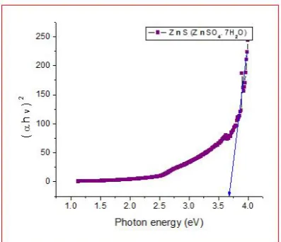
The absorption of ZnS (ZnSO4. 7H2O) is higher as compared
[image:3.595.303.562.82.150.2]to the ZnS. The direct optical band gap of the ZnS is found out from the UV extrapolation graph as shown in Fig.4a and Fig.4b respectively. The ZnS optical band gap is numerically match with previously reported articles (Xiaosheng et al., 2001). Optical band gap is once again confirmed the ZnS as a deposited element. The other optical parameters are calculated from the UV data, which are tabulated in Table 1.
Fig. 4a. Typical UV Energy spectrum obtained for ZnS (ZnSO4. 7H2O) single layer under deposited condition
Fig. 4b. Typical UV Energy spectrum obtained for ZnS (Zn (CH3COO)2.2H2O) single layer under deposited condition
Thermal Conductivity of ZnS buffer layer of thin films
The conduction of heat in semiconductors has been the subject of intense study in the past few years. The thermal conductivity is one of the basic characteristics of semiconductor materials. Thermal conductivity is an important parameter in determining the maximum power under which a semiconductor device may be operated. It also determines the efficiency of the semiconductors used in thermoelectric energy conversion (Rong et al., 2009). The thermal conductivity of semiconductor is a great importance for the performance of thermoelectric coolers and power convertors as well as optoelectronic devices. Low thermal conductivity materials are desired for thermoelectric elements in order to reduce the back flow of heat from the hot to cold junction, while high conductivity materials are necessary for optoelectronic devices in order to dissipate heat (Prema Rani and Saravanan, 2011). Whenever there is thermal gradient in matter, heat transport takes place tending to annul the gradient. This transport of heat energy is described in terms of the coefficient of thermal conductivity K defined as,
Q = - KA (dT/dx) (1)
Where Q is the heat energy flowing in one second across a plane of area A across which there is a thermal gradient (dT/dx). For transport of heat, carriers are necessary; in gases and liquids, the molecules themselves are the carriers. In solids, the carriers are phonons in insulators and electrons as well as phonons in metals. A simple treatment based on the kinetic theory gives the following relation for K,
K = (1/3) Cvυλ (2)
Where Cvis the specific heatat constant volume, υ and λ the
mean velocity and mean free path of the carrier respectively. Thus any scattering event involving phonons and, say, an
impurity, that limits λ contributes to K. the temperature
variation of the thermal conductivity of crystals in different ranges can be explained in terms of the temperature variation of the three quantities in Equation (2)
[image:3.595.65.264.370.537.2]The thermal conduction in solids is intimately linked with the anharmonicity of thermal vibrations. Thus, if thermal vibrations were harmonic, the thermal conductivity would be infinitely large. A number of factors like impurities, dislocation and crystal boundaries contribute to thermal conduction in solids. The coefficient of thermal conductivity of a crystal relates the components of thermal energy flow (a vector) to the components of the thermal gradient (also a vector) and is, hence, a second rank tensor. Thus the number of independent coefficients ranges from one for the cubic class to six for the triclinic class. Before the actual experiment, the
Table 1. Values of optical parameters evaluated from the UV spectrum of ZnS thin film prepared by CBD
Sample name Extinction
Efficient (k)
Refractive Index (n)
Thickness of the film(t) nm
Energy
gap(Eg)eV
ZnS (ZnSO4.
7H2O)
564.864 x 10⁻⁷ 2.41 44 3.66
ZnS
(Zn(CH3COO)
2.2H2O)
[image:3.595.64.263.573.744.2]Table 2. Conductivity of the ZnS thin film for different chemical analysis
Buffer layer of Thin Film (Fabrication of CIS solar cell (PV))
Steady State Temperature
Thermal Conductivity (Kc)
Glass/ZnS (ZnSO4. 7H2O) 63 0.89650W/K-cm
[image:4.595.42.282.163.225.2]Glass/ZnS (Zn (CH3COO)2.2H2O) 62 0.8746 W/K-cm
Table 3a. Temperatures at A, B, C, D under Steady State Conditions for ZnS (ZnSO4. 7H2O) Thin film
Junction Distance from one end (cm)
Thermo emf x (mv)
Temperature y = 22.966 x + 30.321 (°C)
A 0.3 1.27 59.48
B 2,2 0.88 50.53
C 2.938 0.57 43.41
[image:4.595.41.286.265.534.2]D 4.888 0.66 45.47
Table 3b. Temperatures at A, B, C, D under Steady State Conditions for ZnS (Zn (CH3COO)2.2H2O) Thin film
Junction Distance fromone end (cm) Thermo emfx (mv) Temperature y = 22.966x + 30.321 (°C)
A 0.3 1.24 58.79
B 2,2 0.85 49.84
C 2.938 0.59 43.87
[image:4.595.50.276.554.747.2]D 4.888 0.69 46.17
Fig.5a. Temperature vs. thermo emf ZnS (ZnSO4. 7H2O) thin film
Fig.5b. Temperature vs. thermo emf ZnS (Zn (CH3COO)2.2H2O)
thin film
thermocouple has to be calibrated. The temperatures of the thermocouple junctions can be obtained from the thermo emfs read from the millvoltmeter and using standard data on thermocouples. If, on the other hand, a spot-galvanometer is used, then calibration of thermocouples has to be done by using standard temperatures or, a water-bath and thermometer combination. A blank heating of the brass rod R1 may be
carried out by using the variac to determine the temperatures produced by applying different voltages. It is better to choose the voltage such that the temperature T1is about 80° C. The
rods R1and R2,the heater H and the crystal are properly set
and held in position by gently pressing P and then locking it. The heater is switched on applying proper voltage and the temperatures of four thermocouples read off periodically until two or three successive readings do not show any change indicating steady state conditions. The temperatures are recorded. The crystal thickness and the distances of the thermocouples from the lower end of R1are measured (these
are seen in Table 3). The temperatures are plotted (as seen in Fig.5a and Fig.5b) against the distance and the gradients are calculated. Kc is the coefficient of thermal conductivity for
crystal, is then calculated from Equations (3, 4). This value is as seen in Table 2.
Kc= [Km(dT/dx)m]/(dT/dx)c (3)
(dT/dx)m= (dT1/ dx1)m+ (dT2/dx2)m (4)
Where,
Kc–Thermal conductivity of the crystal.
Km–Thermal conductivity of the metal (Brass).
(dT/dx)m–Temperature gradient of the metal.
(dT/dx)c–Temperature gradient of the crystal and these results
are tabulated
Conclusion
Grain size and inter atomic distance were carried out by using X-ray diffraction pattern on the buffer layer. Optimal thickness of active region depends on the optical absorption, nonradioactive processes, and radioactive losses. Total internal resisting forces are resultants of continuously distributed normal and parallel forces that are of varying magnitude and direction and are acting on elementary areas throughout the material. The result indicates that the conductivity of the buffer layer is generated the carriers with minimal losses while coupling light to the junction with minimum absorption losses, yields a highly efficient solar cell.
REFERENCES
Anuar, K., J.H. Mohd, Y.R. Mohd, W.T. Tan, H.A. Abdul,
S.M. Ho, and N. Saravanan, “Chemical bath deposition of NiSe thin films from aqueous solution,” Kuwait J. Sci. Eng., Vol. 37, pp. 63-73, 2010.
Anuar, K., S.M. Ho, W.T. Tan and C.F. Ngai, “Influence of
triethanolamine (complexing agent) on the chemical bath
deposited NiS thin films,” Am. J. Appl. Sci., Vol. 8, pp.
359-361, 2011.
Asenjo, B., C. Guilln, A.M. Chaparro, E. Saucedo, V. Bermudez, D. Lincot, J. Herrero, and M.T. Gutirrez,
“Properties of In2S3 thin films deposited onto ITO/glass
Ezema, F.I. and R.U. Osuji, “Band gap shift and optical
characterization of chemical bath deposited CdSSe thin
films on annealing,”Chalcogenide Lett., Vol. 4, pp. 69-75,
2007.
Gopakumar, P.S. Anjana, and P.K. Vidyadharan, “Chemical
bath deposition and characterization of CdSe thin films for
optoelectronic applications,” J. Mater. Sci., Vol. 45, pp.
6653-6656, 2010.
Hankare, P.P., P.A. Chate, M.R. Asabe, S.D. Delekar, I.S.
Mulla, and K.M. Garagkar, “Characterization of Cd1 -xZnxSe thin films deposited at low temperature by
chemical route,” J. Mater. Sci. Mater. Electron., Vol. 17,
pp. 1055-1063, 2006.
Kim, M.J., H.T. Kim, J.K. Kang, D.H. Kim, D.H. Lee, S.H.
Lee, and S.H. Sohn, “Effect of the surface roughness on optical properties of CdS thin films,” Mol. Cryst. Liq. Cryst., Vol. 532, pp. 21-28, 2010.
Li, Y.C. Zhang, and M. Zhang, “Preparation of SnS2 thin films by chemical bath deposition,” Mater. Sci. Forum.
Vol. 663-665, pp. 104-107, 2011.
Lokhande, C.D., V.S. Yermune, and S.H. Pawar,
“Electrodepositions of CdS, ZnS and Cd1-xZnxS films,”
Mater. Chem. Phys., Vol. 20, pp. 283-292, 1998.
Oikkonen, M.,T. Tuomi, and M. Luomajarvi, “Density of ZnS
thin films grown by atomic layer epitaxy,”J. Appl. Phys.,
Vol. 63, pp. 1070-1072, 1998.
Oladeji, L. Chow, I.O. “A study of the effects of ammonium salts on chemical bath deposited zinc sulfide thin films” Thin Solid Films Vol. 339, pp148-153, 1999.
Prema Rani, M., R.Saravanan, “Influence of silicon and boron
doping on the thermal conductivity of n-GaAs single
crystals”, Materials Science Forum, Transtech Publications, Vol 671, (2011), pp 153-163.
Rong, Y.Y., Y.X. Hong, C.J. Xian, X. Yang, M.Y. Liang, X. Jun, and Y.H. Lin: Chinese Physics Vol.13 (2009), p.2109. Shao, L.X., K.H. Chang, and H.L. Hwang, “Zinc sulfide thin
films deposited by RF reactive sputtering for photovoltaic
applications,”Appl. Surf. Sci., Vol. 212-213, pp. 305-310,
2003.
Ubale, A U,V S Sangawar and D K Kulkarni, “Size dependent
optical characteristics of chemically deposited
nanostructured ZnS thin films” Bull. Mater. Sci., Vol. 30,
pp. 147–151, 2007.
Xiaosheng Fang, Tianyou Zhai, Ujjal K. Gautam and et. al.,
“ZnS nanostructures: From synthesis to applications” Progress in Materials Science Vol.56 pp.175–287, 2001 Yamaguchi, K., T. Yoshida, D. Lincot, and H. Minoura,
“Mechanistic study of chemical deposition of ZnS thin
films from aqueous solutions containig zinc acetate and thioacetatmide by comparison with homogeneous
precipitateion,” J. Phys. Chem., Vol. 107, pp. 387-397,
2003.
Yano, S., R. Schroeder, B. Ullrichand H. Sakai, “Absorption
and photocurrent properties of thin ZnS films formed by pulsed-laser deposition on quartz,” Thin Solid Films, Vol.
423, pp. 273-276, 2003.