FT-68X ·Single Board Computer Reference Specification
TABLE OF CONTENTS SECTION
1.0 1.1 1.2 1.3 1.4 1.5
1.6
1.7 1.8 1.9 1.10 1.11 1.12 1.13 1.14 1.15 2.0
3.0
TITLE
2
-FT-68X Specification Summary
PAGE
Mu1tibus Interface Characteristics PI Connector
System Master Operation System Slave Operation System Clock Lines
Read/Write Command Lines Transfer Acknowledge Line
Initialize Line Lock
Address Lines Byte High Enable Inhibit Lines Data Lines
Interrupt Request Lines Interrupt Acknowledge Bus Arbitration
Notes on Read/Wri.te Memory Timing Multibus Interface Characteristics
P2 Connector
Jl and J2 Specifications
4.0 ~Functional Block Diagram
5.9 Operating principles
FT-68X SPECIFICATION SUMMARY PHYSICAL:
WIDTH: "
12.99 in. (.39.48 HEIGHT: 6.75 in. (17.15 DEPTH: .45 in. ( 1.14 WEIGHT: 29.9' oz. ( .512
SHIPPING. WEIGHT: 25.9 oz. ( .654
(without manual)
FORM FACTOR: IEEE P-796 ELECTRICAL:
5 V + 5 %, 4.1 A(max) ENVIRONMENTAL:
OPERATING TEMPERATURE: 9 C TO 59 C STORAGE TEMPERATURE: -19 C TO 79 C
cm) cm) in) Kg) kg)
RELATIVE HUMIDITY: 99 % WITHOUT CONDENSATION INTERFACE:
Bus conforms to IEEE P-796
Interrupt Requests: TTL compatible Serial I/O: RS-423 compatible
SYSTEM CLOCK FT-68X
PROCESSOR:
9.8394 Mhz +/- 9.91%
MOTOROLA 68999 or the equivalent
Direct Addressing to 8 Megabytes of Memory Byte, Word and Longword Data
16 individual 32 bit registers
SERIAL COMMUNICATIONS CHARACTERISTICS Asynchronous:
Synchronous: Bit Synchronous:
5 to 8 bits, 1, 1.5, or 2 stop bits 5 to 8 bits, internal or external sync. Automatic sync insertion, CRC-16
generation/checking
4
1.9 Multibus Characteristics - PI Connector
This section details the Mu1tibus PI interface. All
parenth~tical references given in this section refer to specified paragraphs within the proposed IEEE Mu1tibus Standard, IEEE'P796. 1.1 System Master Operation - (ref P796, 2.1.1)
This carq acts as a Mode 2 system master. This means that it is not li~ited in the time it is allowed to control the bus. However it can operate as one of a set of system masters using built-"in Mu1tibus arbitration logic. Seethe section on Bus Arbitration for further information.
1.2 System Slave Operation - (ref P796, 2.1.2)
This card is designed to operate as a system slave, in its DMA
mode of operation. It accepts Memory Write and Memory Read commands. 1.3 System Clock Lines - (ref P796, 2.1.3.1.1)
The signals Bus Clock (BCLK*) and Constant Clock (CCLK*) are driven to the multibus with the 68009 system clock at 19 Mhz. Both can be optionally disconnected s'ince there maybe more than one system master card in the multibus but only one is allowed to drive these signals. For the 19 Mhz 68000 optiorr, both BCLK* and CCLK* are driven at 9.8304 Mhz. '
1.4 Read/Wr~~e Command Lines- (ref P796, 2.1.3.1.3)
The signals MWTC*, MRDC*, rowc*, and IORC* are' generated onboard for write or read access to memory or to memory mapped I/O devices. Varies from definition of P796 in that a 24 ma drive capability is provided instead of the 32 rna specified in P796. 1.5 XACK* - (ref P796, 2.1.3.1.3)
Conforms 'to the multibus definition except that the timeout period is 12 microseconds instead of 1 millisecond. A short timeout guarantees that the 68000 can resume normal operation and satisfy real-time requirement~
6 -1.6 INIT* - (ref P796, 2.1.3.1.4)
This signal is driven to the Mu1tibus from the on-board precision vo1tage,comparator, generated when the supply voltage falls below 4.7SV.' It can be optionally disconnected. INIT can be opti'ona11y driven from the Mu1tibus overriding the on-board RESET. 1.7 LOCK* - (ref P796, 2.1.3.1.5)
This signal is not supported.
1.8 Address Lines - (ref P796, 2.1.3.2.1)
This card drives the 29 least significant of the 24 available Mu1tibus address lines. Can optionally be jumpered for connection to the upper 4 lines.
1.9 BHEN* - (ref P796, 2.1.3.2.2)
This signal is generated on this card for 796 bus accesses.
It is software controlled by use of byte or word instructions. Internally, the system accesses its memory as a sequence of l6-bit words. The
expansion memory sold by Forward Technology for this card does not decode its address or data from the P1 connector and therefore the BHEN* signal is not required for correct access to the expansion memory.
1.19 INH1* and INH2* - (ref P796, 2.1.3.2.2)
These are multibus inhibit lines. These signals are neither generated noi-responded to by this card.
1.11 Data Lines - (ref P796, 2.1.3.3)
1.12 Interrupt Request Lines - (ref P796, 2.1.3.4.1)
Supports a total of 7 levels of interrupt. Interrupt priority conforms to the 68B00 definition which labels the 7 levels as INTI (l'owest priority) through INT7 (highest priority, -non-maskable) interrupt. INT0 is not supported since the 68800 only has 7 levels of interrupt available.
All interrupts are handled by the 68BBB as Auto-vectored interrupts. This means that the card itself is defined as having non bus~vectored interrupts and conforms to the definition given in P796, par. 2.3.2.1. Basically, the system, when it interr'upts, need not (shall 'not) respond with an interrupt vector in that the 68BBB already knows where to go to handle that type of interrupt.
1.13 INTA* - (ref P796, 2.1.3.4.2)
This is the interrupt acknowledge line, only used for systems in which "the bus-vectored interrupt type is used. This signal is not supported by this card. (See 1.12)
1.14 Bus Arbitration - (ref P796, 2.1.3.5)
Bus arbitration is controlled by an onboard Intel 8289 Arbiter. It handles Bus Request (BREQ*), Serial Bus Priority signals (BPRN* and BPRO*) and the bus busy signal (BUSY*). Common bus request (CBRQ*) operation is NOT supported. . Serial Priority as defined in P796, 2.4.2.1, is supported. Parallel Priority, P796, 2.4.2.2, is not supported. In the serial mode, up to three system maste~s" may be coresident in the system, more if the user implements parallel priority logic.
1.15 Notes On Read/Write Memory Timing
The FT-68X is IEEE-P796 compatible as described in the preceeding paragraphs of this section. The P796 bus is an asynchronous bus, accommodating devices with various transfer rates while maintaining maximum throughput. A timeout is provided to abort Multibus 'cycles if the addressed device does not respond within
12 microseconds. Note c
-however that the highest performance is achieved by operating the 68BBB from onboard memory. Accesses to the Multibus stretch:"the 68BBB cycle by an amount proportional to the device access" time. The FT-68X contains 256K bytes of dynamic RAM with byte
- 8
2.9 Multibus Specifications - P2 connector
The P2 connector is not intended to be bussed to anything other than the Extended memory card P2 connector. This connection is accomplished using a pair of 69 pin connectors which are directly wired pin 1 t6 pin 1, pin 2 to pin 2 and so forth for the entire set of 69 interconnects~
There are no power connections within the P2 connector, only signal (address lines, data lines) and ground. Connections are made as' specified in the "P2 Connections· diagram which is pro vided at the back of this document •
.
3.9 Onboard Jack and Jumper Specifications
The following chart details the connections for Jacks Jl and J2. Jack Jl is the serial input/output port (TCOM) connector. Jack J2 is the parallel input port connector.
SIGNAL NAME PIN i
Transmit data (TXD) 5 Receive data (RXD) 3 Signal Ground (GND) "13 Request to Send (RTS) 7 Clear to Sent (CTS) 9 Data Set Ready (DSR) 11 Carrier Detect (DCD) 15 Transmit data (TXD) 28 Receive data (RXD) 39 Signal Ground (GND) 38
walCH INTERFACE
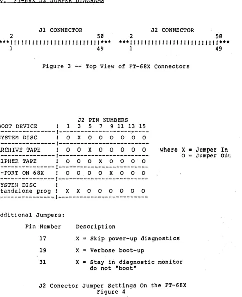
V. FT-68XJ2 JUMPER DIAGRAMS
J1 CONNECTOR J2 CONNECTOR
2 50 2 50
*** 1 1 I ! I ! 1 I I 1 J J I J ! I!! ! J J J J I J *** *** I J J 1 I 111 II! I I I ! ! 1 I I I J J 1 1 1***
1 49 1 49
Figure 3 -- Top View of FT-68X Connecto~s
J2 PIN NUMBERS
BOOT DEVICE 1 3 5 7 9 11 13 15
---!---~----SYSTEM DISC ! 0 X 0 0 0 0 0 0
---1---ARCHIVE TAPE I 0 0 X 0 0 0 0 0
---1---
where Xo
::I = Jumper In Jumper OlitCIPHER TAPE 1 0 0 0 X 0 0 O' 0
---1---B-PORT ON 68X 0 O. 0 0 X 0 0 0
---1---SYSTEM DISC I
standalone prog! X X 0 0 0 0 0 0
---~1---Additional Jumpers:
FT-3~HH~
Pin Number 17
19 31
Description
X
=
Skip power-up diagnostics X = Verbose boot-upX
=
Stay in diagnostic monitor ·do not "boot"J2 Conector Jumper Settings On the FT-68X Figure 4
[image:10.613.48.531.77.669.2]JACK J2:
SIGNAL NAME MEANING J2 PIN t
IN9 Input bit 9 91
IN1· Input bit 1 93
IN2 Input bit 2 95
IN3 Input bit 3 97
IN4 Input bit 4 09
INS Input bit 5 11
IN6 Input bit 6 13
IN7 Input bit 7 15
IN8 Input bit 8 17
IN9 Input bit 9 19
IN19 Input bit 19 21
IN11 Input bit 11 23
IN12 Input bit 12 25
IN13 Input bit 13 27
IN14 Input bit 14 29
IN15 Input bit 15 31
SET INIT* Active contact of INIT toggle 45
REF* Halt indicator output 47
All even numbered pins are grounded. JACK JPl
Pin 1 to 2 jumper: Connects +5V to Jl-19 Pin 3 to 4 jumper: Connects +5V to Jl-33
Note that this . MUST NOT BE USED if the current draw pin is greater than 199 mae
JACK JP2
Pins 2-7, 4-9, 5-6 closed, remainder open configures communications port B for RS-423 or RS-232.
Pins 1-6, 3-8, closed, remainder open configures communications port B for noninverted TTL use. JACK JP3
Pin 1 to 3 jumper: Use for 2716 PROMs
Pin 2 to 4 jumper: Use for 2732, 2764 PROMs
NOTE: Do NOT connect both jumpers, use only ·one or the other.
11 -JACK JP4
These are test points onlyl Use NO jumpers here. Pin Name
1 SYS.ACCESS* 2 +5V
3 CLK29 4 GND
5 TIMEOUT* 6 DTACK* 7 BERR
8 ·GND JACK JP5
Pin 2 to 4 jumper: Drive interrupt 15 with 7291 USART Pin 1 to 3 jumper: Drive interrupt 16 with AM9513 timer 2 JACK JP6 - Bus Control
The following chart details the connections at JP6 which specify the option selection for Multibus co~trol.
Pin 1 to 2 Jumper: Resets 68K from Multibus Pin 3 to 4 Jumper: Drives INIT to Multibus Pin 5 to 6 Jumper: Drives BCLK to Multibus
Pin 7 to 8 Jumper: Grounds BPRN for first Master in the chain.
Pin 9 to 10 Jumper: Drives CCLK to Multibus.
-NOTE: jumpers·I-2 and 3-4 CANNOT BOTH be made. JACK JP7
Pin 1 to 3 jumper: Activate DMA with BA19 Pin 2 to 4 jumper: Activate DMA with BA23
Jack JP8 - Interrupt Control
The following chart det'ails the connections at JP8 which specify the opt~on selection for Multibus Interrupt Response •
..
SIGNAL NAME PIN-TO-PIN
*
MEANINGB.INT7 1 2 (non-maskable interrupt)
B.INT6 3 4 (used by timer 2)
B.INT5 5 6 (used by UART)
B.INT4 7
---
8( *
dotted lines specifyB.INT3 9
---
19 factory installed jumpers)B.INT2 11 12
B. INTI 13 14
B.INT9 15 ---- 16 (not used) JACK JP9
Pins 4-5, 1-2 jumpers: Always on a 68X board
Pins 5-6, 2-3 jumpers: If a 68X substrate is being wired as an extended'memory JACK JPlO
Pin 3-4, 7-8, 11-12: Implements 20 bit multibus addressing. Pin 1-2, 5-6, 9-10 : Implements '24 bit multibus addressing. JACK JPll
13
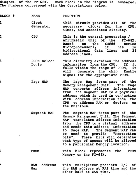
-4.9 Functional Block Diagram
Figure One, bound at the back of this document, shows a block diagram. of the FT-68X. Each block in the diagram is numbered. The numbers correspond with the descriptions below.
BLOCK t
1 2 3 4 5 6 7 NAME Clock Generator CPU
PROM Select Logic
Page MAP
Segment MAP
PROM
RAM Address Mux
FUNCTION
This circuit provides all of the necessary clocks "for the CPU, Timer, and associated circuity. This is the central processing / arithmetic unit of the FT-68X. Based on the 68999 series Microprocessors, it has 16 bidirectional d~ta lines and 24 address lines.
This circuitry examines the address information from the cpu. If it falls within the range of PROM, it will generate the chip Enable Signal for the appropriate PROM. The Page Map forms part of the Memory Management Unit. The Page MAP converts address information from the segment MAP to a physical address which is used in conjuction with address information from the CPU to address RAM or devices on the Multibus.
The segment MAP forms part of the Memory Management Unit. The Segment MAP translates address information from the cpu to a virtual address and sends this address information to Page MAP. The Segment 'MAP can be used· to provide ·p.1,"otection bits". These bits will determine what type of acce~s will be allowed to a particular Memo.ry location. This block represents the
[image:14.612.56.533.124.723.2]8 9 19 11 12 13 14 15 16 17 18 19
RAM Clock Generator Address Bus Drivers RAM
Data
Transceiver Parity RAM
Parity Generator Parity Error Detection
Parallel Input Port
The RAM clocks .(RAS & CAS) are
generated by this circuitry.
These drivers provide address .information to the multibus.
This block represents the RAM Memory of the FT-68X. The standard board has 256k of.RAM.
The data transceiver allows data to flow from/to the RAM Memory.
This portion of RAM is used to store parity information generated by the parity generator.
The parity generation circuit examines the data flowing to/from RAM and generates a parity bit. The parity error detection circuit examines-the output of the Parity generators. If an error is detected this circui.t will notify the CPU. The parallel input port is 16 bits wide.
Bi-Directional These drivers handle all data Bus Drivers communications between the FT-68X
and the Multibus. USAR1'
Transmit Drivers Receive Drivers
The USART converts parallel Data from the CPU to Serial Data to be sent to an external device; i t also converts serial data from an external device to parallel data for use by the cPU. The USART is programmable and is capable of using either .asynchronous or synchronous protocols.
29
21
22
5.9 OPERATION
Timer
Interrupt Logic
DMA
15
-The timer is a programmable device with 5 independent sections. Two of the sections are dedicated to providing the TCOM clocks to the ·USART. One .section is used for Memory Refresh, another Section is utilized as a watchdog timer. The remaining section is for user applications.
The interrupt logic examines interrupts from·the TCOM, Timer, and Multibus circuitry and passes the interrupts on' to the
cpu.
The DMA logic routes addresses to a section of multibus memory into the M68999 local memory.
This section assumes that the user ha~ correctly installed the FT-68X in a Multibus compatible chassis. An ASCII terminal capable of 9699 bits per second operating must be connected to serial port A. It also assumes that the user has installed a RESET switch. The latter item is not essential, but makes the procedure that follows much easier to perfor~, (rather than powering up again).
5.1 Initializing the FT-68X
Ensure that power is applied to the terminal connected to the FT-68Xo Apply power to the Multibus chassis. This also applies power to the FT-68X. On power up, the FT-68X sends a message similar to the following to the terminal:
FTI GATEWAY MONITOR, VERSION 1-49999 BYTES OF MEMORY
If this message does not appear, check the terminal status and the terminal-to-FT-68X connection. If these check out correctly, toggle the RESET switch. The message should appear.
If all the connections and-power are correct and repeated use of the RESET switch fails to generate the message, the FT-68X may be defective.
Successful receipt of the message means that the FT-68X has performed a complete initialization procedure, and that the processor board can be assumed to be operating normally. The
>
17
-- Write the memory refresh routine and initial trap and vector settings into the first 2Kb of RAM. Execution of the·memory refresh routine is started. - Sets the USART channels A & B to 96S9 baud
asynchronous ASCII protocol.
- Initializes and starts the counter/timer functions. - Sets the Supervisor/Stack (SS) pointer to address
X·, 9 917 fe' •
,
- Sets the User Stack (US) pointer to the top of available on-board memory.
- Sets the memory map Segment Table for context 0 and protection level 5 (Supervisor mode has
read, write, and execute access to every segment). - Sets the memory map Page Table. Existing pages of
on-board RAM are mapped so that the physical and virtual addresses are identical.
- Trap vectors are set so that Monitor gains control of any exception interrupt.
Physical address space is divided into eight parts as follows: X, SSS9S' through X 'lFFFFF': Mapped address space'. The standard board has 256 Kb of on-board RAM, but may optionally have
512 Kb. This space can also be mapped to the Multibus I/O or Multibus memory space.
X'2999S9' through X'3FFFFF': On-board PROM 9. are: X'299999' to X'29lFFF' for S Kb
X'299999' to X'293FFF' for l6Kb
Actual addresses
X'49S999' through X'SFFFFF': On-board PROM 1. Actual addresses are: X'4999SS' to X'49lFFF' for S Kb
X'499000' to X'493FFF' for 16 Kb
X'6909ge'. through X'7FFFFF': The on-board dual USART. The Channel A data register is at X'6gegee': the Channel A command register is a X'6eeSe2': the Channel B data register is a X'699S04': and the Channel B command register is at X'699S96'. X'SS0S0S' through X'9FFFFF': The on-board counter/timer. The data register is a X'8SSSSS' and the command register is X'Se9SS2'. X'A99909, through X'BFFFFF': The page Map.
X'Ce990S' through X'DFFFFF'.: The Segment Map.
[image:18.612.84.498.87.467.2]5.2 Using The Monitor Program
The Monitor Program performs four basic functions: initializing the processor on power up or RESET, executing the memory refresh routine \ as described above, . communicating with the user via console functions, and providing Emulator Trap service.
The console functions are routines that communfcate with the user via the dual USART. All input/output is done us'ing, -busy-waits,-and the code runs at·the highest interrupt priority. Therefore, if a user program is interrupted with some
exception, the Monitor will run correctly unless the first
2 Kb of RAM has been damaged. If the user program is undamaged, it can be continued after the interrupt and should be
unaffected by the interruption except for the possible loss of some I/O data.
*W A R N I N G*
There are two rules for dealing with the monitor that ordinarily should not be violated.
1. User programs should not modify the context register. 2. User programs should not write indescriminately into the first two kilobytes of RAM.' It is legal for user programs ,to' change exception vectors in Monitor dedicated RAM. However, no 'Changes are allowed to the level 7 autovectbrs at address X'''''''07C' or_.,·:to the User Interrupt Vectors located 'between addresses X'"''''l''''' and X'''BB3FF', inclusive. IF DATA IN THESE ADDRESSES IS CHANGED, THE MONITOR PROGRAM WILL FAIL. It will;be necessary to RESET the FT-68X, and programs/data resident in RAM
will be destroyed. '
19
-The verb is always one alphabetic character, and may be either upper or lower case. Space* means that any number of spaces between the verb and argument/carriage return are ignored. Argumen~ is normally either a hexadecimal number of a single upper or lower case letter. As indicated by the (), the argument may be optional. If an argument is present, it must be followed immediately by a carriage return (no space allowed) to start command execution. If a command is entered incorrectly, it can be changed or cancelled at any time before the carriage return key is pr,essed. Keying BACKSPACE or DELETE (or RUB) erases one
NOTE: The symbol <CR> will be used throughout this to indicate depressing the carriage return the terminal used to communicate with the program.
manual key on Monitor In the description of command' formats that· follow the word open has special meaning. Anytime a memory location, map register, or CPU register is "opened", the name and contents of that address or register is displayed. If you key <CR>, the contents of the address/register remain the same and the'Monitor program
advances,'~othe next address/register. If you key 9 <CR>, the contents of the address/register are set to zero and the Monitor program advances to the next address/register. If you key new hexadecimal value and <CR>, the new value is entered into the address/register and the Monitor program advances to the next address register. Keying Q <CR> or g <CR> returns the Monitor program to general command level, indicated by the > symbol.
For addresses, -next address/register- means the next byte or word of memory with a starting address larger than the current address. In other words, the command ascends· through memory starting at the address given in the first command entered. ,For registers, -next address/register" means followirtg the s~guence:
6899" data registers DO through D7; 68""": address registers A9 through A6; the Supervisor Stack (SS) pointer; the User Stack
(US) pointer; the Status Register (SR); and the Program Counter
5.2.1 Monitor Commands The Monitor'Commands are: >A n<CR>
>B<CR>
>c [address1<CR>
>D n<CR>
>E [address]<CR>
>G [address]<CR>
>H<CR>
>1 Wmode"<CR>
21
-Opens 68999 address
n(where n is 9 to 6). register Set a breakpoint. The Monitor prompts with the old breakpoint address. The' user enters a new address, if desir~d.
Continue a program starting at the address given. If no address is specified, program execution begins at the current address.
Opens 68999 data register n(where n is 9 to 7).
Opens the work .. at memory location address. An odd· address will be rounded down to the next even address.
Start executing a program at· the address, if given. Otherwise, start 'executing at the current program count~r location.
>L "Host Command"<CR>
>M m<CR>
>0 [address]<CR> >P p<CR>
>R <CR>
>S S-Record<CR>
>X Character <CR>
This command is used to differentiate a host computer command from a Monitor command. The "host command" is sent to .computer via USART Channel B. ·The Host nust send a back slash character () to the FT-6SX in order to reestablish communications with the monitor ,after a file has been downloaded. Any data received by the FT-6SX prior to receiving the backs lash ( ) will be ignored. Opens Segment Map register m.
Opens that byte at memory location address.
Opens Page Map register p.
23
-Examples of the use of Monitor commands follow. The first sets memory address 1234 to OFOO. The second sets the contents of the 68999's data register 3 to 99CF. Underlined portions indicate the en,~ries typed by the user. Non-underlined protions are generated by the Monitor.
>e
091234: 0012'36 :
l234<cr>
23CF? 9F99 <CR> 46CF? Q <CR> )d 3 <CR>
D3: 0009023l? OOCF <CR> D4: 91393495? Q <CR> 5.3 Loading Programs
The FT-6SX is downline loaded using Motorola's ·S· record format, so called because each type of record being with a byte containing the ASCII code for an S (start of Record). An ·S"
record is a fefine format used in transmitting and receiving programs and data. There are ten possible ·S .. record types,six of which are in active use, two which are defined but not· in active use and two which are reserved. They are defined as
follows: .
S0 Header Record Active
Sl 16 bit address Data Record Active S2 24 bit address Data Record Active S3 32 bit address Data Record Not Active
54 Reserved
S5 Transmitted Data Record Count Record Active S6 Reserved
S7 32 bit address End of File/Execution Not Active address record
sa 24 bit address End of File/Execution Active address record
S9 16 bit address End of File/Execution Active address record
The "S" record format is shown below:
start record byte address data (as define Checksum
record type count by byte count) byte
S 2 N N XXXXXX yyyy •••••••• yyyy
zz
---
25
-The FT-68X Monitor currently supports only record types 2 and 8 (S2 & S8).
Example"l
S 2
Start
record Record type Checksum=08
00 00 00 06 53 2D 53
08 Byte count
Ell's compliment of El = IE
Example 2
S
Start record
8
Record type
04 Byte count
Address
00 00 00
Execution address
"6532D53 Data
FB Checksum byte
IE
Checksum byte
The maximum ·S" record length is 79 frames (a frame is defined as one-byte).
Checksum = 04
00
00
"0
When using the S8 record type, an execution address of 999990 will cause no execution to occurl all other addresses are valid. A typiqal file to be transmitted would be made up of the followiri9 sequence:
(LEADER) nx (S RECORD) (TRAILER)
The leader is a string of a minimum of 32 nulls followed by a carriage ~eturn, line feed, and null, sequence. The trailer is a string of a.minimum of 32 nulls.
A tra'iler must appear and goes at the end. Each S record is
loaded into memory, starting with the address specified in the S 2 record, provided it passes the checksum test. The trailer serves two functions: to terminate reading theS-records and. to load the program counter with the starting address. This is the mechanism for defining the entry point ofa program. Program execution can then be started by issuing the G coinmand~
5.4 DMA
The DMA circuit functions to translate the top, half of the mlllti-bus address space through the 68K mapping hardware into the local memory.
In the 29 bit multibus mode, (see jumpers JP7 and JPl0) , any multibus memory command from 9x89099-9xFFFFFwill' be translated
through the 68K segment and page maps into 68X local memory. In the 24 bit multibus mode, (see jumpersJP7 and JP19) , any
multibus mem<?~y command from 9x800909-9xFFFFFF will be translated through the 68X seg~ent and page maps into 68K local memory.
Local memory can be from 256K to I Megabyte and is accessed by the 68K over the P2 connector.
Note: The 68K writes to its local memory directly. It does not (and MAY NOT) attempt to access multibus memory space to DMA into its own local memory. Only peripheral controllers to the 68X use this DMA.
The DMA is used as follows:
Software sets up the 68X context register"F" segments 48 (decimal) and above to map the upper half
(9x89999-BxFFFFF) of the multibus memory (or some part thereof) to 68X local memory.
Note two items here:
- 27
-registers regardless of which context the 68X is executing.
Second, DMA occurs in segment (decimal) 48 to 64
At this point, when any controller attempts a multibus access to the upper half of multibus memory, it will be routed into 68X local memory. Note that you may not have
mU~,~ibus memory (hardware) in this space in that a conflict between the two devices will occur, accessing multiple
devices at the same address.
Thus, in a 29 bit multibus mode,.you may have 1 megabyte of local memory and 1/2 megabyte of non-DMA multibus memory.
In·~a 24 bit multibus mode, you may have 1/4 ~egabyte of local memory and 8 megabytes of non-DMA multibus memory.
6.9 INSTALLATION
The FT-68X board physically conforms to the standards set by the IEEE P-796 form factor. Consequently, the easiest method of installing a FT-68X board in a system is to construct the '. system using a Multibus standard chassis. Such chassis are commercially available from several sources. In addition, the IEEE P-796 standard provides sufficient information for the user to design .a chassis to meet the specific application requirements.
If the user is integrating the FT-6SX into an already existing chassis that does not conform to IEEE P-796 standards, the responsibility for .. insuring rigid mounting with proper clearance from other boards in the' system is the user·' s. . As a·minimum, however, the board should be mounted on 9.6 inch centers parallel to other large boards. An adequate supply of dooling air, either convection or forced, 'is essential. The"" FT-68X consumes approximately 16 watts of power when running. ·Befo~e performing the installation procedure described below, be sUre to remove power from the system.
Inspect the board. If any components are mounted in sockets, ensure that they are firmly seated in their sockets (EPROMS' at U191 and U193, and possibly U195).
Insert the FT-68X PI connector into the 86 pin Multibus connector (Viking 3 KH 43/9Am2 or equivalent). This connect or should be wired for DMA device use -- that is, BPRN is forced low unless there is a multimaster environment.
__ .. __ .Il .. _ .. ~1:Ht ... m~ID9r;y E!xp_al1~i_Qn boar~ (MEB), is being u.sed, .1nstal1it in
- 29
A female 59 pin leader connector (Augat .part number 119-59991-1-2 or equivalent) is required for access to the Serial I/O ports on connector J1. Port A and Port B are factory configured for EIA-RS423 level signals, using a 9699 baud asynchronous data rate.
To hook up a terminal via an RS-232c line, make connections as illustrated below. View the FT-68X board from the frQnt, with the bus edge connector down. Viewed this way, JI is the left-most 58-pin connector along the top of the board, and pin I is
the left~most pin in the near row. Even numbered pins are in the far row.'
Don't forget that many terminals require jumpers for: Request to Send - Clear to Send (4 to 5)
Data Terminal Ready - Carrier Detect (29 to 8)
In order to operate correctly, the Ft-6SX receives and transmits at 9699 bits per second.
A switch to reset the FT-6SX can be wired onto 'another 59-pin, connector as shown below. Connect pin 45 th~ough the switch to ground.
The pin numbering of J2 is the same ·as Jl described above, and all of the even-pins are grounded on J2.
momentary contact switch
~-.---:<.r2-45
31 -DEFAULT JUMPERING
The FT-68X comes with the 8289 bus arbitrator installed and jumpered to be the highest priority bus master.. The bus signal BPRN is 'jumpered to ground on JP6 (7 to 8). Also the FT-68X is strapped atJP6 to drive the bus INIT line. If it is desired to use the bus INIT to reset the FT-68X, then cut.JP6 (3 to 4) and put a jumper on JP6 (1 to 2). The FT-6SX supplies an 8 MHz or 9.83 MHz to both BCLK and CCLK via JP6 (5 to 6) and (9 to
Ie).
The dynamic memory refresh method of the FT-68X causes interrupt , to occur every two milliseconds and therefore·interrupt·, is disconnected from the bus by cutting JP8 (1 and 2).
When the Ft-68X is correctly hooked up and jumpered it will respond to power applicaiton with this message:
"FTI Gateway Monitor Version 1.2 -- 49999 bytes of memory"
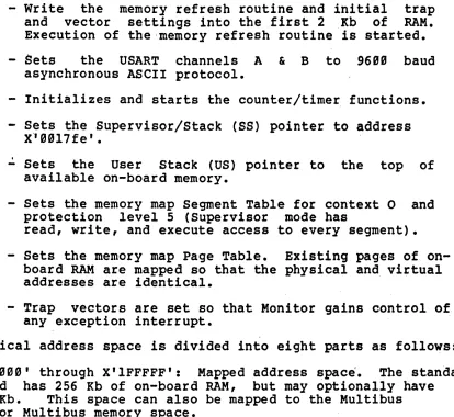
The FT-68X supports RS-423 specifications for voltage driving at +5V.This will support and interface to existing RS-232C hardware. The rise and fall time (slew rate) of .the FT-68X meets RS-232C specifications. To modify the slew rate for longer cables (e.g: 190'-4800'); the RS-423 slew rate of 10-90' must be maintained. To adjust the slew rate for Channel A (TxDa, RTSa and DTRA). Capacitors need to be added at the following locations (refer to the figure below) .•
The capacitor value is dependent on the cable length and modulation rate. Refer to Figure 4.2 for information.
A capacitor of SOpf will increase the rise time' (slew rate) by 3us. The present rise time is lOOns'. A tYP.ical value for' RS-423 specification is 3us, which will support, either a cable length of 100 ft or modulation rate of lOOk bps. If cable length is 58 ft or less, no modification 'should b. done. Ifchannel~A
Multibus P2 Connections
Sig: Name Pin t Sig: Name Pin
,
M.CAS2/---1 M.CAS3/----,---2
M.RASL/---3 M.REF/
---4
M.WE/ ---5 GND
-:---6
M.DIO
---7
M.DII---8
'M.DOO
---9
M.DOI---1"
M.A"---11
GND ---~---12M.DI2
---13
M.DI3---14
M.DS2 ---15 M.D03
---16
M.AI
---17
GND---18
M.DI4
---19
M.DI5---29
M.D04
---21
M.D05 .---22
M.A2
---23
GND---24
M.DI6 ---~--~--25 M.DI7
---26
M.De6
---27
M.D07---28
M.A3
---29
GND --~---3S M.DIL---31
M.DIU---32
M.OOL ---33 M.DCU :<~---"--34
M.A4
---35
GND ~--,----.. ~ 3 6 M.DI8---37
M.DI9 ---~--38M.D08 ---39 M.D09
---4"
M.A5---41
GND---42
M.DI10 ---43 M.Dl11 '--~.---4 4 M.DOle ---45 M.DOII
---46
M.A6
---47
GND, ---~--.. --48M.DI12
---49
M.DII3---59
M.DOI2
---51
M.DOI3---52
M.A7
---53
GND ----~----S4 M.DII4 ---55 M.DIIS---56
M.D014 ----:---57 M.D015
---58
C
680001CPU
~ 00- DATA eus 00-Ol~
eLK 015 GlN ~ eLK
---'--..
AI-A23 PARtly
r l IN1 2 ERROR
[)(TECTJON
AOORESS ~us
. ~ MN I •
'PROM~ j
~
PROM 00
"7' SEltCT ~ C£
lOGIC 3
E-,
RAM
.-OuRCSS MULTI
...MUS PARI TV .~ PARITY !l-DtR[C'T· o A.T "
!tAM GE~. f-I lCWAL . i
12 -tJ 13 DRiVER
-, ,
----
1&FA", [
MAP 7 ~
5((.,,(",
1--I\IN
4 f.1AP RAM D"TA I" 6IT
5
.-
~UM~ TRANS- PARALLEL
, C£lVER
--:-'1 CLot~ CAS ~
, . INPUT
CiENtRATO~ ~ PORT
8 Ie
..
IS
-~ ADORESS BUi DM~
..
MULTIBU$ "DDRESSDRIVER' \.06'C
, MULT\8U$
...
.,
22 eoHT'RO~D'1f OAlA ttOA ~1T' OfU\I£;\S nOA ... JI 11~ER
. .: CLK TXDS 1108
.. IP , JI
f - -
--
1)fT~~t> Itt. -.
---
~DA20 U$ARl . , :' ... JI
I , ' •
flXO & AAO& ~.JI
17
INT. .,
-LOGIC ~
i...-- ~
( MULTleus
1NT ?I
~IG. I
lOOK
t-. LLJ uJ LL:r:
t-t!)·z
W ..J W -l dl c{ 0 10K .-.'- - - . I . . , i~--lK
100 _ .. 10 IK" _ ' W , •
.
i I ... --.--_.-.
;-
"'~-'--., . __ . ... - .... -....,
-
..;
I I
,I."
.
~ ...-_ .... "-t·~ .. ·
i /
~.~ i
V
" ---;..+
.... --..
7
,
t~
,
... r..,V
.
,
V
/
.~.1I
"
.../
~..
V
,
7
,~V
V
.. _- -..
-300
100
RISETIME
}J.SFIG,. 4.2
1M
/
300KV
V
V
~
lOOK 10K·
• ( ....
~ ·f'
~~ ~'~
~.,
( ( ..IK #
(
, ~
c
"
,
(400
, .
100