Electronic Structure Control of Sub-nanometer
1D SnTe
via
Nanostructuring within
Single-Walled Carbon Nanotubes
Andrij Vasylenko,
*
,†Samuel Marks,
†Jamie M. Wynn,
‡Paulo V. C. Medeiros,
‡Quentin M. Ramasse,
§Andrew J. Morris,
⊥Jeremy Sloan,
*
,†and David Quigley
*
,††Department of Physics, University of Warwick, Coventry, CV4 7AL, United Kingdom
‡Cavendish Laboratory, University of Cambridge, Cambridge, CB3 0HE, United Kingdom
§SuperSTEM Laboratory, SciTech Daresbury Campus, Daresbury, WA44AD, United Kingdom
⊥School of Metallurgy and Materials, University of Birmingham, Birmingham, B15 2TT, United Kingdom
*
S Supporting InformationABSTRACT: Nanostructuring, e.g., reduction of dimen-sionality in materials, offers a viable route toward regulation of materials electronic and hence functional properties. Here, we present the extreme case of nanostructuring, exploiting the capillarity of single-walled carbon nanotubes (SWCNTs) for the synthesis of the smallest possible SnTe nanowires with cross sections as thin as a single atom column. We demonstrate that by choosing the appropriate diameter of a template SWCNT, we can manipulate the structure of the quasi-one-dimensional (1D) SnTe to design electronic behavior. From first principles, we predict the structural re-formations that SnTe undergoes in varying
encapsulations and confront the prediction with TEM imagery. To further illustrate the control of physical properties by nanostructuring, we study the evolution of transport properties in a homologous series of models of synthesized and isolated SnTe nanowires varying only in morphology and atomic layer thickness. This extreme scaling is predicted to significantly enhance thermoelectric performance of SnTe, offering a prospect for further experimental studies and future applications.
KEYWORDS: nanostructuring, nanowires, encapsulation, carbon nanotubes, crystal structure prediction, transport, thermoelectrics
F
abrication of low-dimensional nanostructured materialshas attracted much attention because of the extraordi-nary electrical and thermal properties the materials achieve at the nanoscale as well as their versatile applications in nanotechnology. Controllable synthesis of nanowires and fundamental investigation of their properties are essential for
prospective applications including energy conversion1 and
nanoelectronics.2 Regulation of the local structure at the
nanoscale is of particular interest, as it enables the design of the
properties and enhancement of the materials’performance for
specific applications. In particular, optimization of
thermo-electric efficiency can be achieved due to band structure
engineering and reduction of lattice thermal conductivity or
scattering engineering.3−12 Scaling to the lower dimensions
leads to synergy of these strategies for enhancement of
thermoelectric performance;13−15 however, up until recently
this remained practically unachievable for many of the most
promising candidate materials.1 Hence development of
techniques for controlled fabrication of nanowires with a
potential to regulate local structure is necessary for
improve-ment of the current level of thermoelectric efficiency.
A candidate material, tin telluride, has a moderate
thermo-electric efficiency due to characteristic high thermal
con-ductivity and subsequently low thermoelectricfigure of merit
(ZT) in its pure bulk crystalline form.16−18 However, the
accessible bond hybridization and phase change properties of
SnTe19,20imply rich diversity in local structure,16−18possibly
leading to dramatically different structures under extreme
confinement.21−23Single-walled carbon nanotubes (SWCNTs)
with diameters ranging from 7 to 14 Å can be used as templates
with a controllable degree of confinement for the growth of
quasi-one-dimensional (1D) nanocrystals.21,22,24−27Templating
or encapsulating materials inside SWCNTs as a function of
Received: March 26, 2018
Accepted: May 21, 2018
Published: May 21, 2018
Article
www.acsnano.org Cite This:ACS Nano2018, 12, 6023−6031
copying and redistribution of the article or any adaptations for non-commercial purposes.
Downloaded via 137.205.202.51 on January 31, 2019 at 11:09:41 (UTC).
their van der Waals internal surface has been suggested as far
back as 1997, when Nikolaevet al.28indicated that C60was just
the right diameter to fit in 1.4 nm SWCNTs, subsequently
realized by Smithet al.29We and many others have investigated
the“integral atomic layer”growth of metal halides in SWCNTs
in terms of their van der Waals confinement,30,31 and many
other studies since have explored the confinement and
transport of many other species including, for example,
ions,32 graphene ribbons,33 and, in the narrowest nanotubes,
single atomic chains of silicon.34Senga et al.26 described the
subsequent formation of CsI in DWCNTs, and we recently reported Te atomic chains and coils in the narrowest
SWCNTs;24much of this work has been done with a view to
either tailoring the physical properties of the confining
materials or modifying the properties of the included materials
by confinement. Due to the often unexpected 1D structures
that phase change materials may manifest in extreme
confinement, one cannot deduce their crystallography on the
basis of their known bulk counterparts.24Reduced
dimension-ality, in particular, gives rise to surface effects in electronic
transport and multiple phonon-drag enhancement of
thermo-electric properties.1,15,35,36Understanding the effect of confi
ne-ment on the structure and transport properties can thus enable development of a powerful tool for the regulation of thermoelectric performance in such materials.
RESULTS AND DISCUSSION
Here we study a controlled synthesis of the smallest possible 1D crystalline SnTe nanowires within SWCNTs and the change in their structure and electronic behavior as a function
of varying degrees of confinement. To predict the structure and
stoichiometry of SnTe nanowires encapsulated in SWCNTs, we
employ ab initio random structure searching (AIRSS)37
analyzed via a convex hull construction.38,39 This allows for
visualization of formation energy for a range of available structures and stoichiometries. We then calculate energy of formation from gaseous Sn and Te and determine the thermodynamic stability of SnTe nanowire structures within
SWCNTs of different diameters. During synthesis, we apply a
sublimation technique for the growth of SnTe within
SWCNTs.26 We then employ aberration-corrected high
resolution transmission electron microscopy (HRTEM), aberration-corrected scanning transmission electron micros-copy (STEM), and electron energy loss spectrosmicros-copy (EELS) to experimentally verify the structures obtained, hence demonstrating we have proposed a viable synthesis route.
To study the encapsulated SnTe nanocrystals, we first
identify the most stable structures adopted by this material
when confined within SWCNTs. We previously adapted AIRSS
for the prediction of 1D structures that manifest within
SWCNTs of various diameters.24 In the present work by
applying the same strategy, i.e., by optimizing geometries of
random structures in confinement of explicit CNTs or
confining potential, we generate more than 3100 structures
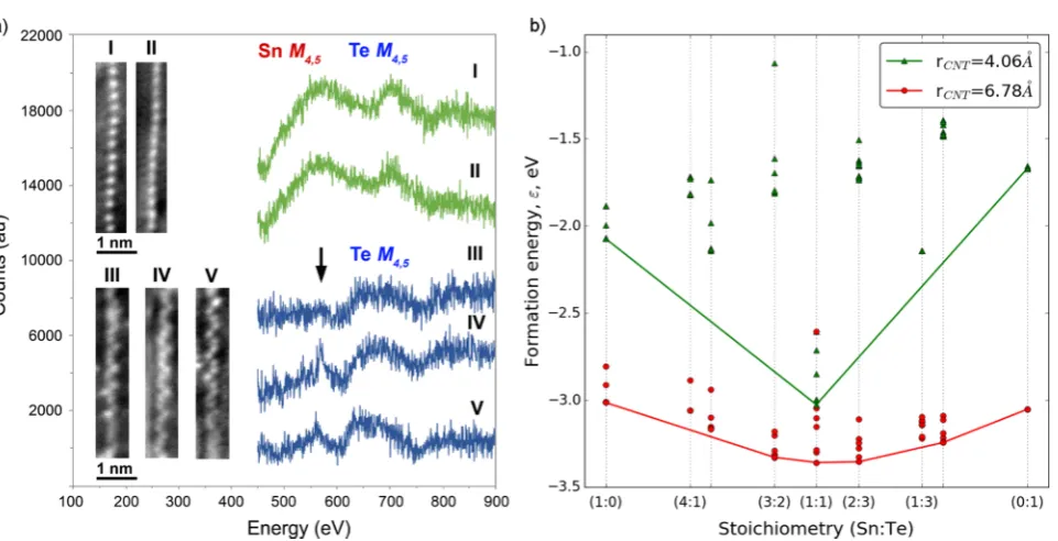
Figure 1. (a) EELS at the outmost electron shells (M-edge) in SnTe 1D atomic chains and Te coils encapsulated within SWCNTs. Note that Te coils are only obtained in nanowires depleted in Sn,24as indicated with an arrow. The small difference in atomic number for Sn (Z = 50) and Te (Z = 52) results in highly similar contrast for these atoms in the observed SnTe experimental images and simulations. However, the summed EELS spectra from images I and II (i.e., obtained from the samefield of view in both instance) show a clear difference in both composition and linear (or zigzag) morphology than from the images and summed EELS spectra from images III to V, the latter showing a coil-like morphology only, consistent with the results we reported for pure Te“coils”in ref 24. (b) Convex hull construction for SnTe nanowires with different stoichiometries embedded in CNT(6,6),r= 4.06 Å and CNT(10,10),r= 6.78 Å. The formation energy per atom is plotted for chemical potentials of Sn and Te relevant to an ideal gas 1:1 mixture with a density of 5.00 g/L at 300 K. In CNTs with small radius (green line) only pure Sn, pure Te, or Sn1Te1nanowires can be formed, with SnTe being the most energetically favorable composition
for infinitely long nanowires. In CNTs with larger diameters (red line) composition selectivity is weaker, such that in small regions disproportionation into 2:3 and 3:2 stoichiometry is energetically competitive. Triangles and circles represent 100 of the lowest formation energies of the structures predicted with AIRSS.
[image:2.625.76.557.61.307.2]with different stoichiometries, encapsulated within a variety of
radii of CNTs. In order to exclude artificial strain in modeling
of the systems with incommensurate sublattices, for calculations of lattice and energy corrections we exploit a theoretical construct of an implicit nanotube: a cylindrical electrostatic
potential that provides steric confinement of SnTe. The
technicalities and justification of such an approach are detailed
in ref24. Sampling of the stoichiometries is important due to
potential disproportionation of the Sn:Te ratio during sublimation of the solid. In the convex hull construction,
formation energyεof the randomly generated structures upon
ab initio optimization of their geometries is plotted against stoichiometry. In this case per-atom formation energy is calculated with respect to the chemical potentials in a reservoir
of ideal gas of Sn and Te atoms, i.e., which are produced via
sublimation of SnTe under typical experimental conditions.
ε= E −E − μ − μ −μ
N X ( )
total CNT
Sn Te Te Sn (1)
where Etotal is the total energy of a nanowire encapsulated
within SWCNTs, ECNT is the energy of the corresponding
pristine SWCNTs, N is the number of atoms in the
encapsulated structure, μ stands for the chemical potential of
the corresponding species, andXTe=NTe/N is the fraction of
Te atoms within the encapsulated structure. Thermodynami-cally stable structures for a given stoichiometry form the convex hull of points, with the lowest energy vertex identifying the
most energetically favorable composition for an infinitely long
nanowire (Figure 1b). These diagrams reveal a selectivity for nanowires with equal proportion of Sn:Te within the smallest
SWCNTs (i.e., green lines in Figure 1b). This finding is
indirectly confirmed by the experimentally obtained EELS that
features peaks from Sn and Te atoms with equal intensity for the single-atom chains formed within the smallest SWCNTs
((I) and (II) inFigure 1a). In SWCNTs with larger diameters
(red lines inFigure 1b), the difference between the formation
energy of the encapsulated nanowires decreases, and compounds with varying stoichiometry other than a 1:1 ratio
become more competitive. Thus, somefinite size regions of the
synthesized samples within larger diameter SWCNTs are expected to be depleted of, or enriched in, Sn. In our
experimentalfindings, we are able to identify a region of the
sample where SnTe with a 1:1 stoichiometry is present within
the same nanotube as helical Te24(see (III)−(V) inFigure 1a).
This unexpected behavior suggests that the kinetics of filling
SWCNTs from the gas phase may lead to inhomogeneities in the encapsulated structures, leading to formation of junctions
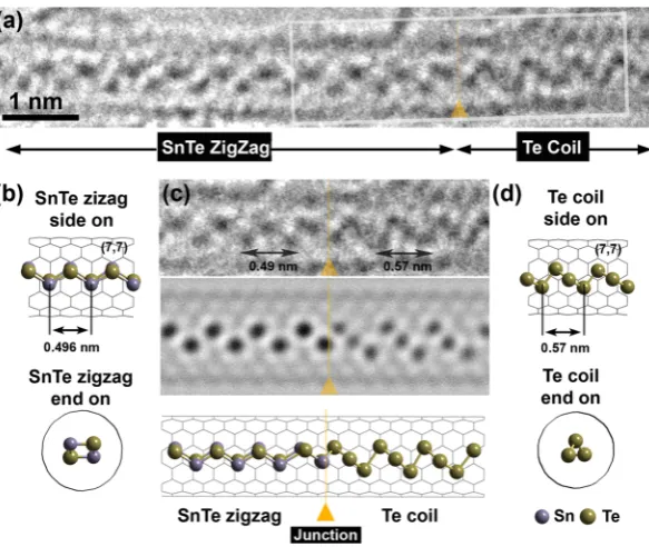
between SnTe and Te nanowires (see Figure 2). These two
nanowire structures as predicted via AIRSS have two
distinctively different motifs and lattice parameters,
commen-surate with those in the HRTEM image. Moreover, geometry
optimization using first-principles indicates that a repeating
periodic realization of this junction occupies a local minimum on the potential energy landscape. A model in which SnTe is forced to form a corresponding helical chain demonstrates dynamical instability and undergoes reconstruction into a double-zigzag structure during minimization of forces. The majority of encapsulated SnTe nanowires exhibit 1:1 stoichiometry at this CNT diameter.
After identifying the lowest energy nanowire structures via
our AIRSS searches, we proceed to studying their relative
stability as a function of degree of confinement within CNTs.
By comparing the formation energy of the predicted structures
within different diameters of SWCNTs, we have established a
strong dependence of the structure formed on the diameter of
the encapsulating SWCNTs.Viaa series of detailed calculations
(see Supporting Information (SI) for the details of methods and calculations) we are able to plot the formation energy of
each nanowire as a function of the confining SWCNT diameter
[image:3.625.166.458.66.312.2]and, hence, identify diameters at which particular structures are
Figure 2. A∼8 nm section of a 0.95 nm diameter SWNT containing two distinct crystalline regions: a SnTe double zigzag and a Te coil region depleted in Sn (cf.Figure 1(a),Figure 4, and ref1). (b) Schematic side-on and end-on views of double zigzag SnTe in a (7,7) SWCNT. (c) Detail from (a), multislice TEM simulation, and structure model of the SnTe zigzag: Te coil junction. (d) Schematic side- and end-on views of a Te coil in a (7,7) SWCNT (cf. ref1).
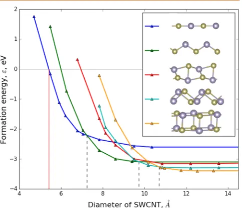
unambiguously stable. The results are shown inFigure 3. The formation energies of all of the investigated structures
demonstrate the same trend as the diameters of the
encapsulating SWCNT increases: first a rapid drop followed
by a leveling offat the value corresponding to noninteracting
nanowire−SWCNTs. We alsofind a lower limit of 5.6 Å for the
smallest diameters of the encapsulating SWCNTs that can be
filled with sublimed SnTe (vertical red line in Figure 3). In
SWCNTs of certain larger diameters (black dashed lines in Figure 3) formation of different structures becomes energeti-cally competitive, and hence transitions may occur between competing nanowire structures. The evolution of the
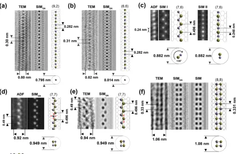
nanostructure adopted by SnTe within SWCNTs with different
diameters is presented in Figure 4, where we compare the
structures predicted by AIRSS to those experimentally
synthesizedviasimulated HRTEM images. We investigate the
mechanical stability of each encapsulated nanowire structure in
a series of ab initio calculations of their lattice vibrational
characteristics (see theSIfor the details of phonon dispersions
in the SnTe nanowires). From the latter, we find that in
confinement in the regions between the transition points (black
dashed lines in Figure 3), the corresponding lowest energy
structures are mechanically stable. A polar linear chain of SnTe while being the most stable structure in the small-diameter CNTs undergoes reconstruction into a zigzag nanowire upon isolation from the CNTs. Phonon dispersions in the isolated zigzag, double-zigzag, and rocksalt-like nanowires retain the stability features, hence indicating the possibility for their isolation from CNTs. The role of encapsulating SWCNTs in
stabilization and electronic interaction with thefilling is further
studied with Bader charge analysis, which does not demonstrate
any substantial charge transfer (see the SI for the details of
Bader charge analysis in the SnTe@SWCNTs compound systems). With chemical interaction between CNTs and encapsulated nanowires being negligibly small, the main interaction between the subsystems in this compound material
isviasteric confinement. We thus conclude that an appropriate
choice of the host SWCNTs can allow controlled structuring of nanowires with increasing coordination numbers, from 1D atomic chains toward bulk-like rocksalt nanowires. Further extraction of the synthesized nanowires is possible due to the
techniques for unravelling SWCNTs.42,43 Alternatively, the
technique for synthesis of nanowires within CNTs performed in this work can be applied to carbon nanoscrolls of appropriate
diameter with their subsequent unrolling.44,45
Electronic band structure engineering, in particular opening of the band gap and convergence of conduction bands, has been demonstrated as a valid route toward improvement of
thermoelectric properties.7,8,12,18Both approaches lead toward
significant enhancement of the Seebeck coefficient and electron
transport in nanostructured materials. We investigate regulation
of the electronic structure in SnTe nanowires via synthesis
within different diameter SWCNTs. We perform a series of
calculations of the k-resolved PDOS and evaluate the partial
distribution of electrons (via Lowdin charge distribution)
during structural evolution of the nanowires (i.e., following the
evolution of nanowire structure and electronic structure in
concert with the indicated arrows inFigure 5). With an increase
in the diameter of confinement, the atomic bond lengths and
angles change, triggering rehybridization of the atomic orbitals and redistribution of the charge on them. On the outermost 5d-orbitals of both Sn and Te, there is a growth of the number of electrons participating in transport. Combined with the increase in the total number of electrons in the larger nanowires as well as the increased number of conduction bands in the vicinity of the Fermi level, the convolution of these factors results in a boost in electronic transport in a rocksalt-like nanowire (see Figure 5a). From first principles, we calculate the electronic
band structure and corresponding effective electron mass
=
*ν ℏ
ν
m
E k
1 1 d d 2
2
2 in the model lowest energy nanowires that can
be synthesized within different diameter SWCNTs. Our
calculations indicate that as the diameter of the confining
SWCNT increases, the electronic band gap of the
correspond-ing nanowire widens and the effective mass of carriers also
increases; hence all of the studied nanowires except for the 1D
linear chain exhibit semiconducting characteristics (seeFigure
6).
Moreover, for the rocksalt-like nanowire that can be formed due to encapsulation inside SWCNTs with diameters >11.2 Å, there is conduction and valence band convergence at the high symmetry points close to the Fermi level, leading to strongly
enhanced transport properties (see Figure 5). The Fermi
surface in all of the nanowires does not exhibit topological anisotropy due to the extreme scale. To demonstrate the
profound effect that a proposed method of engineering of
electronic band structures might have on the functional
properties, we further conduct a series ofab initiocalculations
of electron−phonon τ ∼ ∑ |⟨ |∂ | + ⟩|
∂
ν
−
k Ek q
k q k
1
,
2 el ph
2
2 and
pho-non−phonon scattering τν ∼ ∑ − |∂ ∂∂ ∂− |
−
E
q q q q q q 1
, ,
2 ph ph 0
3
0
and the
ultimate applications, in which SnTe nanowires are isolated from the templates for synthesis, evaluate transport properties by solving the corresponding Boltzmann transport equations
for electrons and phonons. We validate this ab initio-based
[image:4.625.61.303.96.303.2]methodology for evaluation of transport characteristics by calculating ZT for bulk SnTe crystal, for which our results are in close agreement in functional trend and minimum and maximum values with a previous experiment (see red dashed
Figure 3. Evolution of the lowest energy structure as a function of encapsulating SWCNT diameter. Vertical lines indicate the degree of confinement, where formation of SnTe from gas is energetically accessible within a SWCNT (red); structural transitions occur (dashed).
linevsblack circle line in Figure 6). Wefind that the Seebeck
coefficient for the SnTe 1D chain, the double-zigzag SnTe
chain, and the 2 × 2 SnTe rocksalt chain nanowires are all
significantly enhanced in comparison either to the bulk or to
bulk-doped SnTe.40,41 This enhancement coupled with high
electrical conductivity results in an ultrahigh boost of the power
factor, up to 1.9 W/(K2·cm) at 1000 K. Decrease of thermal
conductivity, κ, is another important target that can often be
effectively addressed by reduction in dimensionality.13,35Due to
the surface-dominated phonon scattering, nanowires of small
diameters demonstrate a significant decrease in phonon
lifetimes and thus limited lattice thermal conductivity.13,35
We have previously demonstrated that in nanocomposite
structures SWCNT−nanowire phonon lifetimes can be further
decreased due to the extra pathways for phonon decay.46
Further research is required to investigate how this affects
lattice thermal conductivity of nanocomposite SWCNT−
nanowire, and SnTe in particular. In the case where encapsulation of nanowires induces phonon modes so that more phonons satisfy the selection rules, we can expect
effective redistribution of the phonon population, which may
decrease surface phonon conductivity.47 In such compound
nanostructures, with electronic and thermal transport domi-nated by CNTs, reduction in lattice thermal conductivity would lead to improved thermoelectric performance in comparison to
that of pristine CNTs. This renders nanowires encapsulated in
CNTs as a novel prospect in highly effective thermoelectric
materials.
Here, we show that total thermal conductivity in the smallest isolated SnTe nanowires is dominated by the colossal electron
contribution to heat transport and reaches 9.8 W/(K·m) at
1000 K for the rocksalt-like nanowire (seeSIfor the details of
calculations of transport properties in the SnTe nanowires).
Due to the moderate steepness of the trend, however,κdoes
not exceed 2 W/(K·m) at temperatures below 600 K. As with
the Seebeck coefficient, the resulting overall ZT for SnTe
nanowires that can be synthesized within SWCNTs is
significantly enhanced in comparison to previously realized
figures for bulk doped.41 This is achieved over a wide
temperature range, reaching 3.25 at 380 K for the
rocksalt-like nanowire (seeFigure 6).
CONCLUSIONS
We have demonstrated that the confinement provided by
SWCNTs with diameters from 7 to 11 Å can be exploited as a viable route for synthesis of the smallest possible SnTe 1D nanowires with a tunable electronic behavior. We discovered
several possible, previously unreported, structural confi
[image:5.625.75.553.64.374.2]gura-tions of the atomic scale nanowires that are energetically
Figure 4. Evolution of the SnTe nanowire within SWCNTs of increasing diameters from a single-atom chain (a, b) to a zigzag chain viewed in plan view as indicated by the models and simulations (c) to a double-zigzag chain (d, e) and then a 2×2 rocksalt-like SnTe fragment (f). Some distortions, including asymmetric distortions, are evident in the experimental images in (d), (e), and (f) probably caused by thermolytic interactions between the electron beam and the specimen similar to those reported for SnSe.22To reproduce these effects in the simulations, we have introduced atom column superposition and/or staggering with added“virtual”atoms to reproduce the blur in two directions, as indicated by the small red arrows in the corresponding models on the LHS atoms (d) or the RHS atoms (e) (key: TEM = 80 kV aberration-corrected TEM image; SIMGN= multislice TEM or ADF image simulation with 15% Gaussian noise added; ADF = aberration-corrected
annular dark field STEM image; SIM = multislice ADF image simulation (no noise); SWCNT conformations indicated by integers in parentheses).
preferable within SWCNTs of different diameters. We have determined that electronic structures of the formed nanocryst-als depend directly on the diameters of the encapsulating
SWCNTs used in synthesis, thus offering a practical tool for
band structure engineering and, consequently, high
thermo-electric performance via appropriate choice of templates for
[image:6.625.66.565.56.341.2]synthesis. Exploitation of homogeneous samples of SWNTs with diameters >1.1 nm will enable controlled synthesis of
Figure 5. Electronic population on the outermost p- and d-orbitals of Sn and Te and the partial density of states (PDOS) in encapsulated nanowires within SWCNTs of increasing diameter (in the direction of the arrow). Resolution PDOS in the reciprocal space is represented by the width of the curves. Rehybridization of atomic orbitals during structural evolution results in more electrons reaching 5d-orbitals. Due to the combination of the introduced transformationsincrease of PDOS at the top valence level, more bands crossing the Fermi level (dashed line), and more electrons engaged as carrierstransport properties are enhanced (a).
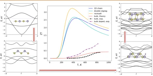
Figure 6. Evolution of electronic band structure, opening of the band gap, and ZT of the corresponding stable SnTe nanowires synthesized in SWCNTs of increasing diameter (in the direction of the arrow). The ZT value for the zigzag structure (green line inFigure 3) does not exceed 0.01 and is omitted for clarity.40Experimental data for ZT of the bulk SnTe are taken from ref18. Experimental data for ZT of the bulk Cd-doped SnCd0.03Te are taken from ref41.
[image:6.625.63.565.404.655.2]rocksalt-like SnTe nanowires with the highest ZT. While the focus of this study was on the smallest 1D nanowires starting from the bottom up, notably a similar trend of increasing
electron band gap and effective mass as inFigure 6 has been
observed with the decrease of the diameter of the nanowires
from∼30 nm.1This indicates the possibility for the existence of
an optimal geometrical parameter (diameter) of the nanowires for which thermoelectric performance may reach its maximum value. With the models of SnTe nanowires isolated upon synthesis in SWCNTs exhibiting unprecedented high
thermo-electric efficiency, previous reports on high ZT of CNTs
themselves48,49 inspire a hypothesis of overall high
thermo-electric performance in a compound material. Verification of
thermoelectric qualities of a compound material is increasingly
possible upon formation of yarns or thin films of SnTe@
SWCNTs and warrants future experimental studies and applications.
METHODS
Sample Preparation.SWeNT SWNTs (0.7−1.1 nm) are supplied in the UK by Sigma-Aldrich but were originally manufactured by
SouthWest NanoTechnologies as a specific grade (i.e., SWeNT SG65i,
Product No. 773735) processed SWNTs produced by the CoMoCAT synthetic protocol. A 30 mg amount of SWeNT CNTs was oxidized in the atmosphere at 750 K for 40 min, reducing to 10 mg. A 70 mg amount of SnTe (Sigma-Aldritch, 99.999%) was loaded into the sealed end of a silica quartz sublimation ampule with the reduced CNTs in the other. The ampule was sealed under argon and heated to 1033 K for 7 days. The SnTe end of the ampule was placed in the center of the furnace, creating a negative temperature gradient toward the CNTs. Approximately 2 mg of SnTe@SWCNTs was dispersed into 20 mL of
2-propanol and sonicated with pulsing (i.e.2 s on / 2 s off) with a
sonic probe for 40 min. Three drops of dispersed CNTs were drop
cast onto a 3.05 mm copper grid with a lacey carbon supportfilm
(Agar Scientific).
Electron Microscopy. The samples were examined in a JEOL double-aberration-corrected ARM200F electron microscope operating
at 80 kV. Data were recorded on a Gatan Orius SC1000 1.024×1024
pixel CCD camera. The STEM-EELS data were acquired on a Nion UltraSTEM100 instrument, operated at 60 kV acceleration voltage and
equipped with a cold field emission gun providing a native beam
energy width of 0.30 eV. The optics were configured to form a 1.1 Å
probe (full-width at half-maximum) of 32 mrad convergence semiangle, with a 40 pA beam current. High- and medium-angle
annular dark-field images were recorded with semiangular ranges of
85−190 and 55−80 mrad, respectively. EELS data were collected with
a Gatan Enfina spectrometer with a collection semiangle of 36 mrad. A
dispersion of 0.5 eV/channel was chosen in order to record
simultaneously the C K SnM4,5 and Te M4,5 edges. This confirmed
that at least 80% of all the observedfilled SWNTs werefilled with
microstructures consistent with our modeling protocols. TEM and image simulations were performed with the SimulaTEM multislice image simulation code using an accelerating voltage of 80 kV, a
coefficient (Cs) of 0.001 mm, and a value of defocus of 7 nm.50ADF
STEM simulations were performed using clTEM, an open source GPU
accelerated multislice program developed by M. A. Dyson.51 The
simulation parameters were matched to the microscope aberrations as measured by the CEOS control software and also duplicating the imaging conditions stated above for either the ARM200F electron microscope operating in STEM mode at 80 kV or the Nion
UltraSTEM100 dedicated STEM operated at 60 kV. Thermal diffuse
scattering was modeled using the frozen phonon method with 15
configurations.
Ab Initio Computations. We employ density-functional theory and density-functional perturbation theory with a plane-wave basis set
as implemented in CASTEP-17.152and Quantum Espresso-6.1.53We
use a wave functions basis set with a cutoffenergy of 400 eV; the
maximum distance in the k-point grid in reciprocal space is 1 Å−1. In
the AIRSS search the total energy is converged within 1×10⁻⁶ eV
tolerance, and the maximum module of forces for geometry optimization is 0.05 eV/Å. Details on employed pseudopotentials,
exchange−correlation functional and convergence parameters for
phonon calculations, band structure, electron−phonon coupling, and
Wannierisation of wave functions are described in the Supporting
Information.
ASSOCIATED CONTENT
*
S Supporting InformationThe Supporting Information is available free of charge on the ACS Publications websiteat DOI:10.1021/acsnano.8b02261.
More information about the structural models, electronic structures, mechanical stability, and charge analysis; details of conducted calculations and exploited methods
for calculation of transport properties52−57(PDF)
AUTHOR INFORMATION
Corresponding Authors
*E-mail: [email protected].
*E-mail: [email protected].
*E-mail: [email protected].
ORCID
Andrij Vasylenko:0000-0002-6933-0628 Paulo V. C. Medeiros:0000-0002-7803-9058 Quentin M. Ramasse:0000-0001-7466-2283 Andrew J. Morris:0000-0001-7453-5698 Notes
The authors declare no competingfinancial interest.
Data used in this work are available via the Warwick data
repository at wrap.warwick.ac.uk/100297.
ACKNOWLEDGMENTS
A.V., P.V.C.M., A.J.M., J.S., and D.Q. thank the UK Engineering and Physical Sciences Research Council (EPSRC) for funding through grant numbers EP/M010643/1 and EP/M011925/1.
J.M.W. acknowledgesfinancial support from the EPSRC Centre
for Doctoral Training in Computational Methods for Materials Science under grant EP/L015552/1. S.M. and J.S. are further indebted to support from EP/I033394/1. The SuperSTEM Laboratory is the U.K. National Facility for Aberration-Corrected STEM, supported by the EPSRC. This work used the ARCHER UK National Supercomputing Service (www. archer.ac.uk).
REFERENCES
(1) Heremans, J. P.; Dresselhaus, M. S.; Bell, L. E.; Morelli, D. T.
When Thermoelectrics Reached the Nanoscale. Nat. Nanotechnol.
2013,8, 471−473.
(2) Ferry, D. K. Nanowires in Nanoelectronics.Science 2008,319,
579−580.
(3) Toberer, E. S.; Zevalkink, A.; Snyder, G. J. Phonon Engineering
Through Crystal Chemistry.J. Mater. Chem.2011,21, 15843−15852.
(4) Zhou, M.; Li, J.-F.; Kita, T. Nanostructured AgPbm SbTem+2
System Bulk Materials with Enhanced Thermoelectric Performance.J.
Am. Chem. Soc.2008,130, 4527−4532.
(5) Biswas, K.; He, J.; Blum, I. D.; Wu, C.-I.; Hogan, T. P.; Seidman, D. N.; Dravid, V. P.; Kanatzidis, M. G. High-Performance Bulk
Thermoelectrics with All-Scale Hierarchical Architectures. Nature
2012,489, 414−418.
Enhancement of Thermoelectric Efficiency in PbTe by Distortion of
the Electronic Density of States.Science2008,321, 554−557.
(7) Pei, Y.; Shi, X.; LaLonde, A.; Wang, H.; Chen, L.; Snyder, G. J. Convergence of Electronic Bands for High Performance Bulk
Thermoelectrics.Nature2011,473, 66−69.
(8) Liu, W.; Tan, X.; Yin, K.; Liu, H.; Tang, X.; Shi, J.; Zhang, Q.; Uher, C. Convergence of Conduction Bands as a Means of Enhancing
Thermoelectric Performance ofn-Type Mg2Si1−xSnxSolid Solutions.
Phys. Rev. Lett.2012,108, 166601.
(9) Zhao, L.-D.; Tan, G.; Hao, S.; He, J.; Pei, Y.; Chi, H.; Wang, H.; Gong, S.; Xu, H.; Dravid, V. P.; Uher, C.; Snyder, G. J.; Wolverton, C.; Kanatzidis, M. G. Ultrahigh Power Factor and Thermoelectric
Performance in Hole-Doped Single-Crystal SnSe.Science 2016,351,
141−144.
(10) Fu, C.; Bai, S.; Liu, Y.; Tang, Y.; Chen, L.; Zhao, X.; Zhu, T. Realizing High Figure of Merit in Heavy-Band P-Type Half-Heusler
Thermoelectric Materials.Nat. Commun.2015,6, 8144.
(11) Shi, X.; Yang, J.; Salvador, J. R.; Chi, M.; Cho, J. Y.; Wang, H.; Bai, S.; Yang, J.; Zhang, W.; Chen, L. Multiple-Filled Skutterudites: High Thermoelectric Figure of Merit Through Separately Optimizing
Electrical and Thermal Transports. J. Am. Chem. Soc. 2011, 133,
7837−7846.
(12) Pei, Y.; Wang, H.; Snyder, G. J. Thermoelectric Materials: Band
Engineering of Thermoelectric Materials.Adv. Mater.2012,24, 6124−
6124.
(13) Wang, Z.; Alaniz, J. E.; Jang, W.; Garay, J. E.; Dames, C. Thermal Conductivity of Nanocrystalline Silicon: Importance of Grain
Size and Frequency-Dependent Mean Free Paths.Nano Lett.2011,11,
2206−2213.
(14) Hochbaum, A. I.; Chen, R.; Delgado, R. D.; Liang, W.; Garnett, E. C.; Najarian, M.; Majumdar, A.; Yang, P. Enhanced Thermoelectric
Performance of Rough Silicon Nanowires.Nature 2008,451, 163−
167.
(15) Hicks, L. D.; Dresselhaus, M. S. Effect of Quantum-Well
Structures on the Thermoelectric Figure of Merit. Phys. Rev. B:
Condens. Matter Mater. Phys.1993,47, 12727−12731.
(16) Tan, G.; Zhao, L.-D.; Shi, F.; Doak, J. W.; Lo, S.-H.; Sun, H.; Wolverton, C.; Dravid, V. P.; Uher, C.; Kanatzidis, M. G. High
Thermoelectric Performance of P-Type SnTevia a Synergistic Band
Engineering and Nanostructuring Approach.J. Am. Chem. Soc.2014,
136, 7006−7017.
(17) Tan, G.; Shi, F.; Hao, S.; Chi, H.; Bailey, T. P.; Zhao, L.-D.; Uher, C.; Wolverton, C.; Dravid, V. P.; Kanatzidis, M. G. Valence Band Modification and High Thermoelectric Performance in SnTe
Heavily Alloyed with MnTe.J. Am. Chem. Soc. 2015, 137, 11507−
11516.
(18) Zheng, L.; Li, W.; Lin, S.; Li, J.; Chen, Z.; Pei, Y. Interstitial Defects Improving Thermoelectric SnTe in Addition to Band
Convergence.ACS Energy Lett.2017,2, 563−568.
(19) Wuttig, M.; Yamada, N. Phase-Change Materials for Rewriteable
Data Storage.Nat. Mater.2007,6, 824−832.
(20) Lencer, D.; Salinga, M.; Grabowski, B.; Hickel, T.; Neugebauer,
J.; Wuttig, M. A Map for Phase-Change Materials.Nat. Mater.2008,7,
972−977.
(21) Spencer, J. H.; Nesbitt, J. M.; Trewhitt, H.; Kashtiban, R. J.; Bell, G.; Ivanov, V. G.; Faulques, E.; Sloan, J.; Smith, D. C. Raman Spectroscopy of Optical Transitions and Vibrational Energies of 1 nm HgTe Extreme Nanowires within Single Walled Carbon Nanotubes. ACS Nano2014,8, 9044−9052.
(22) Carter, R.; Suyetin, M.; Lister, S.; Dyson, A.; Trewhitt, H.; Goel, S.; Liu, Z.; Suenaga, K.; Giusca, C.; Kashtiban, R.; Hutchison, J.; Dore, J.; Bell, G.; Bichoutskaia, E.; Sloan, J. Band Gap Expansion, Shear Inversion Phase Change Behaviour and Low-Voltage Induced Crystal
Oscillation in Low-Dimensional Tin Selenide Crystals.Dalton Trans.
2014,43, 7391−7399.
(23) Sloan, J.; Grosvenor, S. J.; Friedrichs, S.; Kirkland, A. I.;
Hutchison, J. L.; Green, M. L. H. A One-Dimensional BaI2Chain With
Five- and Six-Coordination, Formed within a Single-Walled Carbon
Nanotube.Angew. Chem., Int. Ed.2002,41, 1156−1159.
(24) Medeiros, P. V. C.; Marks, S.; Wynn, J. M.; Vasylenko, A.; Ramasse, Q. M.; Quigley, D.; Sloan, J.; Morris, A. J. Single-Atom Scale Structural Selectivity in Te Nanowires Encapsulated Inside
Ultra-narrow, Single-Walled Carbon Nanotubes.ACS Nano2017,11, 6178−
6185.
(25) Philp, E.; Sloan, J.; Kirkland, A. I.; Meyer, R. R.; Friedrichs, S.; Hutchison, J. L.; Green, M. L. H. An Encapsulated Helical
One-Dimensional Cobalt Iodide Nanostructure.Nat. Mater.2003,2, 788−
791.
(26) Senga, R.; Komsa, H.-P.; Liu, Z.; Hirose-Takai, K.; Krasheninnikov, A. V.; Suenaga, K. Atomic Structure and Dynamic Behaviour of Truly One-Dimensional Ionic Chains Inside Carbon
Nanotubes.Nat. Mater.2014,13, 1050−1054.
(27) Wynn, J. M.; Medeiros, P. V. C.; Vasylenko, A.; Sloan, J.; Quigley, D.; Morris, A. J. Phase Diagram of Germanium Telluride Encapsulated in Carbon Nanotubes From First-Principles Searches. Phys. Rev. Mater.2017,1, 073001.
(28) Nikolaev, P.; Thess, A.; Rinzler, A. G.; Colbert, D. T.; Smalley,
R. E. Diameter Doubling of Single-Wall Nanotubes.Chem. Phys. Lett.
1997,266, 422−426.
(29) Smith, B. W.; Monthioux, M.; Luzzi, D. E. Encapsulated C60in
Carbon Nanotubes.Nature1998,396, 323−324.
(30) Sloan, J.; Kirkland, A. I.; Hutchison, J. L.; Green, M. L. H. Integral Atomic Layer Architectures of 1D Crystals Inserted into
Single Walled Carbon Nanotubes. Chem. Commun. 2002, 0, 1319−
1332.
(31) Kharlamova, M. V. Advances in Tailoring the Electronic
Properties of Single-Walled Carbon Nanotubes.Prog. Mater. Sci.2016,
77, 125−211.
(32) Lee, C. Y.; Choi, W.; Han, J.-H.; Strano, M. S.Science2010,329,
1320−1324.
(33) Chamberlain, T. W.; Biskupek, J.; Rance, G. A.; Chuvilin, A.; Alexander, T. J.; Bichoutskaia, E.; Kaiser, U.; Khlobystov, A. N. Size, Structure, and Helical Twist of Graphene Nanoribbons Controlled by
Confinement in Carbon Nanotubes.ACS Nano2012,6, 3943−3953.
(34) Zhang, Y.; Wang, F.-C.; Zhao, Y.-P. Negative Differential Resistance Behavior of Silicon Monatomic Chain Encapsulated in
Carbon Nanotubes.Comput. Mater. Sci.2012,62, 87−92.
(35) Safdar, M.; Wang, Q.; Mirza, M.; Wang, Z.; Xu, K.; He, J. Topological Surface Transport Properties of Single-Crystalline SnTe
Nanowire.Nano Lett.2013,13, 5344−5349.
(36) Herring, C. Theory of the Thermoelectric Power of
Semi-conductors.Phys. Rev.1954,96, 1163.
(37) Pickard, C. J.; Needs, R. J. High-Pressure Phases of Silane.Phys.
Rev. Lett.2006,97, 045504.
(38) Harman, P. M. Scientific Letters and Papers of J. C. Maxwell;
Cambridge University Press: Cambridge, 2002; Vol.3; pp 1874−1879.
(39) Morris, A. J.; Grey, C. P.; Needs, R. J.; Pickard, C. J. Energetics of Hydrogen/lithium Complexes in Silicon Analyzed Using the
Maxwell Construction.Phys. Rev. B: Condens. Matter Mater. Phys.2011,
84, 224106.
(40) SeeSupporting Information for the details of calculations of
transport properties in the SnTe nanowires.
(41) Tan, G.; Zhao, L.-D.; Shi, F.; Doak, J. W.; Lo, S.-H.; Sun, H.; Wolverton, C.; Dravid, V. P.; Uher, C.; Kanatzidis, M. G. High
Thermoelectric Performance of P-Type SnTevia a Synergistic Band
Engineering and Nanostructuring Approach.J. Am. Chem. Soc.2014,
136, 7006−7017.
(42) Kosynkin, D. V.; Higginbotham, A. L.; Sinitskii, A.; Lomeda, J. R.; Dimiev, A.; Price, B. K.; Tour, J. M. Longitudinal Unzipping of
Carbon Nanotubes to Form Graphene Nanoribbons. Nature 2009,
458, 872−876.
(43) Liu, Q.; Fujigaya, T.; Nakashima, N. Graphene Unrolled From
‘cup-Stacked’Carbon Nanotubes.Carbon2012,50, 5421−5428.
(44) Viculis, L. M.; Mack, J. J.; Kaner, R. B. A Chemical Route to
Carbon Nanoscrolls.Science2003,299, 1361−1361.
(45) Yin, H.; Cai, K. Unwinding of a Carbon Nanoscroll Due to High
Speed Rotation.AIP Adv.2015,5, 107202.
(46) Vasylenko, A.; Wynn, J.; Medeiros, P. V. C.; Morris, A. J.; Sloan, J.; Quigley, D. Encapsulated Nanowires: Boosting Electronic
Trans-port in Carbon Nanotubes.Phys. Rev. B: Condens. Matter Mater. Phys.
2017,95, 121408R.
(47) Lindsay, L.; Broido, D. A.; Mingo, N. Lattice Thermal Conductivity of Single-Walled Carbon Nanotubes: Beyond the Relaxation Time Approximation and Phonon-Phonon Scattering
Selection Rules.Phys. Rev. B: Condens. Matter Mater. Phys.2009,80,
125407.
(48) Kodama, T.; Ohnishi, M.; Park, W.; Shiga, T.; Park, J.; Shimada, T.; Shinohara, H.; Shiomi, J.; Goodson, K. E. Modulation of Thermal and Thermoelectric Transport in Individual Carbon Nanotubes By
Fullerene Encapsulation.Nat. Mater.2017,16, 892.
(49) Choi, J.; Jung, Y.; Yang, S. J.; Oh, J. Y.; Oh, J.; Jo, K.; Son, J. G.; Moon, S. E.; Park, C. R.; Kim, H. Flexible and Robust Thermoelectric Generators Based on All-Carbon Nanotube Yarn without Metal
Electrodes.ACS Nano2017,11, 7608−7614.
(50) Gomez-Rodriguez, A.; Beltran-del Rio, L. M.; Herrera-Becerra, R. SIMULATEM: Multislice Simulations for General Objects. Ultramicroscopy2010,110, 95−104.
(51) Dyson, M. A. clTEM: OpenCLTEM/STEMsimulationcode, URL:http://github.com/ADyson/clTEM, 2014.
(52) Clark, S. J.; Segall, M. D.; Pickard, C. J.; Hasnip, P. J.; Probert, M. I. J.; Refson, K.; Payne, M. C. First Principles Methods Using
CASTEP.Z. Kristallogr. - Cryst. Mater.2009,220, 567−570.
(53) Giannozzi, P.; Baroni, S.; Bonini, N.; Calandra, M.; Car, R.; Cavazzoni, C.; Ceresoli, D.; Chiarotti, G. L.; Cococcioni, M.; Dabo, I.; Corso, A. D.; Gironcoli, S. d.; Fabris, S.; Fratesi, G.; Gebauer, R.; Gerstmann, U.; Gougoussis, C.; Kokalj, A.; Lazzeri, M.; Martin-Samos, L.; et al. QUANTUM ESPRESSO: a Modular and Open-Source
Software Project for Quantum Simulations of Materials. J. Phys.:
Condens. Matter2009,21, 395502.
(54) Marzari, N.; Mostofi, A. A.; Yates, J. R.; Souza, I.; Vanderbilt, D. Maximally Localized Wannier Functions: Theory and Applications. Rev. Mod. Phys.2012,84, 1419−1475.
(55) Ponce, S.; Margine, E. R.; Verdi, C.; Giustino, F. EPW: Electron-Phonon Coupling, Transport and Superconducting
Proper-ties Using Maximally Localized Wannier Functions. Comput. Phys.
Commun.2016,209, 116−133.
(56) Li, W.; Carrete, J.; Katcho, N. A.; Mingo, N. SHENGBTE: A
Solver of the Boltzmann Transport Equation for Phonons.Comput.
Phys. Commun.2014,185, 1747−1758.
(57) Pizzi, G.; Volja, D.; Kozinsky, B.; Fornari, M.; Marzari, N. BOLTZWANN: A Code for the Evaluation of Thermoelectric and Electronic Transport Properties with a Maximally-Localized Wannier
Functions Basis.Comput. Phys. Commun.2014,185, 422−429.