An Enhanced Bulk-Driven Folded-Cascode Amplifier
in 0.18 µm CMOS Technology
Arash Ahmadpour1,2, Pooya Torkzadeh2
1
Department of Electronic Engineering, Islamic Azad University, Lahijan Branch, Lahijan, Iran 2
Department of Electronic Engineering, Islamic Azad University, Science and Research Branch, Tehran, Iran Email: [email protected], [email protected]
Received March 4, 2012; revised April 3, 2012; accepted April 10, 2012
ABSTRACT
A new configuration of Bulk-Driven Folded-Cascode (BDFC) amplifier is presented in this paper. Due to this modify- ing, significant improvement in differential DC-Gain (more than 11 dB) is achieved in compare to the conventional structure. Settling behavior of proposed amplifier is also improved and accuracy more than 8 bit for 500 mV voltage swing is obtained. Simulation results using HSPICE Environment are included which validate the theoretical analysis. The amplifier is designed using standard 0.18 µm CMOS triple-well (level 49) process with supply voltage of 1.2 V. The correct functionality of this configuration is verified from –50˚C to 100˚C.
Keywords: Bulk-Driven Folded-Cascode (BDFC) Amplifier; DC-Gain; Bulk-Driven (BD); Folded-Cascode (FC); CMOS
1. Introduction
Design of high-performance integrated circuits is be- coming increasingly challenging with the persistent trend toward reduced supply voltages, especially in analog part. This requires traditional analog circuit solutions to be replaced by new approaches to get the best performance and more flexible mixed-mode structure strategies that are compatible with future standard CMOS technology trends. This combination of the analog and digital parts should be done in an optimal way and the optimization process is application dependent [1-4]. The main bottle- neck in analog circuits is the operational amplifier. Meanwhile, fully differential amplifiers have better per- formance compared to the single ended amplifiers. The single-stage amplifiers are inherently less prone to insta- bility; most applications use the amplifier in a closed- loop feedback configuration which can result in instabil- ity. This possible instability is likely to manifest under high frequency operation. However, single-stage ampli- fiers suffer of lower voltage gain compare to the multi- stage amplifiers, especially in low-voltage applications and future deep sub-micron technologies. However multi- stage amplifiers introduce more low frequency poles and available compensation techniques limit the amplifier’s speed; nevertheless, they consume much more power. On the other hand, achieving high gain/swing performance is hardly possible for single-stage amplifiers [5].
2. Bulk-Driven Amplifier Circuits
2.1. Conventional Bulk-Driven Folded-Cascode Amplifier
A typical PMOS BDFC amplifier in differential mode capable of operating with low supply voltage is depicted in Figure 1. Because of high performance and wide ap- plications, the detailed analysis of this structure has been explained in [5,6]. NMOS and PMOS transistors ac cur- rents are derived by:
ds m gs mb bs ds ds
i g v g v g v (1)
sd m sg
i g v g vmb sbg vds sd (2) where gm, gmb, and gds are gate transconductance, bulk transconductance, and output conductance, respectively. By using Equations (1) and (2) and considering Vi Vi
V
and Vo o, the differential DC-Gain of corresponding amplifier is calculated by:
1 1 2
b o o
1 1
v mb out m
A g R g R R
(3)
5 5 1out ds m
R r g 5 1 3
7 9 7 7 7
5 5 1 3 7 7 9
1
mb ds ds
ds ds ds m m
m ds ds ds m ds ds
g r r r r r g g g r r r g r r
(4)
By applying good approximations, the differential DC- Gain of this amplifier is calculated as:
5 5 1 3 7 7 9
7 7 9
m ds ds ds m ds ds
m ds ds
1 1
5 5 1 3
v mb
m ds ds ds
g r r r g r r
A g
g r r r
g r r
o V
(5)
In a typical 0.18 µm CMOS process, a voltage gain about of 39 dB and unity gain bandwidth (UGBW) of approximately 14.5 MHz with phase margin of 89.7˚ for a capacitive load of 1pF is achievable (bias current of branches is 40 µA). To increase the DC-Gain of
conven-tional FC amplifier, a new technique is proposed in Sec- tion B.
2.2. Proposed Structure
[image:2.595.311.541.242.473.2]The To achieve high DC-Gain in amplifier, the bulk ter- minals of transistors M5 to M8 is used in new configure- tion, which NMOS and PMOS devices are in opposite phases. These transistors are auxiliary transistors which increases the output resistance, so DC-Gain will boost.
Figure 2 shows the proposed amplifier without bias and CMFB circuits. Using Kirchhoff’s Current Law at the node , the KCL Equation becomes:
1 5 3
sd ds ds
i i i (6)
therefore, using Equations (1) and (2), result in:
9 1 1
1 3 9
D D mb i
ds ds ds
v v g v
r r r
i i i
(7)
considering ds5 sd7 sd9 and V1 V2 , and also using Equations (1) and (2), result in:
7 9 7 9 7 7 9
7 7 9 1 9
ds ds ds ds m mb D
mb ds ds ds o
r r r r g g v
g r r v r v
(8)
9 5 5 5 1 5 9
5 5 9 1 9
1
ds ds m mb D ds D
mb ds ds ds o
r r g g v r v
g r r v r v
(9)
7 5 5 5 1
5 7 7 7 9
5 5 5 7 1 5 7
1
1
ds ds m mb D
ds ds m mb D
m mb ds ds ds ds o
r r g g v
r r g g v
(10)
g g r r v r r v
using (8) to (10), Equations are obtained as follows:
7 9 7 5 5 5 1
5 7 7 7 9
1
1
ds ds mb ds m mb D
ds ds m mb D
r r g r g g v r r g g v
[image:2.595.170.429.546.719.2] (11)
Figure 2. Proposed folded-cascode amplifier.
5 ds9 1
D1
7 7 5 5 5
5 5 7 7
1
mb ds ds m mb mb
mb ds mb ds o
g r r g g
g r g r v
g r v
5 9
91 g rds 1 vD
v (12)
5 7 7 7
9 5 5 7 7
ds ds m mb mb
ds mb ds mb ds o
r r g g
r g r g r
(13)
substituting (11) to (13) into (7) results in:
1 1 2
mb o o
2 1 1 1
v mb out
A K g R K g R R (14)
2 1 3 5
5 7 7
2 5 5 1 3
1
1
out ds ds ds
ds ds m m
m ds ds ds
R K r r r r r g g K g r r r
5 5 7
7 5 7 m mb
m ds ds
g g
g r r
1
(15)
where K and K2 is
5 9 7 7
1 1 mb ds g r
1 5 5 2 7. 7mb ds mb ds mb ds g r K g r K g r
(16)
rewriting (14), so
5 9
2 1
5 5 7
7 7 5 5 1 3
7 7 5 5 1 3
1
mb ds
v mb
mb ds mb ds
mb ds m ds ds ds
mb ds m ds ds ds
g r
A g
g r g r 7
7 5 7
7 5 7
m ds ds
m ds ds
g r g r r r g r r
g r g r r r
g r r
(17)
It is clear that with increasing the K1 and K2, the output resistance will be boosted. A significant en- hancement in the total value of Av2 is obtained cones- quently. Indeed K1 will be controlled by choosing ap- propriate biases and sizes of M5 to M8, especially con- trolling the bulk terminals of 1 and V2 of these tran- sistors. However, mb5ds9
V
g r must be greater than 1, be- cause excluding it might take K1 to zero and decrease
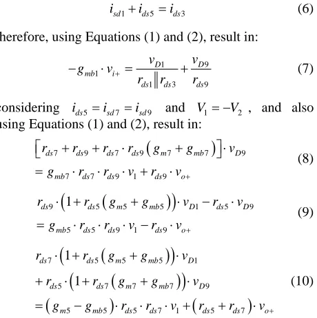
the DC-Gain, so before fabrication, the proposed ampli- fier must be simulated in the corners of fabrication proc- ess and wide temperature ranges. In this design proce- dure, K11.33 and K29.12 are obtained, respect- tively. Bias circuit and CMFB block which utilized in the conventional and proposed structures is shown in Fig- ures 3 and 4, respectively.
3. Simulation Results
In this section, simulation results of the proposed ampli- fier are shown and are compared with the conventional structure. Amplifiers have been designed in a typical 0.18 µm CMOS process with the same capacitor load and power consumption and then simulated by HSPICE en- vironment using level 49 parameters. A closed-loop con- figuration with 1 pF capacitors is used to study the line- arity and step response of the amplifiers, which is shown in Figure 5. With the mentioned value of capacitors, closed-loop gain of the amplifiers is approximately 0 dB. HSPICE AC simulation results of the proposed and the conventional FC amplifiers are shown in Figure 6. The UGBW and phase margin of both structures are ap- proximately equal. As demonstrated in Figure 6, the proposed amplifier achieves a DC-Gain about 50 dB which is 11 dB higher than DC-Gain of the conventional amplifier in the same power supply and process. It is considerable that by choosing a greater amount of both
1
Figure 3. Bias circuit for both amplifiers.
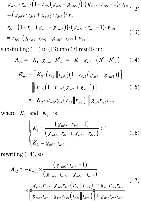
Figure 4. CMFB circuit for both amplifiers.
Figure 5. Closed-loop configuration.
[image:4.595.309.538.87.237.2]output voltage amplitudes. However, in higher output voltage amplitudes, both amplifiers have acceptable line- arity and eliminate undesirable harmonics. The accuracy of the amplifiers for different input step voltage ampli- tudes in unity gain configuration was also tested. The result of the step response simulation for 500 mV ampli- tude is illustrated in Figure 8, which demonstrate that the accuracy of the proposed amplifier is more than 8 bit for up to 500 mV output voltage swing.
[image:4.595.58.283.96.380.2]Figure 6. Open-loop frequency response of amplifiers.
Figure 7. THD comparison of amplifiers in different voltage swing.
[image:4.595.312.538.253.385.2]Figure 8. Step response of amplifiers for Vop-p = 500 mV.
Figure 9 illustrates the effective input transconductance of amplifiers as a function of the input CM voltage. It is obvious that both designs function correctly for rail-to- rail input CM voltage values with acceptable variations. Finally, the simulated performance of both amplifiers and its comparison with previous structures are summa- rized in Table 1. In order to compare the relative per- formance of structures, a new figure of merit (FOM) is used as follows:
-UGBW
FOM 20 log L V inp p
diss
A V
C
P THD
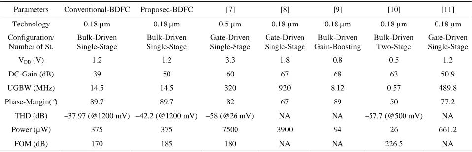
[image:4.595.309.537.425.560.2]Table 1. Comparisons of characteristics of proposed amplifier with conventional and previous amplifiers.
Parameters Conventional-BDFC Proposed-BDFC [7] [8] [9] [10] [11]
Technology 0.18 µm 0.18 µm 0.5 µm 0.18 µm 0.18 µm 0.18 µm 0.18 µm
Configuration/ Number of St.
Bulk-Driven Single-Stage
Bulk-Driven Single-Stage
Gate-Driven Single-Stage
Gate-Driven Single-Stage
Bulk-Driven Gain-Boosting
Bulk-Driven Two-Stage
Gate-Driven Single-Stage
VDD (V) 1.2 1.2 3.3 1.8 0.8 0.5 1.2
DC-Gain (dB) 39 50 60 67 68 63 50.9
UGBW (MHz) 14.5 14.5 320 920 8.12 0.57 489.8
Phase-Margin(°) 89.7 89.7 82 67 89 50 77.2
THD (dB) –37.97 (@1200 mV) –42.2 (@1200 mV) –58 (@26 mV) NA NA –57.7 (@500 mV) NA
Power (µW) 375 375 7500 3900 94 26 661.2
[image:5.595.58.537.101.256.2]FOM (dB) 170 185 180 NA NA 226.5 NA
Figure 9. Effective bulk-transconductance of amplifiers from rail-to-rail.
The unit of proposed FOM is
MHz pF mV
mW, which this form the benchmark for the comparison with the results from this work.4. Conclusions
In this paper, a novel approach to increase the DC-Gain of conventional BDFC amplifier is presented. With the presented method the DC-Gain of proposed amplifier increased more than 11 dB. All transistors in both ampli-fiers have same size and both designs consume 375 µW with 1 pF capacitive load.
Accuracy in the closed-loop configuration of amplifier in higher output voltage swings is the main advantage of the proposed structure. Step response simulations dem-onstrate that the accuracy of the proposed amplifier is more than 8 bit for up to 500 mV output voltages swing. Moreover, THD simulations show that proposed ampli-fier achieves reasonable linearity in comparison with conventional structure in different voltage swings, espe-cially in large input signal swing.
REFERENCES
[1] S. Chatterjee, Y. Tsvidis and P. Kinget, “Ultra-Low
Vol-tage Analog Integrated Circuits,” IEICE Transactions on Electronics, Vol. E89-C, No. 6, 2006, pp. 673-680. [2] S. Yan and E. Sanchez-Sinencio, “Low-Voltage Analog
Circuit Design Techniques: A Tutorial,” IEICE Transac-tions, Vol. E00-A, No. 2, 2000, pp. 179-196.
[3] J. Ramirez-Angulo, R. G Carvajal and A. Torralba, “Low Supply Voltage High Performance CMOS Current Mirror with Low Input and Output Voltage Requirements,” IEEE Transactions on Circuits and Systems-II Express Briefs, Vol. 51, No. 3, 2004, pp. 124-129.
doi:10.1109/TCSII.2003.822429
[4] ITRS, “The International Technology Roadmap for Sem-conductors,” 2008. http://public.itrs.net
[5] B. Razavi, “Design of Analog CMOS Integrated Circuits,” McGraw Hill, New York, 2001.
[6] P. R. Gray, P. J. Hurst, S. H. Lewis and R. G. Meyer, “Analysis and Design of Analog Integrated Circuits,” 4th Edition, John Wiley & Sons, New York, 2001.
[7] S. M. R. Hasan and N. Ula, “A Novel Feed-Forward Compensation Technique for Single-Stage Ful-ly-Differential CMOS Folded-Cascode Rail-to-Rail Am-plifier,” Electrical Engineering, Vol. 88, No. 6, 2006, pp. 509-517.
doi:10.1007/s00202-005-0306-2
[8] B. Alizadeh and A. Dadashi, “An Enhanced Folded-Cascode Op-Amp in 0.18 µm CMOS Process with 67 dB DC-Gain,” IEEE International Conference, Faible Tension Faible Consummation, 30 May-1 June 2011, pp. 87-90.
[9] J. Rosenfeld, M. Kozak and E. G. Friedman “A Bulk- Driven CMOS OTA with 68-dB DC-Gain,” Proceedings of IEEE International Electronics Circuits Systems, Tel- Aviv, 13-15 December 2004, pp. 5-8.
[10] M. Trakimas and S. Sonkusale, “A 0.5 V Bulk-Input OTA with Improved Common-Mode Feedback for Low-Frequency Filtering Applications,” Analog Inte-grated Circuits and Signal Processing, Vol. 59, No. 1, 2009, pp. 83- 89. doi:10.1007/s10470-008-9236-z