1
Faculty of Electrical Engineering,
Mathematics & Computer Science
Evaluating
Performance and Energy
Efficiency
of the
Hybrid Memory Cube Technology
ing. A.B. (Arvid) van den Brink
Master Thesis
August 2017
Exam committee:
Abstract
Embedded systems process fast and complex algorithms these days. Within these embedded systems, memory becomes a major part. Large (amount of bytes), small (in terms of area), fast and energy efficient memories are needed not only in battery operated devices but also in High Performance Computing systems to reduce the power consumption of the total system.
Many systems implement their algorithm in software, usually implying a sequential execution. The more complex the algorithm, the more instructions are executed and therefore the execution time and power consumption increases accordingly. Parallel execution can be used to compensate for the increase in execution time introduced by the sequential software. For parallel execution of regular, structured algorithms, hardware solutions, like an FPGA, can be used. Only the physical boundaries of FPGAs limits the amount of parallelism.
In this thesis a comparison is made between two systems. The first system is using the Hybrid Memory Cube memory architecture. The processing element in this system is an FPGA. The sec-ond system is a common of the shelf graphical card, containing GDDR5 memory with a GPU as processing unit.
The Hybrid Memory Cube memory architecture is used to give an answer to the main research question: ”How does the efficiency of the Hybrid Memory Cube compare to GDDR5 memory?”. The energy efficiency and the performance, in terms of speed, are compared to a common of the shelf graphical card. Both systems provide the user with a massively parallel architecture.
Two benchmarks are implemented to measure the performance of both systems. The first is the data transfer benchmark between the host system and the device under test and the second is the data transfer benchmark between the GPU and the GDDR5 memory (AMD Radeon HD7970) or the FPGA and the HMC memory. The benchmark results show an average speed performance gain of approximately5.5×in favour of the HMC system.
Due to defective HMC hardware, only power measurements are compared when both the graphical card and HMC system were in theIdle state. This resulted that the HMC system is approximately
Contents
Abstract i
List of Figures viii
List of Tables ix
Glossary xi
1 Introduction 1
1.1 Context . . . 1
1.2 Problem statement . . . 3
1.3 Approach and outline . . . 3
I Background
5
2 Related Work 7 3 Memory architectures 9 3.1 Principle of Locality . . . 93.2 Random Access Memory (RAM) memory cell . . . 10
3.3 Principles of operation . . . 12
3.3.1 Static Random Access Memory (SRAM) - Standby . . . 12
3.3.2 SRAM - Reading . . . 13
3.3.3 SRAM - Writing . . . 13
3.3.4 Dynamic Random Access Memory (DRAM) - Refresh . . . 13
3.3.5 DRAM - Reading . . . 14
3.3.6 DRAM - Writing . . . 15
3.4 Dual In-Line Memory Module . . . 15
3.5 Double Data Rate type 5 Synchronous Graphics Random Access Memory . . . 17
3.6 Hybrid Memory Cube . . . 19
3.6.1 Hybrid Memory Cube (HMC) Bandwidth and Parallelism . . . 25
3.6.2 Double Data Rate type 5 Synchronous Graphics Random Access Memory (GDDR5) versus HMC . . . 26
4 Benchmarking 29 4.1 Device transfer performance . . . 30
4.2 Memory transfer performance . . . 31
4.3.1 Median Filter . . . 31
5 Power and Energy by using Current Measurements 35 6 Power Estimations 39 6.1 Power Consumption Model for AMD Graphics Processing Unit (GPU) (Graphics Core Next (GCN)) . . . 40
6.2 Power Consumption Model for HMC and Field Programmable Gate Array (FPGA) . . . 41
II Realisation and results
43
7 MATLAB Model and Simulation Results 45 7.1 Realisation . . . 457.1.1 Image Filtering . . . 45
7.2 Results . . . 46
7.2.1 MATLAB results . . . 46
8 Current Measuring Hardware 47 8.1 Realisation . . . 47
8.2 Results . . . 48
9 GPU Technology Efficiency 51 9.1 Realisation . . . 51
9.1.1 Host/GPU system transfer performance . . . 51
9.1.2 GPU system local memory (GDDR5) transfer performance . . . 52
9.1.3 GPU energy efficiency test . . . 52
9.2 Results . . . 53
9.2.1 Host/GPU transfer performance . . . 53
9.2.2 GPU/GDDR5 transfer performance . . . 54
9.2.3 GDDR5 energy efficiency results . . . 55
10 Hybrid Memory Cube Technology Efficiency 57 10.1 Realisation . . . 57
10.1.1 Memory Controller Timing Measurements . . . 57
10.1.1.1 User Module - Reader . . . 58
10.1.1.2 User Module - Writer . . . 59
10.1.1.3 User Module - Arbiter . . . 60
10.1.2 Memory Controller Energy Measurements . . . 60
10.2 Results . . . 60
10.2.1 HMC performance results . . . 60
10.2.2 HMC energy efficiency results . . . 63
III Conclusions and future work
65
11 Conclusions 67 11.1 General Conclusions . . . 6711.2 HMC performance . . . 68
11.4 HMC improvements . . . 69
12 Future work 71 12.1 General future work . . . 71
12.2 Hybrid Memory Cube Dynamic power . . . 71
12.3 Approximate or Inexact Computing . . . 71
12.4 Memory Modelling . . . 71
IV Appendices
73
A Mathematical Image Processing 75 A.1 Image Restoration . . . 75A.1.1 Denoising . . . 75
A.1.1.1 Random noise . . . 75
B Arduino Current Measure Firmware 79
C Field Programmable Gate Array 81
D Test Set-up 85
E Graphics Processing Unit 87
F Riser Card 89
G Benchmark C++/OpenCL Code 93
H Image Denoising OpenCL Code 107
I MATLAB Denoise Code 109
Index 111
List of Figures
2.1 HMC module: AC510 board . . . 8
3.1 Temporal locality: Refer to block again . . . 9
3.2 Spatial locality: Refer nearby block . . . 9
3.3 Six transistor SRAM cell . . . 10
3.4 Four transistor SRAM cell . . . 11
3.5 SRAM cell layout: (a) A six transistor cell; (b) A four transistor cell . . . 11
3.6 One transistor, one capacitor DRAM cell . . . 11
3.7 One transistor, one capacitor cell . . . 12
3.8 Dual In-Line Memory Module memory subsystem organisation . . . 15
3.9 Dual In-Line Memory Module (DIMM) Channels . . . 16
3.10 DIMM Ranks . . . 16
3.11 DIMM Rank breakdown . . . 16
3.12 DIMM Chip . . . 17
3.13 DIMM Bank Rows and Columns . . . 17
3.14 Double Data Rate type 5 Synchronous Graphics Random Access Memory (GDDR5) . 18 3.15 Cross Sectional Photo of HMC Die Stack Including Through Silicon Via (TSV) Detail (Inset) [1] . . . 19
3.16 HMC Layers [2] . . . 19
3.17 Example HMC Organisation [3] . . . 20
3.18 HMC Block Diagram Example Implementation [3] . . . 21
3.19 Link Data Transmission Example Implementation [3] . . . 22
3.20 Example of a Chained Topology [3] . . . 23
3.21 Example of a Star Topology [3] . . . 23
3.22 Example of a Multi-Host Topology [3] . . . 24
3.23 Example of a Two-Host Expanded Star Topology [3] . . . 24
3.24 HMC implementation: (a) 2 Links; (b) 32 Lanes (Full width link) . . . 25
3.25 GDDR5 - Pseudo Open Drain (POD) . . . 26
4.1 Functional block diagram of test system . . . 29
4.2 Denoising example: (a) Original; (b) Impulse noise; (c) Denoised (3×3window) . . . 33
5.1 Current Sense Amplifier . . . 37
7.1 Median Filtering: (a) Boundary exceptions; (b) No Boundary exceptions . . . 45
7.2 MATLAB Simulation: (a) Original; (b) Impulse Noise; (c) Filtered (3x3); (d) Filtered (25x25) . . . 46
8.2 Test set-up: (a) Overview; (b) Riser card Printed Circuit Board (PCB) - with HMC
Backplane inserted . . . 48
8.3 Hall Sensor board ACS715 - Current Sensing . . . 48
8.4 Arduino Nano with an ATmega328p AVR . . . 48
8.5 AC715 Hall sensors readout - Power off . . . 50
9.1 Host to GPU Bandwidth . . . 53
9.2 GPU Local memory Bandwidth . . . 54
9.3 GPU Idle Power . . . 55
9.4 GPU Benchmark Power . . . 56
10.1 Hybrid Memory Cube Memory Controller - User Module Top Level . . . 58
10.2 User Module - Reader . . . 59
10.3 User Module - Writer . . . 59
10.4 Hybrid Memory Cube Giga-Updates Per Second . . . 61
10.5 Hybrid Memory Cube Bandwidth (9 user modules) . . . 62
10.6 Hybrid Memory Cube versus Double Data Rate type 3 Synchronous Dynamic Random Access Memory (DDR3) Bandwidth . . . 62
10.7 Hybrid Memory Cube Read Latency . . . 63
10.8 HMC Idle Power . . . 63
C.1 XCKU060 Banks . . . 81
C.2 XCKU060 Banks in FFVA1156 Package . . . 81
C.3 FFVA1156 PackageXCKU060 I/O Bank Diagram . . . 82
C.4 FFVA1156 PackageXCKU060 Configuration/Power Diagram . . . 83
D.1 Test Set-up block diagram . . . 85
E.1 AMD Radeon HD 7900-Series Architecture . . . 87
E.2 AMD Radeon HD 7900-Series GCN . . . 87
F.1 Riser card block diagram . . . 89
F.2 Riser card schematic - Current Sensing section . . . 89
List of Tables
3.1 RAM main operations . . . 12
3.2 Memory energy comparison . . . 27
4.1 PCIe link performance . . . 30
5.1 Current sensing techniques . . . 38
7.1 Median Filter Image Sizes . . . 46
8.1 AC715 Hall sensors average current - Power off . . . 49
9.1 Host to GPU Bandwidth . . . 53
9.2 GPU Local memory Bandwidth . . . 55
9.3 GPU Median Filter Metrics . . . 56
10.1 Hybrid Memory Cube Bandwidth (9 user modules) . . . 61
11.1 Memory Bandwidth Gain . . . 68
C.1 Kintex UltraScale FPGA Feature Summary . . . 84
Glossary
ADC Analog to Digital Converter
API Application Programming Interface
ASIC Application Specific Integrated Circuit
BFS Breadth-First Search
CAS Column Address Select
CBR CAS Before RAS
CK Command Clock
CMOS Complementary Metal Oxide Semiconductor
CMV Common-mode Voltage
CMR Common-mode Rejection
CNN Convolutional Neural Network
CPU Central Processing Unit
CSP Central Signal Processor
DDR Double Data Rate SDRAM
DDR3 Double Data Rate type 3 Synchronous Dynamic
Random Access Memory
DIMM Dual In-Line Memory Module
DLL Delay Locked Loop
DMA Direct Memory Access
DRAM Dynamic Random Access Memory
DSP Digital Signal Processing
DUT Device Under Test
DVFS Dynamic Voltage/Frequency Scaling
EOL End Of Life
FLIT Flow Unit
FPGA Field Programmable Gate Array
GCN Graphics Core Next
GDDR Double Data Rate Synchronous Graphics
Random Access Memory
GDDR5 Double Data Rate type 5 Synchronous Graphics Random Access Memory
GPU Graphics Processing Unit
GUPS Giga-Updates Per Second
HBM High Bandwidth Memory
HDL Hardware Description Language
HMC Hybrid Memory Cube
HPC High Performance Computing
HPCC HPC challenge
IC Integrated Circuit
I/O Input/Output
LFSR Linear Feedback Shift Register
LM Link Master
LS Link Slave
MCU Micro Controller Unit
MOSFET Metal-Oxide-Semiconductor Field-Effect Transistor
MRI Magnetic Resonance Imaging
ODT On-Die Termination
OpenCL Open Computing Language
P2P Point-To-Point
P22P Point-To-Two-Point
PC Personal Computer
PCB Printed Circuit Board
PCIe Peripheral Component Interconnect Express
PDF Probability Density Function
PLL Phase Locked Loop
POD Pseudo Open Drain
RAM Random Access Memory
RAS Row Address Select
ROR RAS Only Refresh
SDP Science Data Processor
SDRAM Synchronous Dynamic Random Access Memory
SGRAM Synchronous Graphics Random Access Memory
SKA Square Kilometre Array
SLID Source Link Identifier
SR Self Refresh
SRAM Static Random Access Memory
TSV Through Silicon Via
VHDL VHSIC (Very High Speed Integrated Circuit)
Hardware Description Language
WCK Write Clock
Chapter 1
Introduction
1.1 Context
Many embedded systems are using fast and complex algorithms to perform the designated task these days. The execution of these algorithms commonly requires a Central Processing Unit (CPU), memory and storage. Nowadays, memory becomes a major part of these embedded systems. The demand for larger memory sizes in increasingly smaller and faster devices requires a memory archi-tecture that occupies less area, performs at higher speeds and uses less power consumption. Not only in battery operated devices the power consumption is a key feature, also in High Performance Computing (HPC) systems the total power consumption is important. For example, a smartphone user wants to use the phone for many hours without the need of recharging the smartphone or like the HPC systems used for the international Square Kilometre Array (SKA) telescope [4] by one of its part-ners ASTRON [5], where the energy consumption is becoming a major concern as well. This HPC system consist of the Central Signal Processor (CSP) [6] and the Science Data Processor (SDP) [7] elements and many more. These elements consume multiple megawatts of power. Reducing the power consumption in these systems is as important as in mobile, battery powered devices.
To reduce the amount of energy used by a system, a new kind of memory architecture, like the Hybrid Memory Cube (HMC) [8], can be used. Despite the reduction in area and energy usage and the increase in speed, the rest of the system still uses the same computer architecture as the general purpose systems and therefore the system is not fully optimised for the execution of the same algorithms. Introducing an FPGA, to create optimised Digital Signal Processing (DSP) blocks, can also reduce the amount of energy and time needed for the complex tasks. The FPGA is a specialised Integrated Circuit (IC) containing predefined configurable hardware resources, likelogic blocks and DSPs. By configuring the FPGA, any arbitrary digital circuit can by made.
The computational power needed depends on the complexity of the executed algorithm. Using a general purpose CPU needs the algorithm to be described in software. This software is made up out of separate instructions which are usually executed in sequence. The more complex the algorithm, the more instructions needed for the execution, hence the execution time increases.
parallelism. More complex algorithms can require more resources than available in the FPGA. If a full parallel implementation does not fit in the FPGAsarea, pipelining1can be used to execute parts of the algorithm sequentially over time. The trade-off between resource usage and execution time is made by the developer.
The use of an FPGA can be seen as the trade-off between area and time as an FPGA can be configured specifically for the application it is used for. In the field of radio astronomy, like in other applications, many algorithms similar to image processing are seen. Image processing algorithms are very suitable for implementation on an FPGA due to the following properties:
• The algorithms are computationally complex
• Computations can potentially be performed in parallel
• Execution time can be guaranteed due to deterministic behaviour of the FPGA
As mentioned before image processing is essential in many applications, including astrophysics, surveillance, image compression and transmission, medical imaging and astronomy, just to name a few. Images in just one dimension are called signals. In two dimensions images are in the planar field and in three dimensions volumetric images are created, like Magnetic Resonance Imaging (MRI). These images can be coloured (vector-valued functions) or in gray-scale (single-value functions). Many types of imperfections, like noise and blur, in the acquired data often degrade the image. Before any feature extraction and further analysis is done, the images have to be first pre-processed.
In this research on energy efficiency of the HMC architecture, image denoising will be used. The technique used is the Median filter. Because this image processing algorithm, like most image pro-cessing algorithms, is highly complex and is executed on a fast amount of data, the combination of the HMC technology and FPGAs seems a logical choice.
The configuration of an FPGA can be done with a Hardware Description Language (HDL). Due to the possible parallelism in the hardware and the lower clock frequency of the FPGA in comparison to a CPU, in combination with HMC memory, a much lower energy consumption and execution time can possibly be obtained. To describe the hardware architecture, languages like VHSIC (Very High Speed Integrated Circuit) Hardware Description Language (VHDL) and Verilog are used. The manual work required is cumbersome.
Another framework is Open Computing Language (OpenCL). OpenCL is a framework for writing programs that execute across heterogeneous platforms consisting of CPUs, GPUs, DSPs, FPGAs and other processors or hardware accelerators. OpenCL specifies a programming language (based on C99) for programming these devices and Application Programming Interfaces (APIs) to control the platform and execute programs on the compute devices. OpenCL provides a standard interface for parallel computing using task-based and data-based parallelism.
1A pipeline is a set of processing elements connected in series, where the output of one element is the input of the next.
1.2 Problem statement
To evaluate the efficiency of the HMC, it is necessary to use a benchmark which can also run on other memory architectures, like GDDR5. The benchmark will provide the following metrics:
• Achievable throughput/latency (performance); • Achievable average power consumption.
This research will attempt to answer the following questions:
• What is the average power consumption and performance of the HMC? • How does the power consumption of the HMC compare to GDDR5 memory? • How does the performance of the HMC compare to GDDR5 memory? • What are the bottlenecks and (how) can this be improved?
Realising a hardware solution for mathematically complex and memory intensive algorithms has potential advantages in terms of energy and speed. To analyse these advantages, a solution on an FPGA driven Hybrid Memory Cube architecture is realised and compared to a similar OpenCL software solution on a GPU. The means to answer the research questions are summarised into the following statements:
• How to realise a feasible image denoising implementation on an FPGA and HMC? • How to realise a feasible image denoising implementation on a GPU?
• How to realise a feasible benchmark to compare the GPU with the FPGA and HMC?
• Does the FPGA and HMC implementation have the potential to be more energy and perfor-mance efficient compared to the GPU solution?
1.3 Approach and outline
Image denoising can be solved in different ways. To realise one solution that fits on both the FPGA/HMC and the GPU this solution must first be determined. This one solution must be imple-mented in Hardware Description Language (HDL) and in software. CλaSH is suitable for formulating complex mathematical problems and transforming this formulation into VHDL or Verilog HDL, but OpenCL is also supported for both the HMC and GPU architectures.
Part I - Background, contains the information on the different topics used in the research. Chapter 3 describes the different memory architectures of the memory modules used. Chapter 4 introduces the basic concepts regarding memory and CPU/GPU/FPGA benchmarking.
Part II - Realisation and results, shows the realised solutions and the results found.
Part I
Chapter 2
Related Work
Since the Hybrid Memory Cube is a fairly new memory technology, little has been studied on the impact on performance and energy efficiency. As an HMC I/O interface can achieve an external bandwidth up to480GB/s, using high-speed serial links, this comes at a cost. The static power of the off-chip links is largely dominating the total energy consumption of the HMC. As proposed by Ahn et al. [9] the use of dynamic power management for the off-chip links can result in an average energy consumption reduction of 51%.
Another study by Wang et al. [10] proposes to deactivate the least used HMCs and using erasure codes to compensate for the relatively long wake-up time of over2µs.
In 2014 Rosenfeld [11] defended his PhD thesis on the performance exploration of the Hybrid Memory Cube (HMC). For his research he used only simulations of the HMC architecture.
Finally, a paper by Zhu, et al. [12], discusses that GPUs are widely used to accelerate data-intensive applications. To improve the performance of data-data-intensive applications, higher GPU mem-ory bandwidth is desirable. Traditional Double Data Rate Synchronous Graphics Random Access Memory (GDDR) memories achieve higher bandwidth by increasing frequency, which leads to exces-sive power consumption. Recently, a new memory technology called High Bandwidth Memory (HBM) based on 3D die-stacking technology has been used in the latest generation of GPUs developed by AMD, which can provide both high bandwidth and low power consumption with in-package stacked DRAM memory, offering> 3×the bandwidth per watt of GDDR51. However, the capacity of
inte-grated in-packaged stacked memory is limited (e.g. only 4GB for the state-of-the-art HBM-enabled GPU, AMD Radeon Fury X [13], [14]). In his paper, Zhu et al. implement two representative data-intensive applications, Convolutional Neural Network (CNN) and Breadth-First Search (BFS) on an HBM-enabled GPU to evaluate the improvement brought by the adoption of the HBM, and investigate techniques to fully unleash the benefits of such HBM-enabled GPU. Based on his evaluation results, Zhu et al. first propose a software pipeline to alleviate the capacity limitation of the HBM for CNN. They then designed two programming techniques to improve the utilisation of memory bandwidth for the BFS application. Experiment results demonstrate that the pipelined CNN training achieves a 1.63x speed-up on an HBM enabled GPU compared with the best high-performance GPU on the
1Testing conducted by AMD engineering on the AMD Radeon R9 290X GPU vs. an HBM-based device. Data obtained
through isolated direct measurement of GDDR5 and HBM power delivery rails at full memory utilisation. Power efficiency
calculated as GB/s of bandwidth delivered per watt of power consumed. AMD Radeon R9 290X (10.66GB/sbandwidth per
watt) and HBM-based device (35 +GB/sbandwidth per watt), AMD FX-8350, Gigabyte GA-990FX-UD5, 8GB DDR3-1866,
market, and the two, combined optimisation techniques for the BFS algorithm makes it at most 24.5x (9.8x and 2.5x for each technique, respectively) faster than conventional implementations.
[image:22.595.229.339.208.444.2]At the time of writing this report, the Hybrid Memory Cube technology is, as far as known, only used in two applications. The first implementation is the HMC produced by Micron (formerly Pico-Computing) [15], [16], see figure 2.1. This module is used for the experiments in order to get the performance and power measurements, which are discussed in the rest of this thesis.
Figure 2.1: HMC module: AC510 board
Chapter 3
Memory architectures
It was predicted by computer pioneers that computer systems and programmers would want un-limited amounts of fast memory. Amemory hierarchy is an economical solution to that desire, which takes advantage of trade-offs and locality in the cost-performance of current memory technologies. Most programs do not access all code or data uniformly, as stated by the Principle of Locality. Local-ity occurs in space (spatial localLocal-ity) and in time (temporal locality). Moreover, for a given technology and power budget smaller hardware can be made faster, led to hierarchies based on memories of different sizes and speeds.
3.1 Principle of Locality
When executing a program on a computer, this program tends to use instructions and read or write data with addresses near or equal to those used recently by that program. The Principle of Locality, also known as theLocality of Reference, is the phenomenon of the same value or related storage locations being frequently accessed. There are two types of locality:
• Temporal locality: refers to the reuse of specific data and/or resources within relatively small time durations.
Figure 3.1: Temporal locality: Refer to block again
• Spatial locality: refers to the use of data elements within relatively close storage locations. Sequential locality, a special case of spatial locality, occurs when data elements are arranged and accessed linearly, e.g. traversing the elements in a one-dimensional array.
Figure 3.2: Spatial locality: Refer nearby block
memory location during a short time period. Both forms of locality occur in the following code snip-pet:
sum = 0;
f o r ( i = 0; i < n ; i ++) sum += a [ i ] ;
r e t u r n sum ;
In the above code snippet, the variable iis referenced several times in the for loop where iis
compared againstn, to see if the loop is complete, and also incremented by one at the end of the
loop. This showstemporallocality of reference in action since the CPU accessesiat different points
in time over a short period of time.
This code snippet also exhibits spatial locality of reference. The loop itself adds the elements of arrayato variablesum. Assuming C++ stores elements of arrayainto consecutive memory locations,
then on each iteration the CPU accesses adjacent memory locations.
3.2 RAM memory cell
SRAM is a type of semiconductor memory that usesflip-flopsto store a single bit. SRAM exhibits data remanence (keeping its state after writing or reading from the cell) [19], but it is still volatile. Data is eventually lost when the memory is powered off.
The term static differentiates SRAM from DRAM which must be periodically refreshed. SRAM is faster but more expensive than DRAM, hence it is commonly used for CPU cache while DRAM is typically used for main memory. The advantages of SRAM over DRAM are lower power consumption, simplicity (no refresh circuitry is needed) and reliability. There are also some disadvantages: a higher price and lower capacity (amount of bits). The latter disadvantage is due to the design of an SRAM cell.
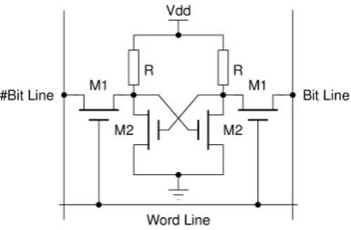
A typical SRAM cell is made up of six Metal-Oxide-Semiconductor Field-Effect Transistors (MOS-FETs). Each bit in an SRAM (see figure 3.3) is stored on four transistors (M1, M2, M3 and M4). This cell has two stable states which are used to denote0and1. Two additional transistors (M5 and M6)
[image:24.595.207.364.612.732.2]are used to control the access to that cell during read and write operations.
A four transistor (4T) SRAM (see figure 3.4) is quite common in standalone devices, which is implemented in special processes with an extra layer of poly-silicon, allowing for very high-resistance pull-up resistors. The main disadvantage of using 4T SRAM is the increased static power due to the constant current flow through one of the pull-down transistors.
Figure 3.4: Four transistor SRAM cell
Generally, the fewer transistors needed per cell, the smaller each cell. Since the cost of processing a silicon wafer is relatively fixed, therefore using smaller cells and so packing more bits on a single wafer reduces the cost per bit. In figure 3.5a the layout of a 6T cell with dimensions5×PM etalby2×
PM etalis shown. A 4T cell, as can be seen in figure 3.5b, has only a dimension of5×PM etalby1.5×
PM etal. PM etaldenote the Metal Pitch used by the manufacturing process. The pitch is the centre to
centre distance between the metals, having minimal width and minimal spacing.
(a) (b)
Figure 3.5: SRAM cell layout: (a) A six transistor cell; (b) A four transistor cell
[image:25.595.217.410.152.278.2]To access the memory cell (see figure 3.3) the word line (WL) gives access to transistors M5 and M6 which, in turn, control whether the cell (cross-coupled inverters) should be connected to the bit lines(BL). These bit lines are used for both write and read operations. Although it is not strictly necessary to have two bit lines, the two signals (BLandBL) are typically provided in order to improve noise margins.
Opposed the the static SRAM, there is thedynamic DRAM cell (see figure 3.6). In this type of memory cell the data is stored in a separate capacitor within the IC. A charged capacitor denotes a 1 and discharged denotes a 0. However, a non-conducting transistor will always leak a small
amount, discharging the capacitor, and the information in the memory cell eventually fades unless the capacitors charge is refreshed periodically, henceDynamic in the name. The DRAM cell layout is even smaller as can be seen in figure 3.7
Figure 3.7: One transistor, one capacitor cell
The structural simplicity is DRAMs advantage. Compared to the four or even six transistors re-quired in SRAM, just one transistor and one capacitor is rere-quired per bit in DRAM. This allows for very high densities, billions of these 1T cells can fit on a single chip. On the other hand, due to its dynamicnature, DRAM consumes relatively large amounts of power.
3.3 Principles of operation
Both types of RAM architectures have three main operations:
SRAM DRAM
Standby No Operation Reading
Writing
Table 3.1: RAM main operations
Due to the volatile nature of the DRAM architecture there is a fourth main operation, calledRefresh
An SRAM cell has three different states: standby (the circuit is idle), reading (the data has been requested) or writing (updating the contents). SRAM operating in read mode and write modes should havereadability andwrite stability, respectively. Assuming a six transistor implementation, the three different operations work as follows:
3.3.1 SRAM - Standby
If the word line is not asserted, the transistors M5 and M6 disconnect the cell (M1,M2,M3and M4) from the bit lines. The two cross-coupled inverters in the cell will continue to reinforce each other
3.3.2 SRAM - Reading
In theory, reading only requires asserting the word line andreadingthe SRAM cell state by a single access transistor and bit line, e.g.M6/BLandM5/BL. Nevertheless, bit lines are relatively long and have large parasitic capacitance. To speed up reading, a more complex process is used in practice: 1. Pre-charge both bit linesBLandBL, that is, driving both lines to a threshold voltage midrange
between a logic1and0by an external circuitry (not shown in figure 3.3).
2. Assert the word lineW Lto enable both transistors M5 and M6. This causes theBLvoltage to either slightly rise (nMOS1transistor M3 isOFF and pMOS2transistor M4 isON) or drop (M3
ifONand M4OFF). Note that ifBLrises,BLdrops and vice versa.
3. A sense amplifier will sense the voltage difference between BL andBL to determine which line has the higher voltage and thus which logic value (0or1) is stored. A more sensitive sense
amplifier speeds up the read operation.
3.3.3 SRAM - Writing
To write to SRAM the following two steps are needed:
1. Apply the value to be written to the bit lines. If writing a1,BL= 1andBL= 0.
2. Assert the word lineW Lto latch in the value to be stored.
This operation works, because the bit line input-drivers are designed to be much stronger than the relatively weak transistors in the cell itself so they can easily override the previous state of the cross-coupled inverters. In practice, the nMOS transistors M5 and M6 have to be stronger than either bottom nMOS (M1/M3) or top pMOS (M2/M4) transistors. This is easily obtained as pMOS transistors are much weaker than nMOS when same sized. Consequently when one transistor pair (e.g. M3/M4) is only slightly overridden by the write process, the opposite transistors pair (M1/M2) gate voltage is also changed. This means that the M1 and M2 transistors can be easier overridden, and so on. Thus, cross-coupled inverters magnify the writing process.
3.3.4 DRAM - Refresh
Due to the charge leaking away out of the capacitor over time, this charge on the individual cells must be refreshed periodically. The frequency with which this refresh must occur depends on the silicon technology used to manufacture the memory chip and the design of the memory cell itself.
Each cell must be accessed and restored during a refresh interval. In most cases, refresh cycles involve restoring the charge along an entire row. Over the period of the entire interval, every cell in a row is accessed and restored. At the end of the interval, this process begins again.
Memory designers have a lot of freedom in designing and implementing memory refresh. One choice is to fit the refresh cycles between normal read and write cycles, another is to run refresh cycles on a fixed schedule, forcing the system to queue read/write operations when they conflict with the refresh requirements.
1n-type MOSFET. The channel in the MOSFET contains electrons
Three common refresh options are briefly described below:
• RAS Only Refresh (ROR)3
Normally, DRAMs are refreshed one row at a time. The refresh cycles are distributed across the refresh interval so that all rows are refreshed within the required time period. Refreshing one row of DRAM cells using ROR, occurs in the following steps:
– The address of the row to be refreshed is applied at the address pins
– RAS is switched fromHightoLow. CAS4must remainHigh
– At the end of the, by specification, required amount of time, RAS is switch toHigh • CAS Before RAS (CBR)
Like RAS Only Refresh, CBR refreshes one row at a time. Refreshing a row using CAS Before RAS, occur in the following steps:
– CAS is switched fromHightoLow
– WE5is be switched toHigh(Read).
– After a specified required amount of time, RAS is switch toLow
– An internal counter determines the row to be refreshed
– After a specified required amount of time, CAS is switch toHigh
– After a specified required amount of time, RAS is switch toHigh
The main difference between CBR and ROR is the way for keeping track of the row address, respectively an internal counter or externally supplied.
• Self Refresh (SR)
Also known asSleep Modeor Auto Refresh. SR is a unique method of refresh. It uses an on-chip oscillator to determine the refresh rate and, like the CBR method, an internal counter to keep track of the row address. This method is frequently used for battery-powered mobile applications or applications that uses a battery for backup power.
The timing required to initiate SR is a CBR cycle with RAS active for a minimum amount of time as specified by the manufacturer. The length of time that a device can be left insleep modeis limited by the power source used. To exit, RAS and CAS are assertedHigh.
3.3.5 DRAM - Reading
To read from DRAM the following eight steps are needed: 1. Disconnect the sense amplifiers
2. Pre-charge the bit lines (differential pair) to exactly equal voltages that are midrange between logicalHighandLow. (E.g.0.5V in the case of ’0’= 0V and ’1’= 1V)
3. Turn off the pre-charge circuitry. The parasitic capacitance of the ”long” bit lines will maintain the charge for a brief moment
4. Assert a logic1at the word lineW Lof the desired row. This causes the transistor to conduct, enabling the transfer of charge to or from the capacitor. Since the capacitance of the bit line is typically much larger than the capacitance of the capacitor, the voltage on the bit line will slightly decrease or increase. (E.g. 0.45V=’0’ or0.55V=’1’). As the other bit line will stay at 0.5V there is a small difference between the two bit lines
3RAS: Row Address Select
4CAS: Column Address Select
5. Reconnect the sense amplifiers to the bit lines. Due to the positive feedback from the cross-connected inverters in the sense amplifiers, one of the bit lines in the pair will be at the lowest voltage possible and the other will be at the maximum high voltage. At this point the row isopen (the data is available)
6. All cells in theopenrow are now sensed simultaneously, and the sense amplifier outputs are latched. A column address selects which latch bit to connect to the external data bus. Read-ing different columns in the same (open) row can be performed without a row openRead-ing delay because, for the open row, all data has already been sensed and latched
7. While reading columns in anopenrow is occurring, current is flowing back up the bit-lines from the output of the sense amplifiers and recharging the cells. This reinforces (”refreshes”) the charge in the cells by increasing the voltage in the capacitor (if it was charged to begin with), or by keeping it discharged (if it was empty).
Note that, due to the length of the bit lines, there is a fairly long propagation delay for the charge to be transferred back to the cells capacitor. This takes significant time past the end of sense amplification and thus overlaps with one or more column reads
8. When done with reading all the columns in the currentopenrow, the word line is switchedOff to disconnect the cell capacitors (the row is ”closed”) from the bit lines. The sense amplifier is switchedOff, and the bit lines are pre-charged again (Next read starts from item 3).
3.3.6 DRAM - Writing
To store data, a row is opened and a given column sense amplifier is temporarily forced to the desiredLow or Highvoltage, thus causing the bit line to discharge or charge the cells capacitor to the desired value. Due to the sense amplifiers positive feedback configuration, it will hold a bit line at a stable voltage even after the forcing voltage is removed. During a write to a particular cell, all the columns in that row are sensed simultaneously (just as during reading), so although only a single columns cell capacitor charge is changed, the entire row isrefreshed.
[image:29.595.246.381.535.691.2]3.4 Dual In-Line Memory Module
Figure 3.8: Dual In-Line Memory Module memory subsystem organisation
are one or more DIMMs (see figure 3.9). The DIMM contains the actual DRAM chips that provide 4 or 8 bits of data per chip.
Figure 3.9: DIMM Channels
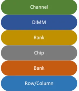
Current CPUs support triple or even quadruple channels. These multiple, independent channels increase data transfer rates due to the concurrent access of multiple DIMMs. Due to interleaving, latency is reduced when operating in triple-channel or in quad-channel mode. The memory controller distributes the data amongst the DIMMs in an alternating pattern, allowing the memory controller to access each DIMM for smaller bits of data instead of accessing a single DIMM for the entire chunk of data. This provides the memory controller more bandwidth for accessing the same amount of data across channels instead of traversing a single channel when it stores all data in one DIMM.
The Dual Inline of the DIMM refers to the DRAM chips on both sides of the module. The ”group” of chips on one side of the DIMMis called aRank (see figure 3.10). BothRankson the DIMM can be accessed simultaneously by the memory controller. Within a single memory cycle 64 bits of data is accessed. These 64 bits may come from the 8 or 16 DRAM chips, depending on the data width of a single chip (see figure 3.11).
Figure 3.10: DIMM Ranks
Figure 3.11: DIMM Rank breakdown
two chunks on each side. To increase capacity, combine the ranks with the largest DRAM chips. A quad-ranked DIMM with4Gbchips equals16GBDIMM (4Gb×8chips×4ranks/8bits).
Figure 3.12: DIMM Chip
Finally, the DRAM chip is made up of severalbanks(see figure 3.12). These banks are indepen-dent memory arrays which are organised in rows and columns (see figure 3.13).
Figure 3.13: DIMM Bank Rows and Columns
For example, a DRAM chip with13 address bits for Row selection, 10 address bits forColumn selection,8Banksand8bits per addressable location, this chip has a total density of2Rows·2Cols·
Banks·BitsAddressable= 213·210·8·8 = 512Mbit (64M x8bits).
3.5 Double Data Rate type 5 Synchronous Graphics Random
Access Memory
GDDR5 is the most commonly used type of Synchronous Graphics Random Access Memory (SGRAM) at the moment of writing this thesis. This type of memory has a highbandwidth(Double Data Rate SDRAM (DDR)) interface for use in HPC and graphics cards.
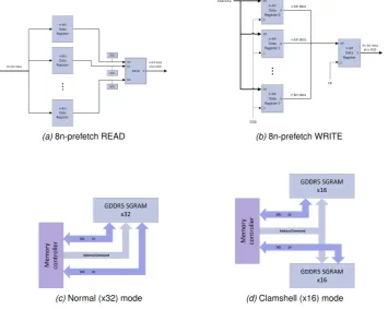
GDDR5 uses a DDR3 interface and an 8n-prefetch architecture (see figures 3.14a and 3.14b) to achieve high performance operations. The prefetch buffer depth (8n) can also be thought of as the ratio between the core memory frequency and the Input/Output (I/O) frequency. In an 8n-prefetch architecture, the I/Os will operate 8×faster than the memory core (each memory access results in
a burst of 8 datawords on the I/Os). Thus a200M Hzmemory core is combined with I/Os that each operate eight times faster (1600megabits per second). If the memory has 16I/Os, the total read
bandwidth would be200M Hz×8datawords/access×16I/Os= 25.6Gbit/s, or3.2GB/s. At Power-up, the device is configured inx32 mode or inx16 clamshell mode, where the 32-bit I/O, instead of being connected to one IC, is split between two ICs (one on each side of the PCB), allowing for a doubling of the memory capacity.
Just by adding additional DIMMs to the memory channels is the traditional way of increasing mem-ory density in PC and server applications. However, this dual-rank configuration can lead to perfor-mance degradation resulting from the dual-load signal topology (The databus is share by both ranks). GDDR5 uses a single-loaded or Point-To-Point (P2P) data bus for the best performance.
GDDR5 devices are always directly soldered on the PCB and are not mounted on a DIMM. Inx16 mode, the data bus is split into two 16-bit wide buses that are routed separately to each device (see figure 3.14d). The Address andCommand pins are shared between the two devices to preserve the total I/O pin count at the controller. However, this Point-To-Two-Point (P22P) topology does not decrease system performance because of the lower data rates of the address or command bus.
(a)8n-prefetch READ (b)8n-prefetch WRITE
[image:32.595.109.465.413.696.2](c)Normal (x32) mode (d)Clamshell (x16) mode
Figure 3.14: Double Data Rate type 5 Synchronous Graphics Random Access Memory (GDDR5)
data reads and writes, that runs at twice the CK frequency. A Delay Locked Loop (DLL) circuit is driven from the clock inputs and output timing for read operations is synchronised to the input clock. Being more precise, the GDDR5 SGRAM uses a total of three clocks:
1. Two write clocks associated with two bytes: WCK01 and WCK23 2. One Command Clock (CK)
Over the GDDR5 interface 64-bits of data (two 32-bit wide data words) per WCK can be transferred. Corresponding to the 8n-prefetch, a single write or read access consists of a 256-bit wide two CK clock cycle data transfer at the internal memory core and eight corresponding 32-bit wide one-half WCK clock cycle data transfers at the I/O pins.
Taking a GDDR5 with5Gbit/s data rate per pin as an example, the CK runs with1.25GHz and both WCK clocks at 2.5GHz. The CK and WCKs are phase aligned during the initialisation and training sequence. This alignment allows read and write access with minimum latency.
3.6 Hybrid Memory Cube
As written in [20] the Hybrid Memory Cube combines several stacked DRAM dies on top of a Complementary Metal Oxide Semiconductor (CMOS) logic layer forming a so called cube. The combination of both DRAM technology and CMOS technology dies makes this ahybridchip, hence the name Hybrid Memory Cube. The dies in the 3D stack are connected by means of a dense interconnect mesh of Through Silicon Vias (TSVs), which are metal connections extending vertically through the entire stack (see figures 3.15 and 3.16).
Figure 3.15: Cross Sectional Photo of HMC Die Stack Including TSV Detail (Inset) [1]
Unlike conventional DDR3 DIMM which has the electrical connection through the pressure of the pins in the connector, the TSVs form a permanent connection between all the layers in the stack. The TSV connections provide a very short (less then ammup to a fewmm) with less capacitance than the long PCB trace buses which can extent to manycm, hence data can be transmitted at a reasonable high data rate through the HMC stack without the use of power hungry and expensive I/O drivers [21].
[image:34.595.170.397.336.554.2]Within each HMC [3], memory is vertically organised. A partition of each memory die is combined into a vault (see figure 3.17). Each vault is operationally and functionally independent. The base of a vault contains a vault controller located in the CMOS die. The role of the vault controller is like a traditional memory controller in that it sends DRAM commands to the memory partitions in the vault and keeps track of the memory timing constraints. The communication is through the TSVs. A vault is more or less equivalent to a conventional DDR3 channel. However, unlike traditional DDR3 memory, the TSV connections are much shorter than the conventional bus traces on a motherboard and therefore have much better electrical properties. An illustration of the architecture can be seen in figure 3.17.
Figure 3.17: Example HMC Organisation [3]
The vault controller, by definition, may have a queue to buffer references inside that vaults memory. The execution of the references within the queue may be based on need rather than the order of ar-rival. Therefore the response from the vault to the external serial I/O links will be out of order. When no queue is implemented and two successive packets have to be executed on the same bank, the vault controller must wait for the bank to finish its operation, before the next packet can be executed, potentially blocking packet executions to other banks inside that vault. The queue can potentially optimise the memory bus usage.
The functions managed by the logic base of the HMC are:
• All HMC I/O, implemented as multiple serialised, full duplex links
• Memory control for each vault; Data routing and buffering between I/O links and vaults • Consolidated functions removed from the memory die to the controller
• Mode and configuration registers • BIST for the memory and logic layer
• Test access port compliant to JTAG IEEE 1149.1-2001, 1149.6
• Some spare resources enabling field recovery from some internal hard faults.
[image:35.595.180.449.262.499.2]A block diagram example for an implementation of a 4-link HMC configuration is shown in figure 3.18.
Figure 3.18: HMC Block Diagram Example Implementation [3]
Commands and data are transmitted in both directions across the link using a packet based proto-col where the packets consist of 128-bit Flow Units (FLITs). These FLITs are serialised, transmitted across the physical lanes of the link, then re-assembled at the receiving end of the link. Three con-ceptual layers handle packet transfers:
• The physical layer handles serialisation, transmission, and de-serialisation
• The link layer provides the low-level handling of the packets at each end of the link.
• The transaction layer provides the definition of the packets, the fields within the packets, and the packet verification and retry functions of the link.
Two logical blocks exist within the link layer and transaction layer (see figure 3.19):
• The Link Master (LM), is the logical source of the link where the packets are generated and the transmission of the FLITs is initiated.
The nomenclature below is used throughout this report to distinguish the direction of transmission between devices on opposite ends of a link. These terms are applicable to both host-to-cube and cube-to-cube configurations.
Requester:Represents either a host processor or an HMC link configured as a pass-through link. A requester transmits packets downstream to the responder.
[image:36.595.103.469.197.425.2]Responder:Represents an HMC link configured as a host link (See figure 3.20 through figure 3.23). A responder transmits packets upstream to the requester.
Figure 3.19: Link Data Transmission Example Implementation [3]
Multiple HMC devices may be chained together to increase the total memory capacity available to a host. A network of up to eight HMC devices and 4 host source links is supported, as will be explained in the next paragraphs. Each HMC in the network is identified through the value in its CUB field, located within the request packet header. The host processor must load routing configuration information into each HMC. This routing information enables each HMC to use the CUB field to route request packets to their destination.
Each HMC link in the cube network is configured as either a host linkor apass-through link, depending upon its position within the topology. See figure 3.20 through figure 3.23 for illustrations.
Ahost linkuses its Link Slave to receive request packets and its Link Master to transmit response packets. After receiving a request packet, the host link will either propagate the packet to its own internal vault destination (if the value in the CUB field matches its programmed cube ID) or forward it towards its destination in another HMC via a link configured as a pass-through link. In the case of a malformed request packet whereby the CUB field of the packet does not indicate an existing CUBE ID number in the chain, the request will not be executed, and a response will be returned (if not posted) indicating an error.
Figure 3.20: Example of a Chained Topology [3]
Figure 3.22: Example of a Multi-Host Topology [3]
An HMC link connected directly to the host processor must be configured as a host link in source mode. The Link Slave of the host link in source mode has the responsibility to generate and insert a unique value into the Source Link Identifier (SLID) field within the tail of each request packet. The unique SLID value is used to identify the source link for response routing. The SLID value does not serve any function within the request packet other than to traverse the cube network to its destination vault where it is then inserted into the header of the corresponding response packet. The host processor must load routing configuration information into each HMC. This routing information enables each HMC to use the SLID value to route response packets to their destination. Only a host link in source mode will generate an SLID for each request packet. On the opposite side of a pass-through link is a host link that is not in source mode. This host link operates with the same characteristics as the host link in source mode except that it does not generate and insert a new value into the SLID field within a request packet. All LSs in pass-through mode use the SLID value generated by the host link in source mode for response routing purposes only. The SLID fields within the request packet tail and the response packet header are considered Don’t Care” by the host processor. See figure 3.20 through figure 3.23 for illustrations for supported multi-cube topologies.
3.6.1 HMC Bandwidth and Parallelism
As mentioned in the previous section, a high bandwidth connection within each vault is available by using the TSVs to interconnect the 3D stack of dies. The combination of the number of TSVs (the density per cube can be in the thousands) and the high frequency at which data can be transferred provides a high bandwidth.
Because of the number of independent vaults in an HMC, each build up out of one or more banks (as in DDR3 systems), a high level of parallelism inside the HMC is achieved. Since each vault is roughly equivalent to a DDR3 channel and with 16 or more vaults per HMC, a single HMC can support an order of magnitude more parallelism within a single package. Furthermore, by stacking more dies inside a device, a greater number of banks per package can be achieved, which in turn is beneficial to parallelism.
The overall build up of the HMC, depending on the cubes configuration, can deliver an aggregate bandwidth of up to480GB/s(see figure 3.24).
(a) (b)
The available total bandwidth on an 8 Links, Full width HMC implementation is calculated as fol-lows:
• 15 Gb/s per Lane • 32 Lanes = 4 Bytes
• 8 Links / Cube = 480 GB/s / Cube
For the AC-510 [16] UltraScale-based SuperProcessor with HMC, providing 2 half width links, the total available bandwidth is equal to15Gb/s×2×2 = 60GB/s
3.6.2 GDDR5 versus HMC
To reduce the power consumption of GDDR5 many techniques have been employed. A POD signalling scheme, combined with an On-Die Termination (ODT) resistor [22] will only consume static power when drivingLOW as can be seen in figure 3.25.
Lowering the supply voltage (≈1.5V) of the memory, Dynamic Voltage/Frequency Scaling (DVFS) and the usage of independent ODT strength control of the command, address and data lines, are some of the other techniques used in GDDR5 memory. The DVFS [23] technique reduces power by adapting the voltage and/or the frequency of the memory interface while satisfying the throughput requirements of the application. However, this reduction in power results in the degradation of the throughput.
[image:40.595.203.370.478.631.2]Using all these techniques, to get a maximum throughput or bandwidth of6.0Gbpsa relatively high clock frequency is needed. For example, the memory clock of the AMD Radeon(tm) HD 7970 GHz edition GPU is equal to1500M Hz.
Figure 3.25: GDDR5 - Pseudo Open Drain (POD)
The architecture of the HMC, in contrast to GDDR5, uses some different techniques to reduce the power consumption. The supply voltage is reduced even more to only1.2V, and the clock frequency is reduced to only125M Hz, which is12times lower then that of the GDDR5 memory. To keep the
The above optimisations result in the following comparison. Note that in table 3.26not only GDDR5
and HMC memory, but also other memory architectures are included. The claim of the Hybrid Mem-ory Cube (HMC) consortium [8] that the HMC memMem-ory is≈66.5% more energy efficient per bit than
DDR3 memory, is concluded from this table. However, comparing the energy efficiency of the HMC to GDDR5 memory, the HMC is only≈17.6% more energy efficient per bit.
Technology VDD IDD Data rate Bandwidth Power Energy
(V) (A) (MT/s)7 (GB/s) (W) pJ/Byte pJ/bit
SDRAM PC133 1GB Module 3.3 1.50 133 1.06 4.95 4652.26 581.53 DDR-333 1GB Module 2.5 2.19 333 2.66 5.48 2055.18 256.90 DDRII-667 2GB Module 1.8 2.88 667 5.34 5.18 971.51 121.44 GDDR5 - 3GB Module 1.5 18.48 33000 264.00 27.72 105.00 13.13 DDR3-1333 1GB Module 1.5 1.84 1333 10.66 2.76 258.81 32.35 DDR4-2667 4GB Module 1.2 5.50 2667 21.34 6.60 309.34 38.67 HMC, 4 DRAM 1Gb w/ logic 1.2 9.23 16000 128.00 11.08 86.53 10.82
Table 3.2: Memory energy comparison
In table 3.2 the relation between the data rate and the bandwidth is:
bandwidth=DDR clock rate×bits transferred per clock cycle/8
Memory modules currently used are 64-bit devices. This means that 64 bits of data are transferred at each transfer cycle. Therefore,64 will be used as bits transferred per clock cycle in the above formula. Thus, the above formula can be simplified even further:
bandwidth=DDR clock rate×8
6The values forV
DD,IDDand Data rate can be found in the datasheets of the given memories.
Chapter 4
Benchmarking
[image:43.595.93.536.349.730.2]In order to compare GDDR5 and HMC memory, it is important to look at the performance and power consumption of these memory types. Because, in a complete system, not only the GDDR5 or HMC will be used, but also a GPU or FPGA, the comparison is made on a graphical card versus the HMC system [15] (see figure 4.1).
In the next sections a description of some of the key performance characteristics of a HMC and GDDR5 are given. This should give insight into the relative merits of using either an FPGA in combi-nation with the HMC memory or a GPU in combicombi-nation with the GDDR5 memory.
There is a vast array of benchmarks to choose from, but for this comparison this is narrowed down to three tests1, e.g. there will be no gaming and virtual reality benchmarking needed (see figure 4.1):
• How fast can data be transferred between the Personal Computer (PC) (host) and the graphical card (device 2) or HMC card (device 2)?
• How fast can the FPGA or GPU read and write data from HMC or GDDR5 respectively? • How fast can the FPGA or GPU read data from, do computations and write the result to HMC
or GDDR5 respectively?
In these benchmarks, each test is repeated up-to a hundred times to allow for other activities going on on the host and/or to eliminate the first-call overheads. During the repetition of the tests the overall minimum execution time per benchmark is kept as result, because external factors can only ever slow down execution. In the end this results in a maximum bandwidth. In order to get as close to an absolute performance measurement, it is important the host system execute as little tasks as possible.
4.1 Device transfer performance
This test measures how quickly the host can send data to and read data from the device (either HMC or GDDR5) (see figure 4.1). Since the device is plugged into the PCIe bus, the performance is largely dependent on the PCIe bus revision (see table 4.1) and how many other devices are con-nected to the PCIe bus. However, there is also some overhead that is included in the measurements, particularly the function call overhead and the array allocation time. Since these are present in any ”real world” use of the device, it is reasonable to include these overheads.
Note that the PCIe rev 3.0, is used in the test equipment, it has a theoretical bandwidth of1.0GB/s per lane. For the 16-lane slots (PCIe x16) used by the devices a maximum theoretical bandwidth of
16GB/sis given. Although an x16 slot is used, most of the devices only use 8 lanes and therefore the maximum theoretical bandwidth is only8GB/s.
PCI Express Transfer Throughput
version rate2 x1 x4 x8 x16
1.0 2.5 GT/s 250 MB/s 1 GB/s 2 GB/s 4 GB/s
2.0 5 GT/s 500 MB/s 2 GB/s 4 GB/s 8 GB/s
3.0 8 GT/s 984.6 MB/s 3.938 GB/s 7.877 GB/s 15.754 GB/s
4.0 (expected 2017) 16 GT/s 1.969 GB/s 7.877 GB/s 15.754 GB/s 31.508 GB/s 5.0 (far future) 25/32 GT/s 3.9/3.08 GB/s 15.8/12.3 GB/s 31.5/24.6 GB/s 63.0/49.2 GB/s
Table 4.1: PCIe link performance
1For all performance tests, also power consumption will be measured.
4.2 Memory transfer performance
While not all data is sent-to or read-from the PCIe bus, but can be processed ’locally’ using a GPU or FPGA (see figure 4.1), a separate test for measuring the Memory transfer performance should be executed. As many operations performed will do little computation with each data element of an array, these operations are therefore dominated by the time taken to fetch the data from memory or write it back to memory. Simple operators likeplus (+)orminus (-)do very little computation per
element that they are bound only by the memory access speed.
To know whether the obtainedmemory transfer benchmark figures are fast or not, the benchmark is compared with the same code running on a CPU reading and writing data to the main DDR3 memory. Note, however, that a CPU has several levels of caching and some oddities like ”read before write” that can make the results look a little odd. The theoretical bandwidth of main memory is the product of:
• Base DRAM clock frequency. (2133M Hz) • Number of data transfers per clock. (2)
• Memory bus (interface) width. (64bits) • Number of channels. (1)
For the used test equipment the theoretical bandwidth (or burst size) is2133·106×2×64×1 =
273024000000(273.024billion) bits per second or in bytes34.128GB/s, so anything above this is likely to be due to efficient caching.
4.3 Computational performance
For operations where computation dominates, the memory speed is not very important. In this case, how fast the computations are performed is the interesting part of the benchmark. A good test of computational performance is a matrix-matrix multiplication. As above, this operation is timed on both the CPU, GPU and the FPGA to see their relative processing power.
Another computation dominated operation is the removal of impulse noise [24], also known as salt-and-pepper noise, from an image. For the removal of this noise a Median Filter can be used. The advantage of this type of filter on an image is that there are no Floating or Fixed Point operations involved. Therefore, the FPGA implementation is much more straight forward, needs less area in the FPGA and can designed and implemented quicker, keeping in mind the time constraints of this project.
4.3.1 Median Filter
The main idea of the median filter is to run through the signal entry by entry, replacing each entry with the median of neighbouring entries. The pattern of neighbours is called thewindow, which slides, entry by entry, over the entire signal. For one dimensional signals, the most obvious window is just the first few preceding and following entries, whereas for two dimensional (or higher-dimensional) signals such as images, more complex window patterns are possible (such asbox orcrosspatterns). Note that if the window has an odd number of entries, then the median is simple to define: it is just the middle value after all the entries in the window are sorted numerically. For an even number of entries, there is more than one possible median. Therefore, most median filters use a window with an odd number of entries.
The median filter is an order statistics filter (see Appendix A), where the filtered output image
ˆ
f[x, y] depends on the ordering of the pixel values of the input image g in the window S[x,y]. The
Median Filter output is the50%ranking of the ordered values: ˆ
f[x, y] =median
g[s, t],[s, t]∈S[x,y]
For example, a3×3Median FiltergS[x,y] =
1 5 20
200 5 25
25 9 100
, the values are first ordered as follows: 1,5,5,9,20,25,25,100,200. The50%ranking (in this case the5thvalue) is20, thusfˆ[x, y] = 20.
The Median Filter (see Algorithm 1) introduces even less blurring then other filters of the same window size. This filter can be used for Salt noise, Pepper noise or Salt-and-pepper noise. The Median Filter is a non-linear filter. A simple 2D median filter algorithm could look like algorithm 1.
Algorithm 1:2D median filter pseudo code
Input:
f: Noisy input image with dimensionsN×M w: Window size of the median filter
Output: ˆ
f: Denoised output image with dimensionsN×M Initialisation:
edgex=bS/2c xoffset due to filter window size
edgey=bS/2c yoffset due to filter window size
forx=edgex:N do
fory=edgey:Mdo
forfx=0:w-1do
forfy=0:w-1do
S(f y·w+f x) =f[x+f x−edgex][y+f y−edgey] % Fill median filter
window
end end
Sort entries inS ˆ
f(x, y) =S(dw×w/2e) % Store filtered output pixel end
Note that this algorithm processes one colour channel only without boundaries.
(a) (b) (c)
Chapter 5
Power and Energy by using Current
Measurements
Power consumption and energy efficiency is becoming more and more important in modern, smaller-sized electronics systems with increasing functionality. The equations forPower (Equation 5.1) andEnergy (Equation 5.2) are as follows:
P[t]LOAD =V[t]LOAD×I[t]LOAD (5.1)
E=
T
X
i=1
Pt(i)×
t(i)−t(i−1) (5.2)
As can be seen in Equation 5.1, to calculate the (instantaneous) power the instantaneous voltage over the load and the instantaneous current through the load must be measured. While the voltage can be easily measured without almost no effect on the load, this is not the case for the measurement of the current through the load. Correctly picking the method to monitor the current for the given system is critical in measuring system efficiency. First the correct method must be decided on, that is whether to use direct or indirect techniques (see table 5.1 at the end of the section).
Indirect current sensing is based on Maxwell’s3rd(Faraday’s law[25]) and4th(Ampere’s law [26])
equations. The basic principle is that as a current flows through a wire, a magnetic field is produced proportional to the current level. By measuring the strength of this magnetic field (and knowing the materials properties), the value of the load current can be calculated.
The sensing elements are commonly called Hall-effect sensors [27]. This non-invasive method is inherently isolated from the load.
Indirect current measurement does not cause any loss of power into the load. It can be used in systems with only a few milliamperes of load up to high currents (>1000A), up to high voltages
(>1000V), dynamic loads and any area requiring isolation. Using indirect sensing is typically more
On the other hand direct sensing is based on Ohm’s law (Eq.5.3). This law simply states that the current flowing though a resistor is directly proportional to the ratio of the voltage across the resistor and it’s value. This so called shunt resistor is placed in series with the load. This can be either between the supply and the load (high side) or between the load and ground (low side). This resistor adds power dissipation to the system and therefore this method is invasive. Both isolated and non-isolated variants are available.
ILOAD =
VLOAD
RLOAD (5.3)
For currents and voltages less than 100A and 100V, direct sensing offers a low-cost method. However, the system must be able to tolerate a small loss in power due to the shunt resistor.
Due to the invasiveness of this measurement technique, the main design goal is to minimise the amount of load the measurement system adds to the system. To achieve this goal, the sense-element or shunt resistor must be very small. The typical shunt resistor has a value of less then50mΩand in
some cases even less then1mΩ. The small value of the shunt resistor results in a fairly small voltage
drop, hence signal conditioning is required.
To amplify the small signal measured on the shunt resistor to usable levels, a differential amplifier should be used. There are four main differential amplifier configurations that can be used (see table 5.1) to measure the current:
• Operational Amplifier • Differential Amplifier • Instrumentation Amplifier • Current-Sense Amplifier
The Operational Amplifier (Op-amp) is the most basic implementation. To set the gain and preci-sion levels, the Op-amp relies on external discrete components, hence the Op-amp is only used in low accuracy, low cost systems. The Op-amp requires a feedback path, the input is single-ended and can only be applied in low-side configurations. Because the Op-amp is single-ended, it becomes susceptible to parasitic impedance errors. To increase the precision of the Op-amp high-accuracy components can be used which will increase the cost of the system.
Differential Amplifiers are special Op-amps that integrate gain networks. Differential Amplifiers are used to eliminate parasitic impedance errors. However, the Differential Amplifier is designed to convert large differential signals to large single-ended signals, typically with unity gain. The very small input signals delivered by the shunt resistor requires high gain amplifiers, therefore the Differential Amplifiers architecture isn’t suitable for most current-sensing systems. Since these amplifiers have a very high Common-mode Voltage (CMV) range on the inputs, these amplifiers can be used as buffer stages.
The last device to measure currents is the Current-sense Amplifier, also called a current-shunt amplifier or current-shunt monitor, that features a unique input stage (Figure 5.1), with:
VO= (VSHU N T +VP)×
1 + RF
RG
[image:51.595.206.421.123.395.2]
Figure 5.1: Current Sense Amplifier
The amplifier can be exposed to significantly higher Common-mode Voltage than the supply volt-age, thanks to its topology. The higher CMV range is obtained by attenuating the non-inverting input by a factor of xtimes, using a resistor divider network. On the inverting input, the resistors are chosen such that both sides of the amplifier are in balance. The noise gain of the circuit is thereby providing unity gain for differential input voltages. Laser wafer trimming of the thin film resistors yields a minimum Common-mode Rejection (CMR).
Additionally, the low-drift, high precision gain network integration maximises measurement accu-racy. For current-sense amplifiers, the input architecture of these amplifiers limits the ILOAD to a
minimum of approximately 10µA. Through the input circuitry an input bias current will be flowing introducing a great uncertainty in the measurement.
To determine which implementation to choose, several questions must be answered: • Will the measurement be on the high or low side?
• What is the Common-mode Voltage to be measured? • What is the current range to be measured?
• Is the current bidirectional or unidirectional? • How will the current value be used?
![Figure 3.17: Example HMC Organisation [3]](https://thumb-us.123doks.com/thumbv2/123dok_us/9723715.473357/34.595.170.397.336.554/figure-example-hmc-organisation.webp)
![Figure 3.18: HMC Block Diagram Example Implementation [3]](https://thumb-us.123doks.com/thumbv2/123dok_us/9723715.473357/35.595.180.449.262.499/figure-hmc-block-diagram-example-implementation.webp)
![Figure 3.19: Link Data Transmission Example Implementation [3]](https://thumb-us.123doks.com/thumbv2/123dok_us/9723715.473357/36.595.103.469.197.425/figure-link-data-transmission-example-implementation.webp)