ISSN (e): 2250-3021, ISSN (p): 2278-8719
Vol. 04, Issue 02 (February. 2014), ||V4|| PP 08-13
Analysis of AlGaN/GaN high electron mobility transistors with
nonalloyed Ohmic contacts achieved by selective area growth
using plasma assisted molecular beam epitaxy
Liang Pang, Kyekyoon Kim
Department of Electrical and Computer Engineering, University of Illinois at Urbana-Champaign, IL 61801, US
Abstract: - We achieved low-resistance nonalloyed Ohmic contacts for n-type GaN using selective area growth (SAG) by plasma assisted molecular beam epitaxy (PAMBE). Thus-fabricated high electron mobility transistor (HEMT) demonstrated comparable or more favorable electrical performance than the conventional alloyed counterpart. Meanwhile, the nonalloyed PAMBE-SAG technique avoids problems created by the high temperature annealing, such as the lateral diffusion of contact metals and the generation of surface defects. Consequently, ultrafine electrodes are realized for device downscaling, defect-induced current degradation is alleviated, the reliability and uniformity of HEMTs are improved.
Keywords: - AlGaN/GaN HEMT; Nonalloyed Ohmic contacts; Selective area growth; Plasma assisted molecular beam epitaxy; Defects
I.
INTRODUCTION
GaN-based high electron mobility transistors (HEMTs) have attracted much attention for high power, high frequency, and high temperature applications due to many favorable material properties such as high critical breakdown field and high saturation electron velocity [1-4]. Being a wide bandgap semiconductor however, it is difficult to form low-resistance Ohmic contacts between the contact metals and GaN. Efforts to improve the Ohmic contacts for n-type GaN have continued for decades, and Ti/Al-based multiple metallizations with thermal alloying has been adopted as the most successful solution [5-7]. However, the high temperature annealing process takes advantage of the reaction between the metals and GaN to form metallic TiN, while the residual nitrogen vacancies acting as donors that increases the doping concentration of n-GaN under the metal contacts. As a consequence, the accumulation of surface defects created in the process may cause adverse effects such as reliability problem under high temperature operations and current degradation under high voltage [8, 9]. In addition, the high temperature process causes severe lateral diffusion of the contact metals, hindering further downscaling of GaN-based high-frequency transistors. Last but not least, the surface roughness of the 2-dimensional electron gas (2DEG) due to annealing may give rise to electron mobility degradation and non-uniform current flow. To solve these problems, many nonalloyed techniques have been proposed, such as (NH4)2Sx surface treatment, reactive ion etching, KrF excimer laser irradiation or selective
area growth (SAG) [10-13]. Among them, SAG is the most effective approach to realize low-resistance Ohmic contacts in a damage-free manner, due to the fact that it regrows a highly doped n-GaN layer at the contact interface, therefore enhancing the tunneling transport of electrons. While SAG has been achieved by metal-organic chemical vapor deposition (MOCVD) or hydride vapor phase epitaxy (HVPE) [13, 14], plasma assisted molecular beam epitaxy (PAMBE) did not attract much attention due to the lack of growth selectivity, since single-crystalline GaN grows in the window regions while poly-crystalline GaN growing on the SiO2 mask as well. However, PAMBE-SAG has its own advantages like ultra-high vacuum and low temperature growth. Particularly, the crystal growth temperature is 300 °C to 400 °C lower than the above-mentioned techniques, which is very important to prevent problems such as GaN film dissociation, Si dopant diffusion, or surface degradation.
was then etched by buffered oxide etchant (BOE). Before metal deposition, chemical cleaning was carried out using trichloroethylene, acetone, and methanol. Ti/Al/Ti/Au as the contact metals were deposited by electron-beam (E-electron-beam) evaporation on the regrown GaN layers. Finally, Ni/Au were deposited as the Schottky gate contact. Using the same template, conventional alloyed HEMT, for which Ti/Al/Ti/Au metal stack went through rapid thermal annealing (RTA) at 850 °C for 30 s, was also fabricated. The gate length, width, and source-to-drain and gate-to-source-to-drain distances were 2 µm, 100 µm, 6 µm, and 2 µm, respectively. Micro-structural characteristics of the contact regions were closely examined using Philips X’pert XRD system, JEOL 2010F (S)TEM and PHI 660 Scanning Auger Microprobe. The surface morphology of the contact electrodes was studied using optical microscope and Hitachi S-4800 High Resolution SEM. The electrical characteristics of the HEMTs were measured by an Agilent 4155C semiconductor parameter analyzer.
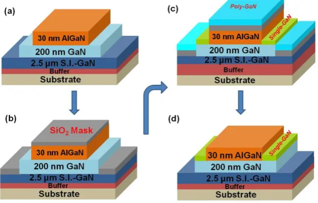
Fig. 1. Schematic illustration of the procedure for selectively regrowing the n+-GaN layers in the source and drain regions by PAMBE.
III.
RESULTS
AND
DISCUSSION
Fig. 2. XRD spectra of the Ti/Al/Ti/Au contacts for (a) the nonalloyed sample and (b) the alloyed sample.
The contact region of the nonalloyed sample was further studied by STEM and AES. From the STEM image in Fig. 3(a), sharp edges between the metals and the regrown GaN layer are observed and no evidence for metal intermixing is found. Fig. 3(b) shows the AES depth profile of Al, Ti, Ga and Au. The result was consistent with the XRD spectra and the STEM profile, which shows that in absence of the annealing process, Ti, Al and Au didn’t have the chance to diffuse after E-beam evaporation. The interface between Ti and n+-GaN is also well defined. Such a flat interface with low defect state density may very well enhance the efficiency and uniformity of current transport, while avoiding the reliability problem mentioned above for the alloyed sample.
Fig. 3. (a) STEM image and (b) AES depth profile of nonalloyed Ti/Al/Ti/Au contact metals on the regrown n+ -GaN layer.
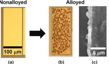
Fig. 4. (a) Optical image of the nonalloyed contact pad, (b) optical image of the alloyed contact pad, and (c) SEM image of the alloyed contact pad showing the lateral diffusion of metals at the pad edge.
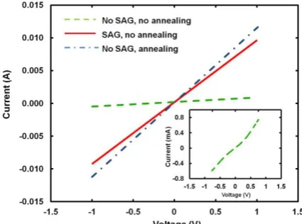
1 V), indicating that Ohmic contact was not achieved in this sample due to the energy barrier at the interface between the nonalloyed metals and GaN epilayer. The regrown GaN layer by PAMBE can effectively narrow the energy barrier to facilitate electron tunneling. As a result, the current transport is significantly enhanced in HEMT-B (I = 9.5 mA at V = 1 V), leading to a linear I-V curve and correspondingly Ohmic behavior. By comparison, the current produced by the alloyed contacts in HEMT-C was 11.5 mA at 1 V. Using the TLM method, the specific contact resistivities for HEMT-B and -C were calculated to be 3.7×10⁻⁵∙cm2 and 1.5×10⁻⁵
∙cm2, respectively. These results demonstrate that nonalloyed HEMT achieved by PAMBE-SAG could exhibit comparable Ohmic contact properties to the conventional alloyed counterpart, while avoiding problems of the latter associated with the high temperature annealing.
Fig. 5. I–V curves of the TLM pattern with 5 µm gap spacing. The inset magnifies the nonlinear I-V curve of HEMT-A.
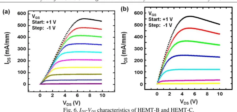
The DC characteristics of HEMT-B and -C were then measured at room temperature. The IDS-VDS
curves were obtained with VDS sweeping from 0 V~10 V, while VGS being biased from 1 V in steps of −1 V until
the devices were pinched off (Fig. 6). The peak drain current of HEMT-B was 555 mA/mm at VGS = 1 V,
comparable to 570 mA/mm of HEMT-C. Moreover, the drain current degradation at VGS= 10 V for HEMT-B is
Fig. 6. IDS-VDS characteristics of HEMT-B and HEMT-C.
Last but not least, the Schottky gate leakage current was measured at the reversed gate bias of -10 V. The leakage currents (Igleak) of HEMT-B and HEMT-C were 3.4 µA and 18.2 µA, respectively. Igleak might be
blocked in the nonalloyed HEMT by the epilayer surface discontinuity resulting from the regrown GaN layers. Besides, since defects generally behave as the electron conduction paths, the elimination of surface defects by the nonalloyed technique might also play an important role in suppressing Igleak.
IV.
CONCLUSION
The nonalloyed technique via PAMBE-SAG is demonstrated as an effective approach to realize low-resistance Ohmic contacts for GaN-based HEMTs. It provides comparable contact properties and current carrying capability, as well as lower gate leakage current than the alloyed counterpart, while avoiding problems of the latter caused by the high temperature annealing process, such as lateral diffusion of contact metals and generation of surface defects. Consequently, PAMBE-SAG facilitates further device downscaling, alleviates defect-induced current degradation, and improves the device reliability and uniformity, therefore is considered promising in fabricating GaN-based nonalloyed HEMTs for high power, high frequency, and high temperature applications.
V.
ACKNOWLEDGEMENTS
This work was supported by Grainger Center for Electric Machinery and Electromechanics of the University of Illinois. The microanalysis was carried out in the Center for Microanalysis of Materials of the University which is partially supported by the U.S. Department of Energy under grant DEF02-91- ER45439.
REFERENCES
[1] N. Tipirneni, A. Koudymov, V. Adivarahan, J. Yang, G. Simin, and M. A. Khan, The 1.6-kV AlGaN/GaN HFETs, IEEE Electron Device Lett. 27(9), 2006, 716-718.
[2] J. W. Chung, J. Lee, E. L. Piner, and T. Palacios, Seamless on-wafer integration of Si(100) MOSFETs and GaN HEMTs”, IEEE Electron Device Lett. 30(10), 2009, 1015-1019.
[3] L. Pang and K. Kim, Bimodal gate-dielectric deposition for improved performance of AlGaN/GaN metal–oxide–semiconductor high-electron-mobility transistors, J. Phys. D: Appl. Phys. 45, 2012, 045105. [4] L. Pang, Y. G. Lian, D. S. Kim, J. H. Lee,and K. Kim, AlGaN/GaN MOSHEMT With High-Quality
Gate–SiO2 Achieved by Room-Temperature Radio Frequency Magnetron Sputtering, IEEE Trans.
Electron Devices, 59(10), 2012, 2650-2655.
[5] D. F. Wang, F. S. Wei, C. Lu, A. Motayed, M. Jah, S. N. Mohammad, K. A. Jones, and L .S. Riba, Low-resistance Ti/Al/Ti/Au multilayer ohmic contact to n-GaN, J. Appl. Phys., 89(11), 2001, 6214-6217. [6] A. Motayed, R. Bathe, R. M. C. Wood, O. S. Diouf, R. D. Vispute, and S. N. Mohammad, Electrical,
thermal, and microstructural characteristics of Ti/Al/Ti/Au multilayer Ohmic contacts to n-type GaN, J. Appl. Phys., 93 (2), 2003, 1087-1094.
[7] Z. F. Fan, S. N. Mohammad, W. Kim, O. Aktas, A. E. Botchkarev, and H. Morkoc, Very low resistance multilayer Ohmic contact to n‐GaN, Appl. Phys. Lett., 68, 1996, 1672-1674.
epitaxial lateral overgrowth of GaN by metalorganic vapor phase epitaxy and hydride vapor phase epitaxy, Mater. Sci. Eng. B, 59, 1999, 104-111.
[15] S. J. Hong and K. Kim, Low-resistance Ohmic contacts for high-power GaN field-effect transistors obtained by selective area growth using plasma-assisted molecular beam epitaxy, Appl. Phys. Lett., 89(4), 2006, 042101.
[16] L. Pang, H. C. Seo, P. Chapman, I. Adesida, and K. Kim, Breakdown Voltage Enhancement of AlGaN/GaN High-Electron-Mobility Transistors via Selective-Area Growth for Ohmic Contacts over Ion Implantation, J. Electron. Mater. 39(5), 2010, 499-503.
[17] H. C. Seo, S. Sivaramakrishnan, J. M. Zuo, L. Pang, P. T. Krein, and K. Kim, Interface analysis of Ti/Al/Ti/Au ohmic contacts with regrown n+‐GaN layers using molecular beam epitaxy, Surf. and Int. Anal., 43(13), 2010, 1627-1631.