IJIRT 148807
INTERNATIONAL JOURNAL OF INNOVATIVE RESEARCH IN TECHNOLOGY159
Design High Speed Low Power Combinational and
Sequential Circuits Using Reversible Decoder
Rajitha Orchu
1, RSVS Aravind
21
Pursuing M.Tech (ES & VLSD), dept. of ECE, Newton’s Institute of Engineering College,
Alugurajupally, Macherla, Guntur dist, AP, India
2
Associate Professor Dept. of ECE, Newton’s Institute of Engineering College, Alugurajupally,
Macherla, Guntur dist, AP, India
Abstract- Reversible logic has presented itself as a prominent technology which plays an imperative role in Quantum Computing. Quantum computing devices theoretically operate at ultra-high speed and consume infinitesimally less power. Research did in this project aims to utilize the idea of reversible logic to break the conventional speed-power trade-off, thereby getting a step closer to realize Quantum computing devices. To authenticate this research, various combinational and sequential circuits are implemented such as N-bit Ripple-carry Adder/subtract or, comparator D-flip flop and ring counter using Reversible gates. The power and speed parameters for the circuits have been indicated, and compared with their conventional non-reversible counterparts. The comparative statistical study proves that circuits employing Reversible logic thus are faster and power efficient.
Index terms- Reversible logic, quantum cost, garbage outputs
I.INTRODUCTION
Reversible rationale is broadly utilized in low power VLSI. Reversible circuits are fit for back-calculation and education in scattered power, as there is no loss of data. Fundamental reversible gates are utilized to accomplish the required usefulness of a reversible circuit. The uniqueness of Reversible rationale is that, there is no loss of data since there is balanced correspondence amongst information sources and yields. This empowers the framework to run in reverse and keeping in mind that doing as such, any middle of the road configuration stage can be altogether inspected. The fan-out of each square in the circuit must be one. This examination paper centers on execution of reversible rationale circuits in which fundamental point is to upgrade speed of the plan. A Reversible adder is outlined utilizing
essential reversible gates. Utilizing this adder, a 8-bit reversible swell convey viper is concocted and afterward contrasted and the traditional 8-bit adder as far as speed, basic ways, equipment utilized. At that point utilizing a similar reversible adder, a Wallace tree multiplier has been executed, and contrasted and the traditional Wallace tree multiplier. With the well-established actuality that successive circuits are the core of computerized outlining, the plan for the control unit of a reversible GCD processor has been proposed utilizing Reversible rationale gates.
II. REVERSIBLE LOGIC
Boolean rationale is said to be reversible if the arrangement of information sources mapped have an equivalent number of yields mapped i.e. they have balanced correspondence. This is acknowledged utilizing reversible gates in the plans. Any circuit having just reversible gates is equipped for disseminating no power. Objectives of Reversible Logic:
A. Quantum Cost: Quantum cost of a circuit is the proportion of execution cost of quantum circuits. All the more preecisely, quantum cost is characterized as the quantity of rudimentary quantum activities expected to understand an gate.
IJIRT 148807
INTERNATIONAL JOURNAL OF INNOVATIVE RESEARCH IN TECHNOLOGY160
C. Garbage Outputs: Garbage yields are those yield signals which don't contribute in driving further squares in the outline. These yields wind up repetitive as they are not required for calculation at a later stage. The trash yields make the framework slower; henceforth for better effectiveness it is important to limit the quantity of waste yields.
D. Feedback: Looping is entirely restricted when planning reversible circuits.
E. Fan-out: The yield of a specific square in the plan can just drive at most one square in the outline. Subsequently it very well may be said that the Fan-out is confined to 1.
III. MAJOR SEVERAL REVERSIBLE LOGIC
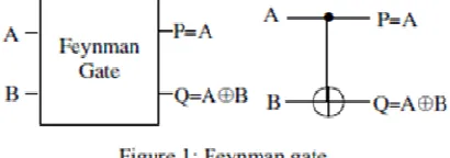
3.1 Feynman Gate It is a 2*2 Feynman gate [13]. The information vector is I (A, B) and the yield vector is O(P, Q). The yields are characterized y P=A, Q=AÅB. Quantum cost of a Feynman gate is 1. Figure 1 demonstrates a 2*2 Feynman gate.
3.2 Double Feynman Gate (F2G)
It is a 3*3 Double Feynman gate [14].The input vector is I (A, B, C) and the yield vector is O (P, Q, R). The yields are characterized by P = A, Q=AÅB, R=AÅC. Quantum cost of twofold Feynman gate is 2. Figure 2 demonstrates a 3*3 Double Feynman gate.
3.3 Toffoli Gate
It is a 3*3 Toffoli gate [6] The info vector is I(A, B, C) and the yield vector is O(P,Q,R). The yields are characterized by P=A, Q=B, R=ABÅC. Quantum cost of a Toffoli gate is 5. Figure 3 demonstrates a 3*3 Toffoli gate.
3.4 Fredkin Gate
It is a 3*3 Fredkin gate [7]. The information vector is I (A, B, C) and the yield vector is O(P, Q, R). The yield is characterized by P=A, Q= A_ BÅAC and R= A_ CÅAB. Quantum cost of a Fredkin gate is 5. Figure 4 demonstrates a 3*3 Fredkin gate.
3.5 Peres Gate
It is a 3*3 Peres gate [15]. The info vector is I (A, B, C) and the yield vector is O (P, Q, R). The yield is characterized by P = A, Q = AÅB and R=ABÅC. Quantum cost of a Peres gate is 4. Figure 5 demonstrates a 3*3 Peres gate.
3.6 Double Peres gate
IJIRT 148807
INTERNATIONAL JOURNAL OF INNOVATIVE RESEARCH IN TECHNOLOGY161
IV. REVERSIBLE N- BIT FULL ADDER/SUBTRACTOR
Figure 7. Reversible Full Adder/Subtractor The Reversible Full Adder/Subtract or Design comprises of two FG, two PG gates, and their interconnections are appeared in the Figure 7. The three information sources are A, B, and Cin, The yields are S/D and C/B. For Ctrl esteem zero the circuit performs addition and Subtraction for Ctrl esteem one. The quantities of Garbage inputs are 1 spoken to by consistent zero. The Garbage yields are 3 spoken to by g1 to g3. The Quantum Cost for the outline is 10. A Quantum Cost preferred standpoint of 11 is gotten when contrasted with Adder/Subtractor utilizing fundamental gates and of 4 when contrasted with Adder/Subtractor utilizing cmos rationale. Quantum Cost advantage is because of the acknowledgment of Arithmetic squares utilizing two PG gates as against two F and one TR gate for Design I and two TR gate.
Figure 8. Reversible N-bit Adder/Subtractor
The tasks of both expansion and subtraction can be performed by a one basic double viper. Such twofold circuit can be outlined by including a faymen gate with each full adder as appeared in underneath figure. The figure above demonstrates the 4 bit parallel twofold viper/subtract or which has two 4 bit contributions as A3A2A1A0 and B3B2B1B0.The mode input control line M is associated with convey contribution of the minimum noteworthy piece of the full adder. This control line chooses the sort of task, regardless of whether expansion or subtraction. At the point when M= 1, the circuit is a subtractor and when M=0, the circuit moves toward becoming adder. The Ex-OR gate comprises of two contributions to which one is associated with the B and other to enter M. At the point when M = 0, B Ex-OR of 0 deliver B. At that point full adders include the B with A with convey input zero and thus an expansion task is performed. At the point when M = 1, B Ex-OR of 0 create B supplement and furthermore convey input is 1. Consequently the supplemented B inputs are added to An and 1 is included through the info convey, only a 2's supplement task. In this manner, the subtraction activity is performed.
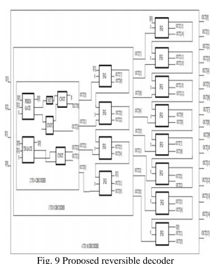
V. PROPOSED REVERSIBLE NUMERICAL DECODER
IJIRT 148807
INTERNATIONAL JOURNAL OF INNOVATIVE RESEARCH IN TECHNOLOGY162
Our proposed 4-bit reversible numerical decoder essentially contains 4 MHNG gate as full adder , and 4 three info MTG and two FG for fan-out and some not gate. It can look at the estimation of two paired numbers An and B by utilizing A-B. We have demonstrated our proposed reversible numerical comparator in Fig.9.
VI. REVERSIBLE D FLIP-FLOP
In this plan reversible edge-activated D Flip-slump is utilized for state advances. Two D-locks are associated in Master-Slave mode to go about as an edge-activated D Flip-tumble. Reversible D-lock is outlined utilizing Feynman and Fredkin gates.
Fig.10 Proposed D Flip-Flop
The D Flip-Flop can be mapped with two FRG and two FG gate. The FRG gate needs D, CLK, 1 and 0 inputs individually in first, second, third and fourth info. The yield D. CLK and D. CLK are acknowledged by one BME in the second and fourth yields. Presently, the second yield D. CLK that is can be utilized as second contribution of one Peres gate.
VII. REVERSIBLE RING COUNTER
Fig.12 Proposed Ring Counter
The fourth yield D. CLK that is R can be utilized as second contribution of another Peres gate. Along these lines, our plan needs just 3 reversible rationale gates with 4 junk yields to outline of D Flip-Flip. The proposed outline of D Flip-Flip is appeared in Figure 10.
SIMULATION RESULTS
Fig.13 Adder/Subtractor
Fig.14 decoder
Fig.15 D Flip-Flop
Fig.16 Ring Counter
IJIRT 148807
INTERNATIONAL JOURNAL OF INNOVATIVE RESEARCH IN TECHNOLOGY163
VIII.CONCLUSION
It can be seen that the performance of digital circuits can be enhanced using reversible gates and have compared N-bit ripple carry reversible adder, Comparators, D Flip-Flop and Ring counter with an irreversible design styles in terms of speed and power; thereby concluding that reversible designs are faster and power efficient. Furthermore, this concept is extended to combinational circuits such as a Wallace tree multiplier using reversible gates, which were simulated and respective results validate prior inferences.
REFERENCES
[1] Landauer, Rolf, "Irreversibility and warmth age in the figuring procedure," IBM Journal of Research and Development , vol.44, no.1.2, pp.261,269, Jan. 2000 doi: 10.1147/rd.441.0261 [2] Bennett, C.H., "Sensible Reversibility of
Computation," IBM Journal of Research and Development , vol.17, no.6, pp.525,532, Nov. 1973 doi: 10.1147/rd.176.0525
[3] B, Raghu Kanth; B, Murali Krishna; G, Phani Kumar; J, Poornima, "A Comparative Study of Reversible Logic Gates", International Journal of VLSI and Signal Processing Applications, vol.2, Issue 1, Feb 2012, (51-55), ISSN 2231-3133 ( Online ).
[4] Morrison, M.; Ranganathan, N., "Outline of a Reversible ALU Based on Novel Programmable Reversible Logic Gate Structures," VLSI (ISVLSI), 2011 IEEE Computer Society Annual Symposium on , vol., no., pp.126,131, 4-6 July 2011 doi: 10.1109/ISVLSI.2011.30.
[5] Nachtigal, M.; Thapliyal, H.; Ranganathan, N., "Plan of a reversible single exactness coasting point multiplier in light of operand decay," Nanotechnology (IEEE-NANO), 2010 tenth IEEE Conference on , vol., no., pp.233,237,
17-20 Aug. 2010 doi:
10.1109/NANO.2010.5697746 (Nachtigal, Thapliyal, and Ranganathan, 2010)
[6] John P. Hayes, "PC Architecture and Organization", McGraw-Hill, 1998. ISBN 10: 0070273553/ISBN 13: 9780070273559
[7] Min-Lun Chuang; Chun-Yao Wang,
"Amalgamation of Reversible Sequential Elements," Design Automation Conference,
2007. ASPDAC '07. Asia and South Pacific , vol., no., pp.420,425, 23-26 Jan. 2007 doi: 10.1109/ASPDAC.2007.358022