IJSRSET1841012 | Received : 02 Oct 2018 | Accepted : 20 Oct 2018 | September-October-2018 [ 4 (10) : 280-289]
Themed Section : Engineering and Technology
280
Design of Non-Volatile Cache Memory Using Spin Orbit Torque MRAM and
Schottky Diode
Venkatesh Ramu1, G N Kodanda Ramaiah2, Santhosh B Panjagal3
1PG GATE Scholar, VLSI System Design, 2Professor & HOD, 3Associate Professor
Electronic & Communication Engineering, Kuppam Engineering College, Kuppam, Andhra Pradesh, India
ABSTRACT
The cache memory design by using Spin Orbit Torque (SOT)-Magnetic (or Magneto-resistive) Random Access Memory (or) MRAM is a next generation developing and promising technology. This SOT-MRAM with schottky diode offers too many benefits such as non-volatility nature, small in size, higher density, low power consumption, scalability and infinite times of endurance. In this project, we provide an exhaustive evaluation of SOT-MRAM with schottky diode at both logic-level and layout-level in terms of size, performance, complexity and energy related parameters and compare them with the existing other cache memory technologies. The designed architecture at layout-level analysis shows that proposed SOT MRAM with schottky diode (using for the L1 & L2-Data-cache and L1& L2-Instruction-cache) will decreases the size by 83.3% and 46.7%, energy consumption reduced by 11.68x and 0.013x and achieve the similar write-read speed compared to an SRAM-only and existing SOT MRAM configuration. Furthermore, the data retention failure chance of proposed SOT-MRAM is 27x lesser than the probability of radiation-induced soft errors in SRAM, for a 90nm technology. All of these benefits will make the SOT-MRAM with schottky diode a viable choice for processor cache memory. Keywords : SOT-spin orbit torque, MRAM- magnetic random access memory, schottky diode, non-volatility, cache memory, reliability, endurance, retention-failure rate.
I.
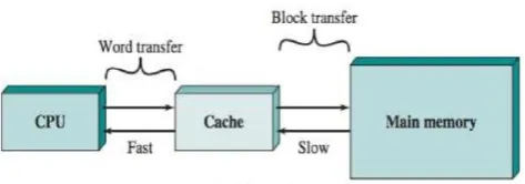
INTRODUCTIONA cache memory is a hardware cache used by the central processing unit (CPU) of a computer to reduce the average time and energy to access data from the main memory RAM. A cache memory is a smaller in size, faster memory and it is closer to the processor core, which stores replicas of the data from frequently used main memory positions. Most of the CPUs have individual independent caches, including data cache and instruction cache, where the data caches are generally organized as a hierarchy of additional cache levels (L1, L2, etc.).
Fig 1.1: Hierarchy of single cache between CPU -main memory.
delivered to the processor for execution because of the reference principle a processor only takes word of data for execution but not a block.
Fig 1.2: Hierarchy of multiple caches between CPU -main memory.
The design of proposed cache memory three-terminal MTJ based on Spin-Orbit Torque (SOT) with schottky diode approach increases the hope of an eventual non-volatile RAM for cache. It represents a new way to achievement over present SRAM, two-terminal MTJ and existing SOT MRAM with read enable MOS transistor limitations by offering high density, reduced power consumption, almost all fully eradicating scaling and read disturb issues.
II.
EXISTING CACHE MEMORIESIn general we have both types of memories volatile and non-volatile and they are suitable for cache and primary memories used based on their speeds. SRAM and DRAM are in volatile category and PCM, Re-RAM, FRAM and emerging ST MRAM are in non-volatile category, all these memories have their own pros and con, as stated in below points.
2.1 SRAM-Static Random Access Memory
The SRAM is a semi-conductor memory that uses bi-stable flip-flop or multi-vibrator to store single bit of data. The SRAM as long as stores the data, but it is volatile nature in the sense that the stored data is lastly lost when the power supply to it is unfenced.
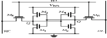
Fig 2.1: A 6T-SRAM bit-cell circuit.
Typically the SRAM cell is consists of six MOS transistors and we also have 4T (due to resistors in pull up stand by power increases), 8T, 10T, or more transistors per bit.The SRAM is the fastest memory with a read-write speed of 1µs, due to many transistors it is highly expensive and low density and till now only used cache memory for storage of frequently usage data in CPU‟s.
2.2 DRAM-Dynamic Random Access Memory
The DRAM stores each data bit in a
particular capacitor with in the integrated circuit. The dynamic, in the sense, it is periodically refreshed for every 1ms time in order to extend the stored data. If these procedures are not done well, a read action can leads to soft errors. Eventually bound keep charge within the Dynamic-RAM can leak via adjacent cells, makes refresh or browse of 1 row ends up in browse disturbance error in associate adjacent or perhaps near row, low speed of 1µs makes it unsuitable for cache memory and usually used as a primary memory.
2.3 Phase Change Memory (PCM)
In the PCM the states of the material crystalline or power in nature defines which type of bit stored. The endurance of the PCM is 109cycles and switching speed is very small and it is ~100 ns. Even though smaller in size, the large switching current requirement for heating to change phase prevents of the PCM bit cell usage for cache memory.
2.4 Resistive RAM (ReRAM)
lower and higher resistive state indicates low and high bit stored respectively. The random behaviour and to several ways between 2 nodes of Re-RAM produces massive variation in shift voltages. Additionally, ReRAM is facing the challenges of low reliability, high resistive variability, and read bit failure issues.
2. 5 Ferroelectric RAM (FRAM)
In the FRAM ferroelectric polarization of electric atoms is used to represent the type of data storage. The channel conductance from drain to source depends on amount of the polarization in ferroelectric material. The issues like depolarization field, gate leakage, and inability to scale the ferroelectric dielectrics limit the further exploration of FRAM.
2.6 Spin Transfer Torque (STT) MRAM
In general the STT-MRAM bit storage identification is based on resistance of the MTJ. The STT-MTJ has higher resistance during out-of-plane and lower resistance during in-plane alignment of the free layer and fixed layers of the MTJ. The STT-MRAM has joint read and write routes, which leads to high write-read latencies and reliability issues. And so, there there's risk of false output read result known as „read disturb‟, also the separate and optimised read-write path is impossible.
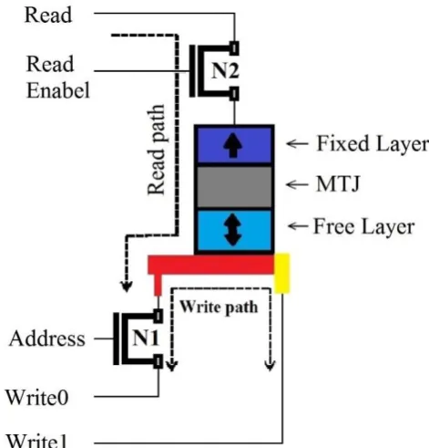
2.7 SOT-MRAM with two access MOS‟s
The SOT devices has independent read and write current paths to solve the very crucial problem of STT-MRAM architecture inherently. Likewise, the SOT-MRAM is very much energy efficient and exhibits faster access, low read-write latencies due to independent read-write path setup. The SOT-MRAM memory delivers data reliable, read-write energy efficient, and fast technology solution, it is ultimately emerged as a strong challenger to replace SRAM in cache. The read enable transistor N2 makes this device large in size and complex routing, so replacing N2 with schottky diode in proposed design.
Fig 2.2: Existing SOT-MRAM read enables NMOS.
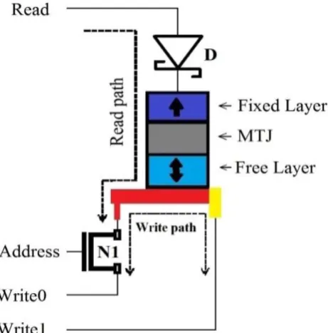
2.9 PROPOSED SOT MRAM WITH SCHOTTKY DIODE
SOT MRAM with schottky diode is used to eliminate the shortcomings of cache memories SRAM and existing SOT MRAM with two access transistors. In this proposed design we use schottky diode D in the place of read enable MOS N2 device and address
access MOS N1 is unchanged. The proposed bit-cell
has an additional terminal with high resistance heavy metal HM2 to separate the read and write paths,
which makes faster access for both operations. The usage of schottky diode reduces the size of bit cell, power and routing complexity compared to existing cache memories. Compared to SRAM the proposed design is more reliable, infinite endurance and 20 years of data retention at 125ºc temperature.
III.
MODULES AND DESCRIPTION3.1 Memory block with transistor
The bit cell array consists of multiple rows and columns of SOT MRAM with one access MOS transistor and one schottky diode for every bit cell. The SOT MRAM used as storing the one bit data, the MOS transistor for accessing the storage cell and schottky diode for preventing write leakage current. The bit cell array of proposed SOT MRAM with one access transistor NMOS N1 and one read through schottky diode D is as shown in the below fig 3.1.
Fig 3.1: Proposed cache SOT-MRAM with schottky diode.
3.1.1 SOT Device Structure
In the SOT-MRAM MTJ device a MgO (MTJ) is sandwiched between distinct character ferromagnetic layers made by CoFeB. In this two ferromagnetic layers one is fixed magnetization, and other one magnetization is freely rotated based on the current feed through the HM1 device. The SOT device is
constructed on the magnetic heavy metal HM1 in
sucha way that bottom layer of free layer lays on magnetic heavy metal HM1 and one end of heavy
metal is connected to high resistance heavy metal HM2. When the write current IW is passed though the
heavy metal HM a strong spin-orbit-interaction (SOI) will take place at the boundary of FL & HM1 and this
effect is due to the Rashba effect and the Spin Hall Effect (SHE). This interaction of FL & HM1 produces
an anti-damping torque and a field-like torque produced due to SHE and Rashba effect respectively. The impact of the induced spin-orbit-interaction is definite by the magnitude of the current IW passing
through the HM1. A write current IW with sufficient
amount of magnitude strength flowing through the HM1 can switch the magnetization of the FL in the
Perpendicular-MTJ SOT-MRAM. Also, the SOI depends on the type of material used in HM1 during
manufacturing, resistivity & dimensions of the HM1,
dimensions of the MTJ, and interface area of the FL/HM1 (WFL, tHM). In the meantime, this SOI is
slightly proportional to the atomic number (Z) of the heavy metal HM1, typically heavy metal HM1 with a
higher atomic number (Z) is superior and they are tungsten (W), platinum (Pt), and tantalum (Ta).
Fig 3.2: Spin Hall effect with Is and IW of MTJ.
The ferromagnetic layer is engaged along the width of HM1 (tHM1) for the proper spin injection Is. A
charge current IW is passed through the HM1which
results in polarization of electrons on the opposite surfaces, this scattering of oppositely spin polarized electrons creates the spin current IS. If we apply the
write charge current IW in the direction-of-x, then
the spin orientation along the direction-of-y makes flow of spin current IS in the direction-of-z which
will produces torque in z-direction. The magnitude of spin current is determined as
Where,
PSHE is spin polarization,
WFM is an area of ferromagnetic layer,
tHM1 is the thickness of HM1,
λSF is spin flip length in Hall metal,
θSHE is spin angle for the HM.
If the area WFM of ferromagnetic layer is greater than
that of HM1, then the IS can be greater than the IW
because of various number of scattering of electrons on the surface so as to generate many units of angular momentum.
3.1.2 SOT-MRAM Write and Read Mechanisms
The SOT-MRAM write operation is as show in the below fig 3.3 a, in which access transistor is activated by making address Add high and giving write current
IW from source line or write line. In this case the
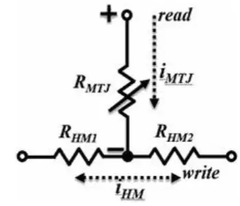
current IW flowing through HM1 alters the magnetic
field orientation due to the SHE. At this time the diode D will be OFF, and limits the leakage current flown outwards and resistances involved are RHM1 &
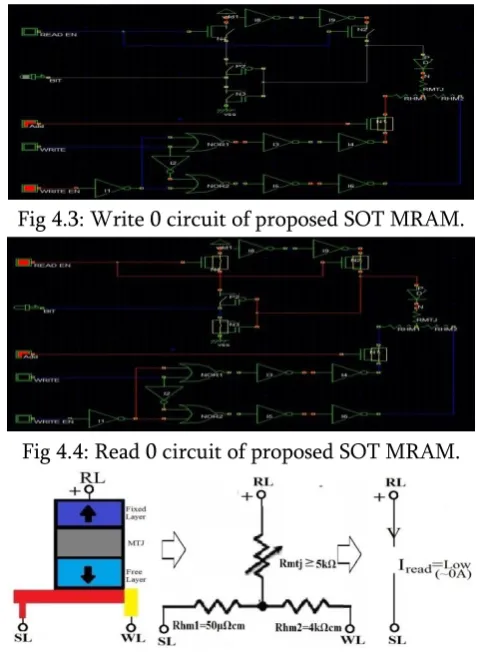
RHM2. Effective write resistance RW= RHM1 + RHM2,
typically RHM1=50–200μΩcm & RHM2 =4kΩcm.
Fig 3.3: SOT-MRAM a) write b) read current directions.
Similarly figure 3.3 b, shows the read mechanism of SOT-MRAM. In this case the read current IR is applied at top and flows through diode and through MTJ and HM1 and grounded at source line if the junction is in-plane or else it would not flow if junction is out-of-plane. In this case the voltage drops will be across diode (0.14-0.2V), RMTJ and RHM1. The
figure 3.4 is the equivalent resistive circuit for SOT-MRAM, in this project we analysed size and power consumption by using this equivalent circuit in the place of SOT MTJ bit cell.
Fig 3.4 SOT-MRAM equivalent resistive network
3.1.2 Schottky diode
The typical arrangement of metal and semiconductor forms a metal-semiconductor junction called as a schottky diode. And this junction is called schottky barrier which leads to very low forward voltage (140mV-200mV) fast and switching speed.
Fig 3.5: Schottky diode schematic.
voltages and heavy reverse leakage current and n-type are comprehensively used.
3.2 Word Line Decoder & Driver
An address decoder in digital logic circuit is a binary decoder circuit that has two or more inputs for address bits and one or plenty variety of outputs for a particular section of the device choice. Whenever the address for a selected device seems at the address inputs, the decoder asserts the choice output for that device. The single decoder will have capacity to serve 2n-types of output devices if it contains n-input address bits. During this project design we tend to use 3-to-8 de-multiplexer, that has three inputs and eight (2^3) output lines. This decoder contains four inputs Read En, address A0, A1 & A2, three inverters I0, I1 & I2, eight 3-input AND gates (AL30-AL37) and eight 2-input AND gates (AL20-AL27), and based on given address A0A1A2 corresponding word line will be activated. The word lines are connected to rows of memory array.
Fig 3.6: Address decoder (3-to-8 demultiplexer).
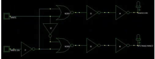
3.3 Write & Driver circuit
A write driver circuit is connected between a bit line and a source line, a switching unit connected between a terminal for supplying a positive Vdd and negative Vss/Gnd voltage sources. Also we have setup to feed this voltage to the heavy metals HM1 & HM2
of the SOT-MRAM bit-cell through access NMOS N1
according to a write enable signal and a write data current flowing through HM1 influence the FL
field state of the magnetic memory cell. The fig 3.7 is the write and driver circuit used in this project and by giving appropriate write & write-en values write 0 and write 1 operation performed.
Fig 3.7: Write and driver circuit setup.
3.4 Sense Amplifier
The sense amplifier generates and sends a reference current through bit-cell from a programmed device NMOS N2 and a non-programmed reference device P2
& N3 is used to read signal from comprising magnetic
tunnel junction (MTJ) cells. The reference current IR is a mid-current which only flows through MTJ when field in free and fixed layer are in-plane (or) during low RMTJ and makes voltage drop across non
programed sense device low and shows read output high and vice-versa.
Fig 3.8: Sensing amplifier circuit.
At the NMOS N2 we will control the amount of current flow to the bit cell only to diode, MTJ and heavy metal HM1, and should not flow through heavy metal HM2 by simply changing the channel length and channel width of NMOS N2. The read current IR, now, is a function of channel width, lengths, gate and source voltages:
IR = µ Cox W/L (Vgs – Vth – Vds/2)2 for VGS ≥ Vth & VDS > VGS – Vth
threshold voltage is changed by varying sio2 thickness or by giving high source to substrate voltages Vsb.
Vt=Vt(0)+(D/€ins€0)√(2€0€siQNVsb) Vsb=0V; Vt(0)=0.2Vdd (=+1Vfor Vdd=5V) Vsb=5V; Vt=0.3Vdd (=+1.5V for Vdd=5V)
IV.
DESIGN & IMPLIMENTATIONThe final design consists of array of SOT MRAM with schottky diodes, address decoders, write & driver circuits and sense amplifier.The design and implimentation of cache memory SOT MRAM with schottky diode is done in “Microwind“ simulator. In this simulator the cache memory design implimentation is done in DSCH “Digital SCHematic editor and simulator“ and Microwind layout.
Fig 4.1: Hierarchy of proposed design.
The fig 4.1 shows the architecture of SOT MRAM with schottky diode, which is present between RAM and processor as a data/instruction cache memory. Similarly below fig shows the 1 bit cell memory write & read architectures of low and high bits respectively.
Fig 4.2: 1 bit Memory with write & read circuit.
Fig 4.3: Write 0 circuit of proposed SOT MRAM.
Fig 4.4: Read 0 circuit of proposed SOT MRAM.
Fig 4.5: SOT MRAM magnetic field, equivalent resistive & current flow during WRITE 0 & READ 0.
WRITE 0: When the write current IW flow from
source line to write line through heavy metal HM1 & HM2 the magnetic field orientation is changed to downwards in free layer due to SHE. The field in fixed layer and free layer is out of plane, which creates high resistance RMTJ (>4KΏ) between two
layers.
READ 0: The high resistance RMTJ leads to no current
flow through MTJ and leads to high voltage across P2 (OFF) & N3 (ON). Now the read output is taken across P2,N3 and N3 (ON) ground appears at bit out which is bit zero.
Fig 4.7: Read 1 circuit of proposed SOT MRAM.
WRITE 1: When the write current Iw flow from write line to source line through heavy metal HM2 &
HM1 the magnetic field orientation is changed to
upwards in free layer due to SHE. The field in fixed layer and free layer is in plane, which creates low resistance between two layers.
Fig 4.8: SOT MRAM magnetic field, equivalent resistive & current flow during WRITE 1 & READ 1.
READ 1: The low resistance RMTJ (50µΏ) leads to
high current flow through MTJ and leads to low voltage across P2 (ON) & N3 (OFF). Now the read output is taken across P2, N3 and P2 (ON) supply appears at bit out which is high bit logic one.
Fig 4.9: 128 bit proposed SOT MRAM with
schottky diode schematic circuit.
The size occupied and power consumption of this
circuit is calculated after generating layout in
microwind by compiling Verilog file. We generate
layout for existing and proposed cache memories
SRAM, existing SOT MRAM with MOS’s and
proposed SOT MRAM with schottky diode.
Fig 4.10: Proposed SOT MRAM with schottky
diode 1-bit cell layout.
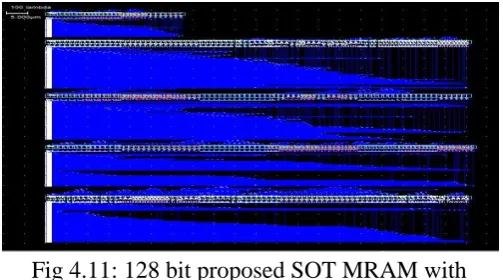
Fig 4.11: 128 bit proposed SOT MRAM with
schottky diode circuit layout.
V.
RESULTS AND COMPARISION
Finally designed layouts for 128 bit memory array for all cache memories SRAM, SOT MRAM with two MOS‟s and proposed SOT MRAM with schottky diode. Also we designed 128 bit full architecture for proposed SOT MRAM with schottky diode. Further post layout we checked the size‟s and power consumptions.
Table 5.1 Size and power comparison. Name &
Parameter
SRAM Existing SOT MRAM
Proposed SOT MRAM
Size
1 Bit cell
79.5µm
2
16.5µm2 8.8µm2
128 Bit cell Array
20424. 4µm2
6895.3 µm2
2908.6 µm2
Power
Write 0 375µW 5.453µW 1.832µW Write 1 365µW 3.733µW 1.829µW Read 0 465µW 8.537µW 2.682µW Read 1 465µW 8.637µW 2.782µW
Mixed 831
µW
72.114 µW
VI.
ADVANTAGES AND APPLICATIONSAdvantages of this SOT-MRAM over existing are Non-volatility in the sense data is not lost if power is interrupted, High speed, due to lower size the density will be very high, Low power consumption, Infinite Endurance and 20 Years data retention.
Applications of this SOT-MRAM include as a cache memory, magnetic field sensor and bio sensor.
VII.
CONCLUSION
For shrinking technologies, non-volatile memories are ultimately promising storage technologies due to their low static power. In this paper, our detailed architecture-level analysis shows that an SOT-only solution and it is the best choice for low power systems. We also found out that for very small memory blocks, such as register files or small L1-caches, SOT-MRAM is still superior to SRAM in terms of area and performance. Compared to an SRAM-only configuration the proposed SOT MRM reduces the area by 88.3%, the energy consumption is improved by 11.68 times and in addition with the same performance. Similarly compared to existing SOT MRAM with read enable MOS configuration the proposed SOT MRAM with schottky diode reduces the area by 46.7%, the energy consumption is improved by 0.013times, reduced routing paths and in addition with the same performance. Furthermore, the data retention failure chance of proposed SOT-MRAM is 27x lesser than the probability of radiation-induced soft errors in SRAM, for a 90nm technology. All of these pluses make SOT-MRAM with schottky diode a viable choice for processor caches.
VIII.
REFERENCES
[1]. F Oboril, R Bishnoi, M Ebrahimi and M B. Tahoor “Evaluation of Hybrid Memory Technologies using SOT-MRAM for On-Chip Cache Hierarchy” Jan 13, 2015.
[2]. M Wang, X Zhao. Y Zhang and W Zhao “Magnetic Tunnel Junction with Perpendicular Anisotropy; Status and Challenges” 10 Aug 2015. [3]. M Imani, Y Kim, A Rahimi, T Rosing “A
Low-Power Hybrid Magnetic Cache Architecture Exploiting Narrow-Width Values” Aug/1/2018. [4]. C Bohac, Manager Applications Engineering,
Everspin Technologies, “Comparing FRAM and MRAM”, Inc. [email protected], 480-347116. # 02130 3/2013.
[5]. M. Imani, et al., "DCC: Double Capacity Cache Architecture for Narrow-Width Values," ACM GLSVLSI, pp. 113-116, 2016.
[6]. Mukherjee, S.; Knut, R.; Mohseni, S.M.; Nguyen, T.A.; Chung, S.; Le, Q.T.; Akerman, J.; Persson, J.; Sahoo, A.; Hazarika, A.; et al. Role of boron diffusion in CoFeB/MgO magnetic tunnel junctions. Phys. Rev. B 2015, 91, 085311.
[7]. J. Tan, et al., "Soft-error reliability and power co-optimization for GPGPUS register file using resistive memory," IEEE DATE, pp. 369-374, 2015.
[8]. Su, L.; Zhao, W.; Zhang, Y.; Querlioz, D.; Zhang, Y.; Klein, J.O.; Dollfus, P.; Bournel, A. Proposal for a graphene-based all-spin logic gate. Appl. Phys. Lett. 2015, 106, 072407.
[9]. S. Li, et al., "Leveraging emerging nonvolatile memory in high-level synthesis with loop transformations," IEEE/ACM ISLPED, pp. 61-66, 2015.
Venkatesh Ramu is PG GATE Scholar, pursuing M.Tech degree in VLSI System Design at the department of ECE in Kuppam Engineering
College, Kuppam affiliated to JNTU Ananthapur. He obtained the B.Tech degree in Electronics and
Communication Engineering from Kuppam
Engineering College, Kuppam affiliated to JNTU Ananthapur. He is doing his M.Tech project on SOT MRAM based cache memory under the guidance of Dr. G N Kodanda Ramaiah & Mr. Santhosh B Panjagal. His areas of interests are Electronics, Analog and Mixed Signal Circuit Design, Memory Design, Digital IC Design and Semiconductor Device Modeling.
Email: [email protected]
Dr. G N Kodanda Ramaiah is a Professor and HOD of Electronics and Communication Engineering in the Kuppam Engineering College,
Kuppam affiliated to JNTU Ananthapur. He obtained the B.E degree in Instrumentation & Technology and M.Tech degree in Bio Medical Instrumentation from Sri J C College of Engineering, Mysore affiliated to Mysore University. He obtained Ph.D. in Signal Processing from JNTU Ananthapur. His areas of interests are Embedded System, IOT, AI, speech processing and signal processing.
Mr. Santhosh B Panjagal is an Associate Professor at the department of Electronics and Communication Engineering in Kuppam Engineering