R E V I E W
Open Access
X-ray generation using carbon nanotubes
Richard J Parmee
*†, Clare M Collins, William I Milne and Matthew T Cole
*†Abstract
Since the discovery of X-rays over a century ago the techniques applied to the engineering of X-ray sources have remained relatively unchanged. From the inception of thermionic electron sources, which, due to simplicity of fabrication, remain central to almost all X-ray applications, there have been few fundamental technological advances. However, with the emergence of ever more demanding medical and inspection techniques, including computed tomography and tomosynthesis, security inspection, high throughput manufacturing and radiotherapy, has resulted in a
considerable level of interest in the development of new fabrication methods. The use of conventional thermionic sources is limited by their slow temporal response and large physical size. In response, field electron emission has emerged as a promising alternative means of deriving a highly controllable electron beam of a well-defined distribution. When coupled to the burgeoning field of nanomaterials, and in particular, carbon nanotubes, such systems present a unique technological opportunity. This review provides a summary of the current state-of-the-art in carbon nanotube-based field emission X-ray sources. We detail the various fabrication techniques and functional advantages associated with their use, including the ability to produce ever smaller electron beam assembles, shaped cathodes, enhanced temporal stability and emergent fast-switching pulsed sources. We conclude with an overview of some of the commercial progress made towards the realisation of an innovative and disruptive technology.
Keywords:X-ray; Field emission; Electron source; Carbon nanotubes; Carbon nanofibres; Nano carbons; Screen printing; Electrophoresis; Vacuum filtration; Chemical vapour deposition; Tomosynthesis; Micro focal
1 Introduction
Since the discovery of X-rays in 1895 [1], X-ray analysis and diagnostics have been some of the most widely researched areas in science and engineering. In the first quarter of the last century, almost half of the Nobel prizes awarded were connected with contributions to this field. Whilst the initial discoveries created great interest towards under-standing the source of this novel light, it was only a short period before the applications of this“new light” became evident. J.J. Thomson had already established their ionising nature [2] and it was recognised that X-rays had different characteristics, initially termed qualitatively as “hard”,
“medium” and “soft” [3]; a classification which related to the relative absorption by soft tissue and bone. Certainly even at this early phase the implications for medical diag-nostics was clear. Early examples included the identification of bullets and bone fractures in wounded soldiers. This resulted in a range of instruments, various densitometers,
chiroscopes and osteoscopes [4]. Soon thereafter this lead to the analysis of the diagnostic capabilities and thera-peutic benefits of this new technology [5]. The increasing importance of X-ray techniques was evident with the de-velopment of X-ray diffraction methods [6-8] which lead ultimately to evidence the structure of DNA [9]. Compton back-scattering and fluorescence provided yet another raft of valuable applications [10-13]. Nevertheless, despite the growing range of X-ray techniques, the primary area of application of X-rays has remained in medical diagnosis. Additionally, X-ray sources have proven important in a wide range of inspection technologies; for medical and analytical, to security and industrial quality control. As illustrated in Figure 1, X-ray sources can be applied to a wide range of applications, including materials analysis (X-ray fluorescence, X-ray diffraction), medical and den-tal diagnosis and treatment (transmission radiography, computed tomography, tomosynthesis, radiotherapy and bracotherapy), electronics inspection, food security, non-destructive testing, thickness and defect monitoring, pharmaceutical quality control, and international border security. Indeed, X-ray sources are ubiquitous and have * Correspondence:[email protected];[email protected]
†Equal contributors
Department of Engineering, Electrical Engineering Division, Cambridge University, Cambridge CB3 0FA, UK
impacted on almost every area and aspect of science and industry.
The strategies for developing new X-ray sources are based on criteria driven by the needs of current applica-tions. Despite the apparent maturity of the technology, many critical challenges remain, including; rapid beam pulsing, dose reduction, improved image contrast, and enhancement of the spatial and temporal resolution. In this review we discuss the use of carbon nanotubes (CNTs) as a platform for emerging novel field emission X-ray sources. We detail the current state-of-the-art in CNT emitter fabrication including the electron source and the gate elec-trode micro-fabrication, functional enhancements including reduced turn-on electric fields and enhanced stability via the incorporation of adlayers, improved X-ray beam distri-bution symmetry achieved through cathode shaping, micro focal sources, pulsed emission, multi-pixel sources, and miniaturisation. We conclude by providing an overview of the commercial progress to date.
2 Review
2.1 Electron emission
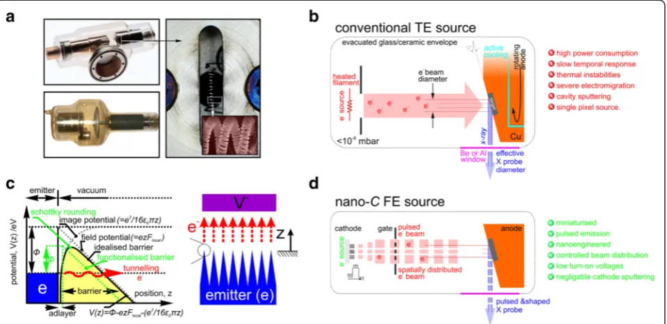
Fundamental to almost all commercial X-ray sources is a source of electrons. Emitted from a cathode, these electrons are directed in a high vacuum towards an anode to which a positive voltage is applied. Emission of electrons will occur from a metal surface when subjected to a high electric field. Figures 2(a) and 2(b) show examples of a commercially available thermionic X-ray sources and their mode of oper-ation, respectively. Figure 2(c) illustrates the approximate band diagram at the metal-vacuum interface. To stimulate appreciable electron emission the electrons must either be excited from the Fermi level over the potential barrier, or
tunnel through the potential barrier. This gives rise to three principle forms of electron emission; photoemission (PE), thermionic emission (TE), and field emission (FE).
PE occurs where the metal is irradiated with an optical source; where the wavelength is selected such that it de-fines an energy greater than the work function (Φ) of the emitter, which typically lies in the ultra violet. As a result, electrons are excited and pass over the potential barrier. PE electron sources have a low efficiency. Much of the in-cident optical radiation is absorbed in the bulk material of the emitter with only a small proportion of the photon population contributing to direct emission. Although PE sources have the potential to achieve extremely fast re-sponse rates, and correspondingly high bandwidths, PE has gained very little traction in most electron emission applications as only very low emission currents are possible. In contrast, TE can derive appreciable current densities that are capable of stimulating X-ray emission. Figure 2(a) shows examples of static and rotating anode TE X-ray sources. Significant current densities, and consequent heat-ing therein, necessitate rotatheat-ing anode and active coolheat-ing systems in TE sources. The core components of these sys-tems are illustrated in Figure 2(b) also outlines the principle mode of operation. Here, sealed in an inexpensive and eas-ily fabricated evacuated glass or ceramic envelope, the elec-trons are liberated from a metallic filament, often made of Tungsten, which is Joule heated to in excess of 1000°C [14]. Since the emission is intimately dependent on the filament temperature [15] – as increasing the emitter temperature allows for much of the electron population to pass over the surface barrier - such tubes enable analogue control over the magnitude of the emission current. In TE sources this beam current is controlled by monitoring the anode current and adjusting the inferred filament temperature using a closed-loop control system. The intrinsic finite ther-mal inertia of the heated coil, when coupled to the lagging response of such feedback control results in a compara-tively slow time response, often several hundreds of milli-seconds. In addition, care must be taken to limit the filament drive current to prevent excessive power dissipation, with subsequent damage or destruction of the filament. Issues with severe electromigration can be a significant challenge. A key design functional parameter is the focal spot size, which is related, in part, to the dimensions of the electron emission area. In the case of TE sources the physical size of the filament, typically of the order of 2 mm in outer diameter and 10 mm in length. This requires the adoption of techniques to provide first order focussing. Some TE X-ray tubes are fitted with two filaments, allowing a choice of focal spot sizes, though this is at the expense of maximum available beam current and hence photon output. In order to achieve further reduction in focal spot size, electrostatic and magnetic focussing techniques are often employed, though at the expense of source complexity and size.
Field emission (FE) offers a number of significant bene-fits. Figure 2(d) illustrates a typical FE source. FE sources are often physically compact compared to their thermi-onic counterparts. The emission process occurs at room temperature and as such does not necessitate a direct heating element. FE is a tunnelling process and provides, as a result, near-instantaneous emission. Pulsed emission with rise times of less than 50μs have been reported [16]. As illustrated above, electrons are emitted under the influ-ence of a high electric field, typically of the order of a few V/μm. These electrons subsequently tunnel through the narrowed potential barrier. Traditionally the emission has been broadly described by Fowler-Nordheim theory [17], although this is now generally considered to be an incom-plete representation in the case of electron emission from most nanomaterials. Nonetheless, a broadly accepted approximation of the field emission current,I, is given by;
I¼ Aβ
2
V2
φ
exp −Bφ
3=2
βV
ð1Þ
whereVis the applied voltage across the vacuum cavity,
φ is the emitter work function, β is the field enhance-ment factor, and A and B are related to physical con-stants [18]. An extended analysis of the background theoretical emission mechanisms can be found in [19]. Various refinements to this model have been applied [20] to take account of the potentially elevated
temperatures during emission and the extreme curvature at the nano emitters apex when whisker-like one dimen-sional nanomaterials are used as the field emission source. Indeed, the high electric field that is required for field emission is closely associated with the curvature and aspect ratio of the emitting material – this field enhancement factor depends upon a number of geomet-rical factors such as the precise form and orientation of the emitter; in general sharp whisker-like tips emit at significantly lower potentials compared to the same ma-terial that has adopted a planar morphology [21]. Such geometry-based arguments are the leading rationale for the use of high aspect ratio nanowires in field emission applications. Contrary to conventional beliefs, studies are emerging which show that the emitter morphology has a much more profound impact on reducing the turn–on and threshold electric fields compared with the effects of the emitter’s work function. However, it remains challen-ging to attain such perturbed, high aspect ratio emitters.
Following early work by Dyke [22,23], in 1968 Spindt published details of a new method of fabricating FE arrays based on Mo conical structures. These structures were 1.5 μm high with a tip radius of 50 nm [24,25]. During the subsequent years, the use of Spindt emitters was widely adopted. They have since become common place in many electron emission systems. Spindts can be found in field emission displays [26-28] to high speed radio frequency devices [18,29,30], such as travelling
wave tubes [31,32]. Extremely high current densities of up to 20 A/cm2 have been achieved [33]. Nevertheless, the issue of developing suitably high current densities with low turn-on voltages has remained an on-going challenge, principally due to demanding requirements on the emit-ting material. At the time, low attainable aspect ratios that Spindt emitters offered, though better than their planar counterparts, limited emitter performance. A new ma-terial capable of forming extremely high aspect ratios was required. Self-assembly via chemical vapour depos-ition and the emergence of nanowires and nanotubes allowed for such high aspect ratios to be fabricated over large areas. The geometry of these new emitters allowed for a corresponding amplification in the field enhancement factor and subsequent reduction in turn-on voltage, typically by an order of magnitude.
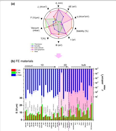
Figure 3(a) summarises the various functional advan-tages of field emission (FE) sources over traditional TE and Schottky sources. The dashed orange circle depicts the characteristics of an ideal electron source. Figure 3(b) illustrates the mean turn-on and threshold electric fields, Eon and Eth respectively, and maximum current density (Jmax) from FE sources fabricated from various materials. Figure 3(b) is structured in order of increasing dimensionality (1D, 2D to 3D/bulk) where each of these dimensional classes is further organised in terms of in-creasing emitter work function (Φ). The mean (±1σ) work functions are shown. Each data point was acquired over multiple studies, nominally three or more, with the figure taking into account material only. The absence ofΦerrors in some of the data indicates that only one such FE study has been conducted, typically due to the recent emergence of the material in question. To extract comparable data all current densities in the considered literature where normalised relative to their maximum current densities, where this normalised value, J’= J/Jmax, where 0≤J’ ≤1. Eonand Ethr were defined as the electric field required to emit 0.1 J’ and 0.3 J’, respectively. For clear assessment purposes of how the material type relates to efficient FE, various emitter morphologies were considered. Note that, on average, there is no clear increase in Jmaxor decrease in Eonor Ethrwith decreasingΦ, as one would expect for a consistent view with earlier band arguments. Indeed, emitter geometry clearly smears out much, if not all of the functional benefits associated with the novel electronic properties of any given material. Nonetheless, the graph-itic carbons are evidently largely unparalleled in their electron emission performance. Combined with the wide range of allotropes observed to date - including the zero-dimensional fullerenes, the one-zero-dimensional nanotubes and nanofibres, the two-dimensional graphenes, and three-dimensional graphite - carbon truly has a morphological character perfectly matched to its impressive electronic properties.
2.2 Field emission application of CNTs
The discovery of carbon nanotubes (CNTs) is generally credited to Iijima in the early 1990s [134], although it is clear that there had been activity in this area for a con-siderable time prior to this [135]. This work, however; lead to a heightened interest which gave rise to some of the first studies on FE using CNTs in 1995 [136,137]. By the start of the following decade a range of applications had been identified to utilise these novel field emitters, including high resolution electron beam microscopes [138-141], flat panel displays [27,28,142-144], RF devices [18,32], electron beam lithography [145-147] and X-ray cathode emitters [148-151]. An early review [146], pro-vides a concise overview of the state-of-the-art prior to 2004. A detailed historical perspective on the develop-ment of CNT-based FE sources is provided in [152]. Here we provide a condensed review of the progress, as it pertains to X-ray sources, since then.
CNTs have some of the highest attainable aspect ratios, high thermal conductivity, low chemical reactivity in non-oxidising atmospheres, highly parallelised en masse fabrication, a low sputtering cross-section, a low secondary electron coefficient, and an insensitivity to direct ion-bombdarment. CNTs are becoming increas-ingly inexpensive with the release of new, ever larger growth reactors. However, field emitters require ultrahigh vacuum (<10−8 mbar) to provide stable operation. This limits their practical application as the material platform on which the emitters are fabricated largely dictates the tip robustness towards poor or compromised vacuum condi-tions which result in aggressive local ionization. In the case of the metallic Spindts, poor vacuum conditions caused tip degradation. As a result, much of the published work has been accomplished using demountable systems, which incorporate vacuum pumps to maintain the performance, although there are some notable exceptions [153,154]. A useful summary on this was published in 2010 [155].
It is the group of applications associated with CNT-based X-ray FE emitters [148] that is the subject of this paper, as the properties of the electron emitting CNTs offer many functional and performance advantages over conventional TE X-ray sources [156,157]. The way in which this review is structured details: shaped cathodes, micro focal sources, pulsed sources, multi-pixel sources, and miniaturised emitters. The review concludes by summarising the commercial progress to date.
Figure 3Comparison of common field emitting materials. (a)Polar plot for the various common-place electron emitters. CNT and graphene based field emitters out-perform such sources across most metrics, where Jmaxthe current density, Eonis the turn-on electric field,‘Vacuum’denotes
the operating vacuum, T the typical operating temperature,Φthe emitter work function,τthe lifetime,‘Stability’is the temporal stability,ηthe electron-optical brightness,ΔE the energy spread of the emitted electrons, dsthe virtual source size. Adapted from [34].(b)Overview of the on and
threshold electric fields (Eonand Ethr, respectively) and maximum current density, Jmax, for various materials used for field emission to date, in order of
dimensionality (1D, 2D and bulk) and increasing work function (Φ), including 1D nanowires - AlQ3[35,36], Si [37-39], MgO [40,41], AlN [42-45], CdS
[46-49], W [50-52], ITO [53], CuPC [54,55], InGaN [56-58], CNTs [59-63] Cu [64-66], ZnO [67-72], GaN [73,74], ZnMgO [70,75], WO [76-79] ), MoO2
[80-82],and ZnS [37,83] -, the 2D platelets - MoS2[84], h-BN [85-88], graphene [89-97], C nanowall [98-100], WS2RGO [101] -, and
vertically aligned forests of CNTs on Co coated W wire, with the electron beam controlled by a counter electrode mounted 0.5 mm from the emitter. This setup produced a beam current of just 1.5 μA, but was sufficient to image onto an X-ray sensitive film a range of samples including integrated circuits. The lifetime of the cathode assembly was little more than one hour and the images exhibited severe noise artefacts. Nevertheless, this work did convin-cingly demonstrate the potential of CNTs in X-ray applications whilst simultaneously highlighting critical functional issues such as fluctuations in emitted beam current that needed to be addressed. Another early example of a functioning X-ray tube was produced by Hagaet al.[150]. Catalytically synthesised CNTs and car-bon nanofibres (CNFs) grown on a Pd wire were used as the FE source, although there was no counter electrode, or gate used to extract the electron beam. This device operated for several hours at 30 kV with a beam current of 50μA. Clear images were acquired, though requiring a long and technologically unacceptable integration time of the order of minutes. The same group produced a triode-configuration (incorporating a gate electrode) which increased the beam current to about 1 mA [151]. Many more examples have now been published on the use of similar triode configurations [149,158-161]. These include designs with additional focusing electrodes for a micro focal imaging system operating at 18 kV, developed utilising 3D beam simulation tools [158].
2.3 Cathode fabrication
All X-ray tubes require the generation of a beam of elec-trons. This electron beam is directed towards the anode,
which subsequently liberates X-rays when impacted. It is the cathode assembly that provides the source of elec-trons and it is the cathode design and materials which dramatically influences the resultant performance. The commercial field of vacuum electronics is now well established and was initially based on Spindt-like emitters, a comprehensive review on which is provided by Temple
et al.[162]. The incorporation of CNTs within the cathode is the focus of this review as it is currently the subject of intense research in an attempt to enhance the electron emission, and hence, X-ray emission performance.
The first FE emitters using one-dimensional carbon al-lotropes were based on CNFs deposited on metallic tips [146,148,150,163]. These sought to enhance the native emission characteristics of the conventional tips by de-positing CNFs, generally by CVD. Subsequent develop-ments, however; centered on the use of planar substrates in attempts to realise more reproducible devices applicable to a wider range of electron emission applications. CNTs may be deposited on the cathode assembly using several different processes [164]. Figure 4 summarises these.
CNT thin films are readily patterned using a variety of techniques. There are numerous aspects which are yet to be well developed in the literature. Nevertheless, the attainable pattern resolution is intimately related to the orientation of the constituent CNTs within the thin film and the patterning technique employed. Aligned CNTs give higher resolution than misaligned CNTs. Wet proc-essed thin films – such as dropped, cast, vacuum fil-trated, sprayed, and screen printed – are fundamentally wet chemistry deposition techniques that can be pat-terned by either post deposition etching or shadow
masking to protect zones from being coated with the CNT inks during the deposition process. These shadow approaches provide a modest maximum resolution of around 100 μm as the inks often bleed beneath the masking layer, resulting in diffuse and uncontrolled edges. Without the application of external driving forces, such as magnetic or electric fields, in such patterns the CNTs are always misaligned with respect to one another. Dip pen nanolithrography and micro-ink jet printing can also be used to drop deposit CNT inks at controlled locations, with a common maximum resolution of 1μm. Nevertheless, again, the CNTs are disordered and misa-ligned. In these additive approaches there remain signifi-cant challenges in preventing the nozzle from clogging during the deposition or the nanolithography tip becom-ing deformed. As a result inkjet printbecom-ing and dip-pen nanolithography necessitates the use of very short CNTs, which dramatically compromises their usefulness in FE applications. Micro-contact printing is another additive approach to cathode patterning. Here a polymeric stamp is inked with a CNT solution and then placed in contact with a substrate which has an engineered surface hydrophobicity to ensure the CNTs adhere. Interfacial engineering marks the broadband application of this technique and often ne-cessitates the use of self-assembled monolayers which act as adhesion promoters. Such approaches have proven use-ful in patterning carbon nanomaterials [165], though their spatial resolution is again limited to a few micrometers at present. In addition to the additive patterning approaches discussed, there are various subtractive means available. Most common is by way of conventional lithographically patterning the deposited CNT thin film, defining a hard mask, and oxygen plasma etching the exposed CNTs. This approach gives high resolution, typically ≤0.4 μm. Never-theless, common to all wet chemistry approaches to CNT deposition remains the fact that the CNTs are disordered and unaligned with respect to one another.
Chemical vapour deposition (CVD) processes dramat-ically bolster the maximum potential resolution to around <0.1 μm by direct patterning of the physical vapour deposited catalyst whilst also allowing for the growth of individual vertically aligned CNTs. Indeed, inclusion of plasma during heating and exposure to the gaseous hydrocarbon and atomic hydrogen sources can be used to assist in the catalytic activity and alignment of the CNTs. CVD is well suited to patterning aligned CNT geometries however it is restrained, at present, to the use of high temperature (>300°C) compatible sub-strates, such as glass, quartz, and Si.
Another important consideration when noting the various merits of the available deposition techniques is the effective roughness and area uniformity achieved. The various deposition techniques produce films of varying thickness uniformity. CVD far exceeds the
degree of uniformity of all other techniques, followed, in rank order, by casting, vacuum filtration, screen printing, and finally spray and drop casting; the latter of which typically gives coffee-stained like thin films that have a significant spatial variation in CNT density. Indeed, CVD, as demonstrated by the group of Milne, has yielded varia-tions in surface roughness of <3% [166]. Nevertheless, for processing simplicity and related cost reductions rather than functional reasons, most CNT-based FE X-ray sources are based on wet chemistry processed thin films. What follows here summarises the fabrication details of some of the more common CNT thin film fabrication techniques, with particular emphasis on those that have been used in CNT-based FE X-ray sources.
2.3.1 Drop, cast and spray
Drop (Figure 4(a)), cast (Figure 4(b)), and spray (Figure 4(c)) approaches have proven, thus far, the fabrication method of choice by many. This is likely a direct conse-quence of their low cost and straightforward processing rather than any direct functional enhancements the fabrication techniques allow for. Drop, cast and spray techniques all require CNT inks. In each case, respect-ively, these are deposited either by direct dropping of the ink, spin coating or casting of the ink, or spray coating of the ink using a pressurised carrier gas. All these approaches initially require wet processing of the as-grown CNTs and it is this which, commonly to all, limits their usefulness and the consequent performance of the resulting X-ray source. The required high power sonication and vacuum unstable surfactants needed to form the stabilised, homogenous inks results in com-promised temporal stability, deleterious hysteresis, and generally degraded emission.
2.3.2 Electrophoresis
annealed at 480°C for 30 min following deposition to mobilise the glass interlayer and reduce the effective interfacial resistance. As with other solution-based fab-rication techniques, in order to reduce the emitters turn-on bias they were taped to activate them; a thresh-old field of 3.5 V/μm was measured (for an emission current density of 10 μA/cm2). Though a simple and low-cost means of defining the pixel size, electrophor-ectially defined emission zones only allow for relatively large cathode diameters, of the order of 2 mm, which reduces the systems functionality. Calderón-Colón et al.
[160] employed photolithography and liquid phase electrophoretic deposition to pattern disordered and unaligned MWCNTs in a homogenous solution with MgCl2 and glass frits. Here the film thickness was broadly controlled by the deposition time and the mag-nitude of the applied voltage, though accurate sample-to-sample reproducibility and control over the thickness, to <10 nm surface roughness, is challenging. Such techniques are comparatively low in uniformity and reproducibility, a direct consequence of the simple macro scale processing. Moreover, the common binder matrices are far from pure, making elucidation of the underlying emission mechanisms somewhat challenging, though nonetheless functional. In-deed, as with all other inking deposition techniques, the emitters do require mechanical activation for the cathodes to be of any practical use, though electrophoretic patterning is indeed rapid and simple to implement.
2.3.3 Vacuum filtration & screen printing
Many of the FE X-ray sources demonstrated have employed screen printed or vacuum filtrated CNT thin films [156,169-171] (Figure 4(d)). Here CNT solutions are deposited at the macro-scale and form highly disor-dered, nominally planar, spaghetti-like networks with but a few individual CNTs standing upright, at many un-registered angles relative to one another. In the case of vacuum filtration the CNT ink is poured onto a porous mixed (nitro) cellulose ester membrane, which has a par-tial vacuum applied on its opposite side. Such porous membranes have controlled apertures, typically around 0.2μm in diameter. The reduced pressure stimulates the solvent within the CNT ink to pass through the mem-brane, whilst the membrane stops the CNTs from pass-ing. Once the ink reservoir is depleted the thin film is rinsed with de-ionised water to remove much of the deleterious surfactants, leaving a thin CNT film on the membrane. Note, however; that much of the surfactant still remains even after extensive rinsing using deionised water. The CNT thin film can then be transferred to an arbitrary acetone-resistant substrate by applying modest pressure (40 g/cm2) and heat (ca. 70°C) for an extended period of time (often of the order of 3 h). The mem-brane is then dissolved, by exposure to acetone or
methanol, and the CNT thin film remains. The CNT film thickness, and hence sheet resistance and optical transparency, is controlled by adjusting the amount of CNT ink filtered through the membrane.
CNT thin film fabrication by vacuum filtration has been employed for more than a decade. It offers a rapid, low cost way to fabricate CNT thin films. Little to no infrastructure is required and the films can be processed rapidly, over large areas. Nonetheless, as in the case of drop, cast and spray, suchchemi doucheprocessing re-quires stabilised inks. CNTs experience high inter-tube van der Waals forces; they tend to agglomerate. Though this interaction has been exploited elsewhere to fabricate novel aligned nanostructured membranes [172], such agglomeration is problematic in producing homogenous CNT inks and solutions. As such, various, often sodium-based, surfactants such as sodium dode-cylbenzene sulphate, sodium dodecyl sulphate, and Tri-ton X are required to produce homogenous solutions with the CNTs well-dispersed throughout the solution. Further aggressive acid treatments and extended dura-tions under high power ultrasonication significantly de-grade the length, crystallinity and subsequent electronic character of the CNTs which necessarily limits the elec-tron emission performance. These inks are then trans-ferred to metallic disks using conventional screen printing methods or vacuum coated mixed cellulose ester mem-branes that are subsequently dissolved in acetone follow-ing transfer [173]. The morphology of these films is highly disordered. They typically lack high aspect ratio protru-sions, resulting in poor field emission performance. FEs fabricated in this way have a number of intrinsic problems; chiefly that mechanical taping is required to activate the surfaces and enhance their field emission characteristics. Taping, using adhesive coated tape, increases the surface roughness of the CNT thin-films. It is a macro-scale process and affords very little reproducibility, Moreover; the necessary surfactants are usually vacuum unstable giving rise to emission profiles that deleteriously drift with time [170,174-176]. CNT inks can often have significant out-gassing [177] when even modestly heated, comprom-ising the vacuum envelope. The resultant reduction in field emission performance and reduced current density has, as a result, prevented CNT-based pastes and ink from gaining commercial traction, though cathodes fabricated in this way appeal as the reduced reproducibility is off-set by the ease of fabrication. Such films are also somewhat dynamic and often have weak adhesion to the substrate. Their morphology shifts with time during the application of a high electric field due to the intrinsic torque induc-tion within the CNTs due to the tip or root posiinduc-tioning of the growth catalyst particle.
screen printing, as illustrated in Figure 4(e), employed ball-milled pastes combined with inorganic fillers includ-ing Ag and Ni alloyed nano-particles and oxides in an ethyl cellulose powder and terpineol solvent. No surfac-tants were used. The pastes were deposited on indium tin oxide coated glass substrates followed by 300°C post-bake to remove residual solvents. The derived slurry showed strong adhesion to the substrate, good uniform-ity and reproducibiluniform-ity with a current densuniform-ity of up to 350 mA/cm2. Nevertheless, ball-milling degrades the graphitic quality of the MWCNTs, which adversely impacts the long-term time stability relative to high quality crystalline material, although these devices did show excellent high-temperature operation (up to 800°C), robustness towards harsh vacuum environments, impres-sive spatial uniformity, a low turn on voltage of 1 V/μm, and enhanced temporal stability relative to conventional CNT pastes, although the anode current was still de-graded by around 30% under DC operation over a 100 hr test period. Another fabrication problem associated with screen printing is the limitation on the pattern resolution. The sonicated CNTs within the inks are typically of the order of 5μm in length. These can clog the screen print-ing mesh resultprint-ing in a low porosity and inability to print.
Formation of stabilised, homogenous inks is central to drop, cast, spray, vacuum filtration and screen printing. The formation of these inks, as highlighted above, requires deleterious ultra-sonication and aggressive acid treatments, both of which degrade the length and elec-tronic character of the CNTs. Though the necessary wet chemistry approaches provide a facile, rapid and inex-pensive route to fabricate the emitter, the constituent CNTs are coated with deleterious vacuum unstable surfactants that can only be removed following high temperature post-deposition treatments which, if not fully removed, would otherwise cause significant out-gassing during FE operation [160]. Maintaining slurry and ink consistency over time and between batches is difficult, which manifests as a reduction in device-to-device reproducibility. It is also challenging to pattern emitters fabricated in this way though screen printing (the migration of CNT inks through patterned apertures within a regular mesh), as demonstrated by Kim et al.
Though screen printing is indeed large-area compatible, it is rather low resolution and thus limits the degree of control over the detailed design of the electron source. Oxygen plasma etching coupled to conventional litho-graphic techniques is another viable option though significant surface roughness of the CNT thin film can again compromise the maximum resolution. Moreover, plasma etching techniques are only applicable to non-organic substrates.
While there have been reports that electrophoresis can produce a degree of alignment [179,180] this is relative
only to very randomly orientated screen printing and ink-based processes. Misalignment prevents any fabri-cated devices from realising the full field enhancement factor of the composite CNTs; in order to achieve this al-ternative fabrication methods capable of aligning,en masse, the CNTs must be considered, with chemical vapour deposition being the most promising method to date.
2.3.4 Chemical vapour deposition
Chemical vapour deposition (CVD) (Figure 4(f )) pro-vides a more controllable means of growing CNTs. The CNTs self-assemble from atomic units in a highly paral-lelised process, which when coupled with high resolution lithographic techniques to pattern the catalyst material, allows for near nano-scale engineering of the CNTs and CNFs. CVD techniques mediate the growth of chem-ically untreated disordered or aligned CNT thin films depending on the substrate, catalyst and growth precur-sors employed. In a typical implementation, Silicon is coated with a physical vapour deposited metal catalyst which is then patterned via lithographic or masking techniques by either additive or subtractive process, such as magnetron sputtering, or plasma etching, respectively. The substrate is then heated to temperatures often in excess of 500°C, and the growth of the CNTs on these sites is initiated by supplying a hydrocarbon feedstock gas, such as CH4 or C2H2, combined with an a-C etching gas species, typically H2 or NH3both of which readily pyrolyse to give a constant supply of carbon and atomic hydrogen. In situ plasma can also be employed to enhance the catalysis and align the CNTs during growth. Coleet al.have compiled a concise overview of the CVD of nanocarbons, available elsewhere [181].
characteristics. Though film reorganisation benefits the long term stability, in that degraded CNTs are in essence replaced, the short term temporal stability is likely to be very poor. More than 100 cathodes were tested and a poor reproducibility was indeed noted, a probable consequence of the disorder and uncontrolled microscale morphology of the emitter.
As is the case for the screen printed and vacuum filtra-tion methods, one potential problem is the degree of ad-hesion between the CNT and the substrate when exposed to high electric fields. Detailed control of the underlying catalysis has shown that such emitter removal concerns can be solved. Li and Coleet al.showed very low variation in anode current of < ±0.7% for constant emission over >200 hrs using an ITO/Ni (10/1 nm) bilayer catalyst which effectively enhanced the degree of adhesion [183].
Using rapid thermal CVD, Kim et al. [184] deposited CNTs directly on stainless steel sheets coated with TiN/ Ni. The emitters showed a maximum current of 2 mA (data on the emitter area was unavailable) at an anode potential of 5 kV. The CNTs were 30μm long, with Ra-man analysis suggesting a very defective material, whilst scanning electron microscopy showed vertically aligned forests with a high packing density. Though the emission showed good performance the geometry was not opti-mised; the dense forest results in significant shielding of the CNTs from the applied electric field – the material appears as bulk - such that the full field enhancement factor of the CNTs was not realised in this instance. Whilst individual, one dimensional nanowire and nano-tube emitters have been empirically evidenced to pro-duce the highest electric fields, the proximity of other emitters will effectively shield the field enhancement [146,185]. In a field emission device, where our interest is in the total available current density, the optimum arrangement will not be that with the highest density of emitters [186,187]. In addition, if the emission pattern of the field emitter is not uniform CVD growth can result in individual CNTs, or structures such as CNT pillar ar-rays and toroids [160,167,188-191]. Patterns of control electrodes may be grown, in such a way as to focus or concentrate the field from the tip.
The use of CVD to nanoengineer X-ray sources has remained in its infancy due to a number of challenges in explicating the underlying material growth. Nevertheless, following recent advances in the understanding of nano-carbon catalysis [192-194], the use of CVD-grown CNTs and CNFs in FE X-ray sources appears to be accelerating with it emerging as an emerging as an exciting candidate for viable commercialisation.
2.4 Diode & triode configurations
The first examples of X-ray emitters using FE electron sources employed diode configurations which comprised
only of a cathode and an anode. However, in such devices the emission current was a function only of the anode voltage. As a result such diode configurations gave rather limited control over the magnitude of the emission current for most applications. To more accur-ately control the emission current, whilst also providing a degree of protection, it is now standard procedure to introduce a third electrode. This gate electrode gives rise to a triode configuration. Early in the development of CNT-based FE X-ray sources, Sugie et al. [148] intro-duced a counter-electrode wire. Since this naturally produced an anisotropic beam, the control mechanism of choice became a perforated grid, or gate electrode. The purpose of the gate is to create a local electric field that draws the electrons away from the principal emis-sion beam. However, in practice a significant proportion of the emitted electrons will be attracted towards the gate electrode. The gate must therefore be sufficiently transparent to allow the maximum number of electrons to pass to the anode. It is normal that >50% of the cathode current is directed to the gate, thereby limiting the efficiency of such devices. However, there has been recent interesting work on improving the transparency of the gate by incorporating graphene layers. This has shown a substantial improvement in efficiency to around 60% [195] though the technique has yet to be applied to X-ray sources.
Further, the addition of a fourth electrode, mounted just above the gate, has been described [154]. This elec-trode had many apertures for each gate perforation, and was mounted approximately 0.2 mm above the gate elec-trode. The claimed transmittance of the CNT cathode electrons, to the anode was up to 80%. In addition, there are numerous examples of the addition of a further electrostatic focusing electrodes used to reduce the focal spot size. This is described in more detail below.
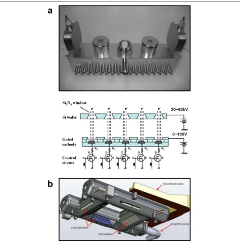
2.5 Demountable tubes
based sources have been fabricated in what are largely deemed demountable tubes. Clearly, the nature of devices developed for research and design iteration, this is the sensible choice. However some improvements – for example, miniaturisation–have seen the development of a sealed construction [150,154,197,198].
2.6 Functional enhancements
Table 1 below summarises the cumulative literature to-date on the progress towards the realisation of a functionally enhanced CNT-based FE X-ray source. Italicised values indicate the highest achieved stan-dards at the time of publication. What follows is a de-tailed overview and assessment of some of the leading studies with regards to their functional enhancements, fabrication methods, and emission performance.
2.6.1 Beam profiling
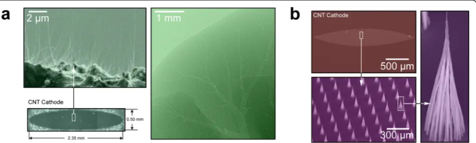
Many groups have grown CNTs, by CVD or derivatives thereof, directly on conical or other shaped tips, on common Spindt-like materials [213], Si [169,205,214] or bulk metals [200]. As such, these systems do not exploit the full geometric potential of the CNTs; they simply amplify, often only marginally, the existing field en-hancement factor of the tip structures and almost always result in an induced asymmetry in the electron beam profile that is challenging to accommodate with conven-tional electrostatic focussing. Indeed, even convenconven-tional X-ray TE cathode assemblies will, in general, produce an anisotropic focal spot, as a result of the electron beam dimensions, imperfect focusing, and the impact of the target angle. One potential route to realising symmet-rical X-ray sources with shaped beam profiles is to shape the cathode such that the emergent electron beam defines, at least in part, the spatial distribution of the emergent X-ray beam. This requires patterning of indi-vidual CNTs or CNT forests into well-defined geom-etries. Several groups have considered the use of cathode shaping as a mean to achieve beam profiling. Most have used elliptical cathode geometries to define a circular distribution of the emergent X-ray beam [160]. Two examples are as shown in Figure 5(a,b). Shaping has also been shown to enhance the FE performance by exploit-ing the natively high field enhancement factor at the shaped emitter’s edges. In particular, the group of Milne have shown field emission properties of individual CNFs and patterned forests [185,215,216]. No systematic studies on the effect of shaped cathode eccentricity, or other controlled geometrical parameter, on the symmetry or profiling of the emergent X-ray beam appear to have been considered to date. Indeed, the electrophoretically depos-ited and photolithographically patterned elliptical cath-odes of Calderón-Colón et al. [160] showed impressive emission characteristics though no detailed assessment of
the emergent beam shape was reported, making is difficult to assess the success of such beam shaping techniques (Figure 5a).
Using Si-supported CNT arrays, Ryu et al. demon-strated the potential of CVD in X-ray source applica-tions [205]. A resist-assisted patterning process was used to produce a cathode assembly consisting of a gate and focusing electrode. This assembly was approximately 0.5 mm × 2.0 mm and gave an isotropic focal spot [205]. Ryuet al.also described a further shaping technique for post processing the as-grown vertically aligned CNTs. Here they used hydrofluoric acid to produce an array of conical pillars (Figure 5b), rather reminiscent of earlier Spindt emitters. Hydrofluoric acid, though cheap and readily available, is rather hazardous to handle and poses a significant health risk. This somewhat limits the com-mercial viability of the compaction technique presented. Nevertheless, they demonstrated anode currents of up to 90 mA at 7.8 V/μm, with a turn-on electric field of ap-proximately 3 V/μm. To increase the geometric uni-formity of the emitters the team used an electrical aging treatment, which degrades the taller tubes and bundles that would dominate the emission. For a high perform-ing emitter this agperform-ing, also termed seasonperform-ing, is not de-sirable and CNTs of very uniform height and diameter are preferred, as evidenced by Teoet al.[166], to obviate the need for such post-growth treatments. Nevertheless, part of the Ryuet al.ageing process [205] was to remove the Ni catalyst particles at the CNTs apex, which they argued reduced the emission current. Detailed analysis and theoretical studies surmising the emission implica-tions of the metallic nanoparticle in the emitter tip are lacking in the literature.
2.6.2 High beam current
[159] 2005 Electrophoresis 10 mA (15 V/μm) 40 DC <5% ~2.6 (/) 0.15 Micro focus
[199] 2007 PE-CVD (W and Pd wire) 50μA ~ (3 V/μA) 15 DC / / 0.05 Micro focus
[163] 2007 PE-CVD (W wire) 26μA (5 V/μm) 40 DC / 1.6 (10 mA/cm2) 0.005 Micro focus
[200] 2010 PE-CVD (W and Pd wire) 0.1 mA (/) 25 DC <15% 3.2 (/) 0.0004 Micro focus
[201] 2004 Solution Processed 6 mA (15 V/μm) 60 107–8 <±1% ~7.1 (/) 0.15 × 0.03 Micro focus high
pulse rate
[149] 2002 Electrophoresis 28 mA (/) 14 103 ±2-4% 2.0 (1 mA/cm2) 3.2 Pulsed
[202] 2006 / 1 mA (/) 40 1 ~50% / 0.2 Pulsed multi-pixel
[203] 2009 Electrophoretic 18 mA 30 102 / ~5.0 (/) 0.5 × 0.3 Pulsed multi-pixel
(25×1)
[171] 2011 Screen Printing 43 mA (/) 45 5 ±0.2% / 0.6 Pulsed multi-pixel
(31×1)
[203] 2009 Electrophoresis 18 mA (/) 40 103 <7% 6.5 (/) 0.1 Multi-pixel (25×1)
shaped cathode
[169] 2011 Electrophoresis 3.5 mA (7.5 V/μm) 1.4 DC / 3.5 (10μA/cm2) 2.0 Multi-pixel (5×10)
[204] 2013 CVD 0.6 mA (16 V/μm) 40 DC / ~8 (/) / Ballasted
[160] 2009 Electrophoresis 7.0 mA (8.5 V/μm) 50 10 ±13% 5 (/) 0.1 Shaped cathode
[205] 2012 CVD 90 mA(7.5 V/μm) 50 DC / 3.0 (0.1 mA) / Shaped cathode
[206] 2006 DC Electrophoresis 150 mA (12 V/μm) 40 102 / / 0.03 Shaped cathode
pulsed micro focus
[182] 2004 CVD (Mo disk) ca. 15 mA (4.6 V/μm) 1.1 10−1 / ~2.0 (/) 0.5 Miniature battery
operated
[150] 2004 CVD 0.3 mA (7.0 V/μm) 30 DC ±8% / / Miniature
[198] 2005 / ~40μA (/) / 2x10³ ~50% / 1.0 Miniature
[207] 2012 Paste 0.6 mA (1.4 V/μm) 70 DC ±2% / 3.7 Miniature
[208] 2013 Paste 1.2 mA (4.7 V/μm) 25 10 ~ <1% ~3.5 (/) / Miniature
[209] 2004 CVD (Mo disk) ~2 mA (4.65 V/μm) 10 10−1 / 2.2 (10 nA) 0.5 Miniature pulsed
[210] 2006 Ion bombardment (polyimide) / 25 6x10² / 1.5 (1μA/cm2) / /
[148] 2001 CVD (metal wire) 1.5μA (20 V/μm) 60 DC ±10% / / /
[151] 2004 PE-CVD (W and Pd wire) 1 mA (/) 40 DC ±8% / 2.0 /
[184] 2007 CVD 2.0 mA (0.5 V/μm) 10 DC ~50% ~0.2(/) / /
[211] 2008 PE-CVD (Pd wire) 1.0 mA (/) 50 DC ±10% / 3.0 /
[154,212] 2014 Screen Printing 15 mA (2.6 V/μm) 20 10 / / 0.3 /
Ia: Anode current (A);
Ja: Anode current density (A/cm2); / denotes values not given.
Nano
Convergenc
e
(2015) 2:1
Page
12
of
corresponding to 5×10⁶ A/cm2 [218], which is signifi-cantly larger than any attained by Spindt-like emitters fabricated to date.
Using electrophoretically deposited SWCNTs [167], high electron beam currents have been achieved using a triode configuration by Yue et al. [149]. Here, the gate assembly was mounted approximately 100 μm adjacent to the CNT electron emitter resulting in a device geom-etry capable of sustaining a beam current of several milliamps, although this would likely prove challenging to manufacture in a practical X-ray source. In addition, they demonstrated peak pulse currents of up to 28 mA (emitted area not stipulated), without vacuum breakdown, at an anode potential of 14 kV. Using CVD grown CNT arrays, Ryu et al. [205] reported emission currents of up to 90 mA (emitted area not stipulated) in a diode config-uration, although in a gate-controlled triode arrangement, the beam currents were substantially reduced.
Some improvement towards increasing the current density has also been achieved by controlling the emitter morphology. Toroidal CNT arrays, which have a central void [191], are one such example. By subsequent surface treatments, it is also possible to enhance the native FE characteristics of such arrays by means of the formation of nano tips, tepees and micro cones, as outlined previously [190,205]. The use of emitter forming post-treatments has also been widely investigated. One leading example is the use of conical CNTs which enhanced the beam current and stabilised the emitter geometry. Another alternative to-wards higher beam currents is to augment the electronic character of the CNTs, via the dry or wet deposition of various adlayers. Such adlayers adjust the interfacial charac-teristics at the critical emitter-vacuum interface. This often leads to a decrease in the turn-on voltage and increase the emission current density at a given anode bias. As was highlighted above, FE is highly surface sensitive; at
107 A/cm2 a 1% change in the surface work function, due to intentional adlayer sputtering or indirect sput-tering from reactive gas species in the vacuum cavity, can increase the current density by more than 10% [152]. Little work has been reported on the use of adlayers to enhance the emission performance of CNT-based FE X-ray sources. Nevertheless, significant advantages may be achieved by carefully designing the emitter-vacuum interface to provide high emission cur-rents, limit adverse effects of vacuum leakage, prevent unintentional work function shifts, as well as robust-ness towards local ionisation and plasma etching, all of which are critical in ensuring long term stability.
2.6.3 Enhanced temporal stability
The failure mechanisms of Spindt and CNT based emit-ters, which are similar in many respects, have been widely studied [219], most notably by Bonardet al.[220]. Ther-mal migration, field sharpening and subsequent avalanche breakdown are perhaps the most common failure mech-anism in such whisker-like emission geometries [221]. Although recent work on CNT-based emitters has shown impressive lifetimes of 7000 hours, with only a 10% emis-sion degradation [222], it remains an on-going challenge to design and fabricate high temporally stable emitters. As noted previously, the electron emission is sensitive to the bulk emitting material and the emitters’surface chemistry. CNTs have a high sublimation temperature and high max-imum current densities, making them resilient towards arcing events. Pristine CNTs are also largely inert, al-though when defects are added to the graphitic lattice, often through plasma processing, they are readily dam-aged and the formed dangling bonds bolster the CNTs emission performance, though often at the expense of the long term stability. The enhanced emission is due to the augmented surface characteristics. This effect is often
noted as a shift to higher turn-on bias during hysteresis studies. Indeed, many plasma and some dopants, such as oxygen when the emitter outgases, can be particularly damaging to the CNTs. Local Ohmic (I2R) heating can also increase the rate of emitter degradation, as can vacuum breakdown. It has been shown that the axial resistance of CNFs increases with increasing temperature. Interestingly this intrinsic property helps protect the CNFs from degradation during local heating and helps prevent thermal run-away deleteriously increasing the emission current [221]. Vacuum breakdown results in the emission of extremely high current densities which may cause a plausible local oxygen micro-plasma formation – this etches the CNTs, particularly at their apex. This shaping stimulates the formation of defects in the graphitic lattice, which preferentially emit electrons, thereby enhancing the emission, however; this results in a temporally unstable emission profile. The CNTs can be sharpened with time, which tends to increase the emission current, or can alter-natively be entirely ablated, which reduces the emission current due to the reduced number of electron emitters available.
There have been various methodologies proposed which attempt to reduce temporal instabilities. Thermal annealing or electrostatic seasoning, to remove residual surfactants and non-uniform emitter profiles, are per-haps the most common and certainly the most simple and readily implemented [160]. During thermal anneal-ing the cathode assemblies are heated to temperatures in excess of 300°C under high vacuum conditions. This out-gases the emitter, removing weakly surface bound chemisobed species. This increases the work function uniformity across the surface of the emitter. Such out-gassing techniques are also useful in emitter recovery following an arcing event. Arcing events stimulate high current flow which heats and subsequently out-gases the emitter. This out-gassing can lead to further transient arcs which, if allowed to continue, will degrade the emit-ter. If the emitter is initially well out-gassed any local arcs will only marginally increase the cavity pressure and the emitter will stabilise more rapidly. Annealing is also employed to enhance the pressure of the vacuum cavity, making local plasma formation increasingly unlikely. In the case of electrostatic seasoning, the extraction electric field is slowly ramped up to around 80% of the nominal emission voltage. The emitters are then left emitting for tens to hundreds of hours to increase the surface smoothness of the emitter and hence, stabilise the emis-sion current. Such approaches are critical in achieving intrinsic emitter stability, and though feedback tech-niques have been employed to artificially control the stability, engineering intrinsic stability remains central to the formation of a long-term stable emitter. In feedback based systems, in the same way as conventional TE
generator designs, the anode current is monitored and the extraction voltage adjusted accordingly to maintain a known, safe, emission current. Though a viable and widely adopted approach to ensuring emitter stability, the slow response times of the feedback loop cannot entirely remove transient effects, such as arcing events, and only careful design of the electron source can facili-tate this.
Though CVD is certainly coming to the fore as the most reproducible fabrication technique with the finest degree of control over the emitter design, it, like other techniques, is faced with issues of tip-to-tip uniformity. Poor uniformity in effective surface roughness is known to de-stabilise the temporal stability. Indeed, wet chem-istry ink approaches to emitter fabrication result in much greater surface roughness, and this exacerbates and further compromises their temporal stability. Small height variations between tips can instigate preferential emission from a small proportion of the longer CNTs, which consequently burn-out. It has been shown else-where that individual CNTs can in practice pass a current of several microamps [223]. Currents in excess of this threshold cause the CNT to sublime, which man-ifests as a temporal instability in the anode current, and subsequent X-ray emission. In the case of CVD-synthesised CNT emitters one solution – originally de-scribed for application with Spindt emitters [224] and initially proposed for general electron emission applica-tions by [183]–consisted of integrating a ballast resistor micro-fabricated in series with the electron emitter. Here resistive deposited layers are fabricated in series with the electron emitters. The series resistance ballasts the emission, functioning as a current limiting resist-ance, preventing emitter sublimation, subsequently enhancing temporal stability. Yet to be applied immedi-ately to the design of an X-ray source, the group of Milne have developed a novel field effect transistor (FET) ballasted field emission source, where each indi-vidual CNF electron source is equipped with its own dedicated FET ballast layer which is capable of limiting, and electronically controlling, the emission current to prevent emitter sublimation and significant temporal instabilities [183]. Other thin film deposition techniques have also been considered [204,225] though these too have yet to gain any significant interest.
incorporated. Several approaches have been taken to improve the robustness of the emitting elements by in-creasing the degree of adhesion between the CNTs and the supporting substrate. Bundles of vertically aligned CNTs - typically with a height of around 10 μm or less, and a diameter of 30 μm, have been shown to be one such robust assembly, that is not readily damaged or easily removed. However, FE preferentially occurs at the periphery of the patterned CNT forest or array [188,189] suggesting that if some CNTs are in fact removed the emission stability may simply be recovered by new CNTs contributing the emission current of those removed; emitter areal design can in part accommodate and en-gineer out temporal instabilities. Nevertheless, there is a continuing effort to engineer the CNT-support interface to enhance the degree of adhesion and hence enhance the temporal stability. In the case of ink approaches various solution additives have been exploited, such as glass frits [160], though the exact implications of such approaches with regards to the turn-on field and max-imum current density remain unclear.
Elsewhere there has been significant work on the use of surface treatments to stabilise the temporal stability of the electron emission [205,226]. As discussed previ-ously, such low work function adlayers do indeed in-crease the emission current density, though they also, depending on the adlayer material and means of depos-ition, hermetically seal the CNTs – which act as a high aspect support structure – thereby increasing the emit-ters stability [225].
2.6.4 Micro focal sources
FE sources have the potential for extremely high spatial modulation. By controlling, the electron emitter location at the nanoscale, coarse control over the position of the electron beam, and subsequent X-ray beam are possible. A range of focussing techniques has also been developed to reduce the electron beam focal spot size. Standard X-ray tubes have a focal spot size of typically around 1 mm diameter. For greater spatial resolution, “mini-focus” X-ray tubes have been developed, with a spot size down to 50μm, as well as“micro focus” X-ray tubes with a spot size of ~5 μm [227]. Almost exclusively, X-ray sources with effective focal spot sizes of <10μm, which are com-mercially available, employ electrostatic or magnetic focus-sing and require high beam current pulfocus-sing techniques, to prevent limitation in their imaging resolution by motion-induced blurring [206]. The size of the electron beam at its source and latterly as it impacts the target material, con-tributes, in part, to the size of the X-ray focal spot, which itself impacts on the resolution of the resultant X-ray image. A large electron beam focal spot will create a pen-umbra effect where the X-ray spot subtends a significant angle at the subject; this blurs the resultant image.
Conventional X-ray tubes will use a lensing cup around the heated filament assembly. This, to a first order, electrostati-cally focuses the electrons onto the centre of the anode. Careful design of the cathode and supporting electrostatic lenses will minimise the size of the focal spot [228,229]. Additionally, further electrostatic rings or focussing coils may also be employed to redirect the flow of electrons emanating from the cathode, to further reduce the spot size, where the focal spot size is determined by measuring the Point Spread Function using standard methods [230].
In just such a way, a transmission CNT X-ray tube with a solenoid focussing unit was constructed by Heoet al.to produce a 5 μm focal spot [163]. Liu et al. developed a single electrostatic focusing lens to produce a source with a nominal focal spot size of 65μm, which was further re-duced to 35μm by limiting the dimension of the cathode assembly [231], a concept yet to be fully exploited. A simi-lar mini-focus tube, used for small animal CT work, was also described. This used two focussing electrodes to pro-duce a focal spot size of about 100μm, using a mesh gate electrode to maximise the electron emission from the cathode [232]. FE tubes with cathodes constructed from CNFs have also incorporated conventional three stage electrostatic Einzel lenses. Such systems have achieved focal spot sizes down to 40μm [200].
2.6.5 Pulsed sources
In FE X-ray sources often the means of controlling the beam current is via the gate voltage. Depending on the exact emitter geometry, this voltage can be considerably lower than the anode voltage and so at a much lower power level; it can be switched virtually instantaneously. Gate electrodes can certainly be incorporated into more traditional TE sources also, though much more control over the on/off current ratio and pulsing performance can be achieved when using FE sources as the gate and anode can be controlled simultaneously, with both responding rapidly. The result is a FE X-ray source that may readily be pulsed with a high on/off current ratio. This lowers the total thermal dissipation, reduces the total amount of emitted radiation – allowing for safer medical diagnostics, and eliminates the need for bulky mechanical components.
Most devices fabricated to date operate in either DC or low frequency (tens of Hz) mode [148,150,151,154,160, 163,169,171,182,184,159,200,202,204,205,207-209,211,212]
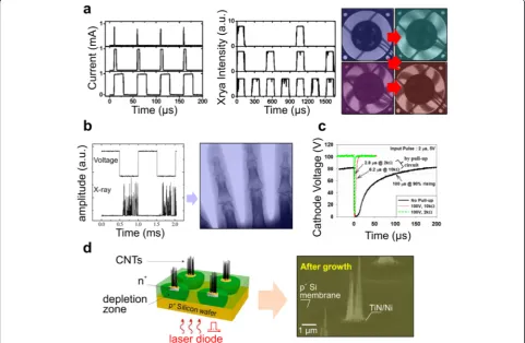
with only a very limited set of electronically controlled devices operating at frequencies in excess of a few hundred Hz to a few kHz [149,198,203,210]. The high-est electronic pulse rate achieved to date is of the order of 107 Hz, as reported by Cheng et al. [201]. Nevertheless, the pulse rate achieved by Thales [233] in their optically gated devices exceeds all other devices by a significant margin. Figure 6(a) shows the anode current and X-ray intensity temporal response by Reyes-Mena et al. [198]. Here the X-ray beam 0-90% turn-on time is <50μs and the system is used to image a rotating cooling fan. Images were acquired at a constant fan angular velocity with decreasing X-ray emis-sion pulse width. As the X-ray pulse width decreases the fan blade sharpness increases evidencing the usefulness of beam pulsing in acquiring high resolution images in mov-ing systems. The pulsmov-ing of the gate voltage has also been shown to produce turn on times of the order of 100 μs [149,198]. At an early stage, Yueet al.[149], as shown in
Figure 6Pulsed Sources. (a)Anode current and X-ray intensity temporal response plots showing an X-ray beam turn-on time of <50μs, and X-ray images of a rotating computer cooling fan acquired at a constant fan angular velocity with decreasing X-ray emission pulse width. Note the increased sharpness of the fan blades with increasingly rapid beam pulsing [198]. Copyright 2005, Joint Committee on Powder Diffraction Standards. (b)Bias voltage and X-ray emission temporal response plots with an acquired X-ray image of a users hand [149,156]. Copyright 2003, Elsevier and American Institute of Physics.(c)The time dependence of the cathode voltage with integrated pull-up resistance showing a rise time of <3μs [154]. Copyright 2013, SPIE.(d)Schematic depiction of a red-source photo-gated CNF-based electron source. Each vertically aligned CNF bundle sits on top of a pin+photodiode coated with a TiN diffusion barrier coated and a Ni catalyst, as illustrated in the scanning electron micrograph taken after the
Figure 6(b), demonstrated peak beam currents of up to 28 mA, at anode potentials of 14 kV, without degradation of the field emitters. An interesting artefact of their rapid pulsing was the chaotic and rather noisy X-ray emission, which showed an approximate periodicity of 100μS. The noise here must certainly be reduced if a practical device is to be realised.
The limiting factor in many pulsed systems is often the capacitance of the gate assembly. Kim et al. [154] showed that pulsing performance could be improved and demonstrated <3 μs pulse periods, as indicated by the cathode voltage, via the use of a simple high voltage MOSFET pull-up circuit to switch the cathode, proposing that their pulsed source may find application in angiog-raphy. However it is worth noting that such a measure does not correlate with the X-ray photon flux [198]. Liu
et al.[206], by pulsing the gate bias using a pulse gener-ator with a constant anode bias of 40 kV, showed a stable 0.3 mA temporal response over 15 h with an approximate pulse rise time of <5 ms. Certainly electronic control over the pulsing performance has some use. Though the band-width is dramatically reduced, by at least an order of mag-nitude, the on/off ratio can be increased and the emitter fabrication simplified. Nevertheless, this is necessarily at the expense of other technological challenges, chiefly the associated RC constant of the vacuum cavity. This RC constant induces intrinsic time delays that are not experienced in the optically stimulated case. As illus-trated in Figure 6(c), Kimet al. [154] employed 10 kΩ pull-up resistances to negate RC lag issues. The pulsing performance of arrayed sources has also been consid-ered. Wang et al. [169] showed millisecond temporal response in a matrix source designed for micro radio-therapy. This had an array of 5 × 10 pixels achieving an emission current of 3 mA per pixel.
In order to obviate issues associated with the devices RC time constants, as depicted in Figure 6(d), Thales Electron Devices exploited integrated photodiodes and direct optical excitation. Vertically aligned CNFs were grown on p-i-n+ photodiodes on a back etched Si membrane. The n+ doped areas were defined by ion implantation in a 5 μm thick intrinsic layer, whilst the p+ doped silicon wafer was subsequently thinned to obtain the 7 μm thick membrane [233]. These arrayed emitters where then irradiated, over the entire emitter area, with pulsed red laser light allowing them to at-tain very high bandwidth and on-off ratio of around 10, in addition to a maximum on current density of around 100 μA/cm2.
The availability of rapidly pulsed sources opens up the potential for high-speed, real-time inspection technologies, capable of coupling high throughput, on-line manufactur-ing with real-time inspection. Indeed, with controlled high pulse rates the potential to perform medical diagnostics
without strict patient restraints is accessed, allowing in-spection of dynamic organs without image blurring. Intrin-sic motion and the associated quasi-periodic respiration and heart beats, for example, allow one means of gating such high speed pulsed systems. One possible approach considered is to lock the gate electrode pulsing to the pa-tients’cardiac or respiration signal. Such motion-induced artefacts can thus be reduced as the X-ray exposure is syn-chronised with a patients physiological rhythm, or indeed an objects motion [206].
2.6.6 Static tomography & tomosynthesis
X-ray based Computed Tomography (CT) imaging is fundamental to medical diagnostics. However, at present such imaging devices are affected by long scan times. Enabled by advances in computer and detection tech-nologies, integration time issues are exacerbated when considered in relation to the concept of real-time 3D X-ray imaging. Multi-pixel sources offer one viable solution. Multi-pixel sources present a unique opportunity in next-generation inspection techniques, especially when one considers the physically small CNT FE cathodes, and the potential for nanoengineering and rapid switching. Pulsed multi-pixel sources give rise to a series of previously chal-lenging applications typically relating to real-time medical diagnostics [234]. Tomography relies on the acquisition of large numbers of images, whilst viewing a subject at a range of angles. These systems, at present, incorporate multiple sources which are sequentially switched. This al-lows the system to capture an array of independent images without the necessity to physically rotate components, pa-tients, or samples on an expensive and bulky gantry. The emerging alternative is to have multiple, distributed X-ray sources. Here, the subject remains stationary with the added benefit of more rapid data acquisition and poten-tially higher image quality. Indeed, such systems are largely immune to image blurring, which persists in conventional moving-source systems.
inter-emitter pitches of the order of a few tens of centi-metres. The system has also, rather impressively, demon-strated real-time 3D image reconstruction. Figure 7(b) shows another stationary computed tomography system by the same team. This system consists of 4 cathode banks, with a total of 52 separate cathode assemblies. Though ra-ther large and limited to stationary or slow moving objects, this prototype system is the first in a new wave of CNT-based real-time 3D tomosynthesis scanners.
High spatial resolution requires a small X-ray spot size. However, practical systems also require a wide field of view in order to be able to inspect suitably large areas. Thus, to realise high resolution large area scans the X-ray source must be constructed from multiple cathodes, each with dedicated focusing electrodes. One way to maximise the field of view is to carefully engineer the vacuum chamber to maximise the total angular field of view. A 5 pixel source system has been constructed by
Zhang et al. [236]. This system provided sequentially acquired images over a finite angular range, each fitted with an electrostatic focusing electrode to control the size and scanning of the focal spot, which had a width of less than 300μm. Operating at 40 kV, they showed that the electronic switching time was largely negligible with high emission reproducibility, both in FE curves and beam diameter, between the individual electron sources. Yanget al.demonstrated a multiple source digital breast tomosynthesis unit using an array of 25 cathodes, each individually programmed using analogue controls. Their sources employed CNT-based inks, each with a dedi-cated gate and an electrostatic focusing ring to control the focal spot size to approximately 200 μm [237]. In this system an impressive total angular field of view of up to 48° was realised, and the performance compared favourably with commercially available moving-source systems. A similar system, termed a multi-beam FE X-ray source, described a similar geometry [203]. A simple linear multiple source using an array of 31 CNT FE cathodes has also been constructed, for the purposes to digital breast tomosynthesis, which was shown to be capable of a total scan angle of 30° [171]. In a further extension, a digital chest tomosynthesis scanner was demonstrated [238]. This system used 75 CNT FE sources, operating at up to 80 kV with a 20° beam angle.
2.6.7 Multi-pixel sources
In the majority of the multi-pixel systems discussed the electron sources have largely been constructed using individual cathodes fabricated in linear arrays. A two dimensional geometry based on a series of linear arrays in a square or hexagonal format of physically separate detec-tors and sources, has been evaluated using simulation. Such a system is highly manufacturable [239], however; the inspection technique relies on close alignment of the generators and detectors which is likely challenging. Guzilovet al.[240] proposed circular arrays of FE emit-ters to emulate the classical rotary gantries used for CT, although their practical implementation has been
limited to staggered linear arrays. Two dimensional arrays have a number of advantages over their linear counterparts, chief amongst which is the potential for ad hoc beam shaping of the emergent X-rays. Micro-integration of two dimensional source arrays allows for ever higher spatial resolution and subsequent beam shaping. Such micro-integrated two dimensional FE source arrays have been realised, though only few such devices have been investigated. Figure 8(a) depicts a 5 × 10 electron beam array fabricated by Wanget al.[169], as mentioned above. Deposited using inking techniques (Figure 8(b)), the 50 individually addressable electron beams allow for arbitrarily defined, and controllable electron, and hence X-ray beam shapes, for application in radiotherapy. An example of one such ad hoc beam shaped, electronically defined, X-ray intensity distribution is illustrated in the bottom image of Figure 8(c). A dose rate of 1.24 Gy/min at the centre of the irradiated object was obtained at an emission current of 3.0 mA [169]. High energy sources for tomosynthesis based on such multi-pixel sources, with high anode potentials of up to 160 kV, have also been demonstrated by Sprengeret al.[241]. This was achieved using a square array of 4 × 13 electron sources for applications including image guided radiotherapy.
2.6.8 Compact & miniature sealed tubes
X-ray generators are often bulky devices, as a result of the thermal disspiation and subsequent cooling require-ments. Certain user specifications necessitate significant miniaturisation. Miniaturised sources find use in hand-held non-destructive testing, X-ray spectroscopy, elec-trically controlled brachytherapy and in situ radiation therapy. Miniature TE sources have been available for many years, but have proven challenging to miniaturise [242]. Amptek has launched a series of miniature X-ray sources [243]. Sealed FE sources, on the other hand, lend themselves to these applications, and in particular are well suited for portable X-ray applications. Though difficult to manufacture, miniaturised sources are emerging on the market place. As in the case of pulsed and


![Figure 9 Miniature CNT-based FE X-ray sources. (a)supporting current densities of up to 1 A/cmfiring of a CNT paste on the apex of a 0.6 mm Kovar rod, and operated at 12 kV [244]](https://thumb-us.123doks.com/thumbv2/123dok_us/849575.2079398/20.595.58.539.275.644/figure-miniature-sources-supporting-current-densities-cmfiring-operated.webp)
