Multilevel Sequential Logic Circuit Design
Avni Morgül
FSM Vakıf University, Biomedical Eng. Dept, Istanbul, Turkey Email: [email protected]
Fatma Sarıca
Maltepe University, Electrical & Electronics Eng. Dept., Istanbul, Turkey Email: [email protected]
Abstract—Multilevel logic circuits has advantages of simpler circuit complexity, less interconnections and small chip area. However it has not found enough attention and applications because there is not sufficient hardware available. Reference [1] proposes a multilevel flip-flop circuit and its applications for building counter circuits. In this paper it is shown that it is possible to design any arbitrary sequential logic circuit by using this flip-flop. The multilevel circuit is simpler and uses fewer transistors compared to the binary equivalent circuit.
Index Terms—multivalued logic, sequential logic, multivalued flip-flop, current mode CMOS logic
I. INTRODUCTION
Multilevel or multivalued logic circuits (MVL) may implement the logic operations more efficiently and faster by increasing the radix of the system or the number of levels used, in the expense of reduced noise margin. These systems become equivalent to an analog system if the radix is very large. So, it suffers from the noise and parameter variations of the components used in the realization.
The current mode design can be successfully applied to higher-radix or multi-valued logic circuit design, abbreviated as CM-MVL. Current-mode MVL structures
are presented in [11]Hata! Başvuru kaynağı
bulunamadı..
In current-mode design, the parameter variations of the components and the noise may result in incorrect logic levels may be obtained, if the number of cascaded stages exceeds a certain value. Therefore, it is unavoidable to restore the tabulated levels after a certain number of stages, unless the gates are self-restored type [12]. A new full-current mode CMOS-MVL restoration circuit is presented in [13].
II.
DEFINITIONSIn a radix-r multilevel system, any m-variable logic function, f(x1, x2,…, xm) may be represented in terms of basic operations, MIN, MAX and inverter. Here, each variable, xi , takes a value from the set R={0,1,…, r-1}.
Manuscript received November 14, 2013; revised March 1, 2014.
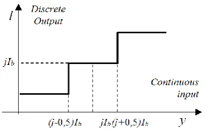
The radix, r, corresponds to the number of possible signal levels. In current mode MVL logic, levels are represented by current levels in terms of a base current, Ib. Thus, a variable x=0 is associated with the current level value,
I0=0, x=1 is associated with I1=Ib and so on. However, in
the circuits, a logic current level l, actually corresponds to an interval of the continuous quantity, y, such that
yl: {y (l – 05)Ib y ( l + 0.5)Ib} (1)
This means that a total parameter variation plus noise of ½Ib may be tolerated.
Figure 1. Conversion of continuous input signal to multilevel.
The definitions of basic MVL operations are given below [11].
MIN(x,y)=xy=xy
MAX(x,y)=xy=x+y
Complementof x :
1 x r x Truncated difference,
if 0 otherwise
x y x y
x y
The literal, (L)
otherwise
0 if ) ,
(k x k a x b L a b
k-CWC : x x k r
k
mod ) (
The upper and lower threshold operations
, :
0
c
u b
c if a b upper threshold th a
otherwise
, :
0
c
l b
c if a b lower threshold th a
otherwise
III. SEQUENTIAL CIRCUITS
It is known that the basic building blocks of sequential logic circuits are the flip-flops. Characteristic equations and next-state tables for conventional flip-flops such as
SR, JK, and T , for multilevel input signals are introduced in several studies [4]-[5].
Unfortunately, circuit level implementations of the equations are very complicated [6], [7] and they require the inversion of the current state output to calculate the next state. In current mode designs, inversion is performed by subtracting the current from the maximum allowable current [i.e. (r - 1)I0]. This operation increases the power consumption considerably. So, the inverter must be avoided for a low power design.
Since all standard flip-flop equations require inversion, it is decided to define a new flip-flop, which does not use any inverter. This new flip-flop is called AB flip-flop because it has two inputs, A and B, and the transition equation which does not have inverted terms, is stated as follows [1]:
Qn+1=A+B•Qn
The state transition table of the AB flip-flop is given in Table I. The flip-flop can successfully change its state for any input combination.
TABLE I. TRANSITION TABLE OF THE ABFLIP-FLOP
AB
Qn 00 01 02 03 10 11 12 13 20 21 22 23 30 31 32 33
0 0 0 0 0 1 1 1 1 2 2 2 2 3 3 3 3
1 0 1 1 1 1 1 1 1 2 2 2 2 3 3 3 3
2 0 1 2 2 1 1 2 2 2 2 2 2 3 3 3 3
3 0 1 2 3 1 1 2 3 2 2 2 3 3 3 3 3
Block diagram of the AB flip flop is given in Fig. 2. It is composed of a MIN circuit to perform AND operation, a MAX circuit to perform OR operation and a LATCH-RESTORER circuit to HOLD and restore the current state.
Figure 2. Block diagram of the AB flip-flop.
The MIN [14] and MAX [15] circuits are current-mode, multi-input circuits working based on winner/loser-takes-all principle as shown in Fig. 3. Although there are other simpler implementations of MIN and MAX circuits in the literature [4], this circuit is preferred because of its robustness. The LATCH/ RESTORER circuit is based on level restoration circuit design given in [13] and optimized for the new application to obtain smooth transitions. Since the current mode multilevel circuits are not self-restored the predefined current levels can be deviate from their original values due to some variations in active element dimensions, power supplies, technology parameters, etc. The signal must be restored to its original value before the variations exceeds ±Ib/2 value. In
addition, the flip-flop circuits have positive feedback in nature, which prohibits any variation from the predefined level. Otherwise, this variation forces the output to shift either to ground or power supply voltage. The restoration circuit is modified as LATCH/RESTORER circuit by adding a pass transistor properly. Both HOLD and restore operations performed at the same time by using the circuit given in Fig. 4.
Figure 3. (a) MIN and (b) MAX circuits [14], [15].
Figure 4. Modified latch and restoration circuit.
Timing of the flip flop circuit is performed by using
two-phase clock signals (clk, clk) which control the pass transistors of the latch circuit. The number of Q outputs (Iout) can be increased by adding more current mirrors to
the final stage. A
B A
Q
AB Flip-Flop
MAX
MIN
Latch Restorer
B
Q
7,5A clk
Iin 10A 2,5A 5A
clk Iout
VDD
IV. IMPLEMENTATION OF SEQUENTIAL CIRCUITS
Different type of sequential circuits, such as counters is designed by using the AB flip-flop, in order to show its usability.
A 1-digit modulo-4 counter is designed to test the new flip-flop. Then, the counter design work is extended to synchronous and asynchronous 2-digit modulo-16 counters. All these circuits are tested successfully [1]. A 4-level logic system is preferred (although most circuits are radix-free, minor modifications may needed to change/increase the logic levels for a 1-digit counter), in order to keep the noise margins in reasonable levels.
Using the counting diagram and state transition table of the flip-flop, we can obtain the next-state equation of the counter as follows, after necessary minimizations;
1 1 1 1 3 3 1 0 2 2 1 2 2 1 2
, 0
,
A Q B
A Q Q B Q Q
Here, 1
1
Q and 1
2
Q indicate 1-level clock-wise cyclic
operation and 3 1 3
Q and 2 1 0
Q are literal operations. The
3 1
3Q operation is logically equal to “detect if
3
1
Q ”, and
the 2
1 0
Q operation is logically equal to “detect if Q12”. So, we can replace the literal circuits with upper and lower threshold circuits, respectively. Threshold circuits are simpler and use fewer transistors than literal circuits. The complete block diagram of the synchronous 2-digit modulo-16 counter and simulation results are given in Fig. 5 and Fig. 6, respectively.
Figure 5. Synchronous 2-digit modulo-16 counter
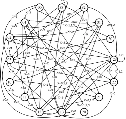
In order to show the suitability of the proposed new flip-flop, for any sequential multi-valued logic application, we propose and presented in this paper, an arbitrary state diagram for 1-input, 2-output quaternary logic circuit. HSPICE simulations show that circuit is working correctly.
Figure 6. Simulation result of 2-digit modulo-16 counter.
The state diagram of the circuit is given in Fig. 7. Using this state diagram, truth table is formed and introduced in
Table II. Here x is an input current, Q2 and Q1 are current state outputs and combined with x input to generate the excitation functions for A and B inputs of the flip-flops.
Q2+ and Q1+ are the calculated next state output levels.
00 32 02 03 10 23 22
12 13 20
21 31 01 11 33 X=0 X=2 X=1,2 X=1 X=1 X=2 X=1 X=1 X=1 X=0 X=0 X=0 X=0,1,2 X=0 X=0,1,2 X=0,1,2,3 X=0 X=3 X=3 X=3 X=2 X=2 X=2 X=2 X=1 X=1 X=1 X=0 X=0 X=0 X=3 X=0 X=0 X=3 X=3 X=3 X=3 X=3 X=3 X=3 X=2 X=2 X=2 X=3 X=1 X=1,2,3 X=0 X=2 X=1 30 X=1,2 X=3
Figure 7. State diagram of the sequential circuit.
TABLE II. TRUTH TABLE OF THE SEQUENTIAL CIRCUIT
In Present
State State Next FF Inputs In Present State State Next FF Inputs
x Q2 Q1 Q2+ Q1+ A1 B1 A2 B2 x Q2 Q1 Q2+ Q1+ A1 B1 A2 B2
0 0 0 1 1 1 0 1 0 2 0 0 3 1 1 0 3 0 0 0 1 1 2 2 1 1 0 2 0 1 3 2 2 0 3 0 0 0 2 1 3 3 2 1 0 2 0 2 3 3 3 0 3 0 0 0 3 1 3 0 3 1 0 2 0 3 3 0 0 0 3 0 0 1 0 1 1 1 0 1 0 2 1 0 3 1 1 1 3 0 0 1 1 1 2 2 1 1 1 2 1 1 3 2 2 1 3 1 0 1 2 1 3 3 2 1 1 2 1 2 3 3 3 1 3 1 0 1 3 1 3 0 3 1 1 2 1 3 3 1 0 1 3 1 0 2 0 0 1 1 0 0 0 2 2 0 0 1 1 2 0 0 0 2 1 1 2 2 1 0 1 2 2 1 1 2 2 2 0 1 0 2 2 1 3 3 2 0 1 2 2 2 2 3 3 2 0 2 0 2 3 1 3 0 3 0 1 2 2 3 2 2 0 2 0 2 0 3 0 0 1 1 0 0 0 2 3 0 0 1 1 3 0 0 0 3 1 1 2 2 1 0 1 2 3 1 1 2 2 3 0 1 0 3 2 1 3 3 2 0 1 2 3 2 2 3 3 3 0 2 0 3 3 1 3 0 3 0 1 2 3 3 3 3 0 3 0 3 1 0 0 2 1 1 0 2 0 3 0 0 0 1 1 0 0 0 1 0 1 2 2 2 1 2 0 3 0 1 0 2 2 0 0 0 1 0 2 2 3 3 2 2 0 3 0 2 0 3 3 0 0 0 1 0 3 2 3 0 3 2 0 3 0 3 0 0 0 0 0 0 1 1 0 2 1 1 0 2 0 3 1 0 0 1 1 1 0 0 1 1 1 2 2 2 1 2 1 3 1 1 0 2 2 1 0 0 1 1 2 2 3 3 2 2 1 3 1 2 0 3 3 1 0 0 1 1 3 2 3 0 3 2 1 3 1 3 0 1 0 1 0 0 1 2 0 0 1 1 0 0 0 3 2 0 0 1 1 2 0 0 1 2 1 1 2 2 1 0 1 3 2 1 0 2 2 2 0 0 1 2 2 2 3 3 2 0 2 3 2 2 0 3 3 2 0 0 1 2 3 2 3 0 3 0 2 3 2 3 0 2 0 2 0 0 1 3 0 0 1 1 0 0 0 3 3 0 0 1 1 3 0 0 1 3 1 1 2 2 1 0 1 3 3 1 0 2 2 3 0 0 1 3 2 2 3 3 2 0 2 3 3 2 0 3 3 3 0 0 1 3 3 2 3 0 3 0 2 3 3 3 0 3 0 3 0 0
Using this truth table, we obtain the input functions, by inspection, as follows (unfortunately there is not a simple method to simplify the multilevel logic equations).
A1Q11
LATCH
clk clk
clk clk
Lower threshold
clk
IN clk
OUT1 (LSD)
Q1 Q2
CWC B A AB ff Q Q Q
Q Upper threshold thL thU MIN clk LATCH CWC clk B A AB ff Q Q Q OUT2 (MSD)
B10x1Q
12x3Q2
A20Q 2 1x1
B2x1Q1Q2
Here, Q11 Indicates 1-level clock-wise cyclic operation. 1
0
x and 2x3 are literal operations [9]. They are logically equal to “detect if
x
1
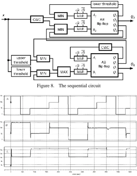
” and “detect if x2 ”,respectively. So, we can replace the literal circuits with upper and lower threshold circuits. Threshold circuits are simpler and use fewer transistors than literal circuits. The new sequential circuit can be designed as given in Fig. 8, by using these equations.
The circuit is tested for different input x currents, and the resulting output currents are shown in Figure 9. The results are totally compatible with the state diagram introduced in Fig. 7.
Figure 8. The sequential circuit
Figure 9. The input and output waveforms
V. CONCLUSION
In this study, we show that any sequential multi-valued logic circuit can be realized with the new multilevel AB flip-flop. An arbitrary state diagram for 4-level logic is drawn and it is realized by using the new flip-flop.
Future studies will be based on designing edge-triggered flip-flops rather than level edge-triggered ones. This will hopefully reduce the number of transistor used and will improve the speed considerably.
Another issue about multi-valued circuits is the minimization issue. Unfortunately there is no known method, which may be implemented easily, to simplify
the multilevel logic equations. The circuit designs will be less complicated with the effective minimization algorithms.
REFERENCES
[1] F. Sarica and A. Morgül, “AB-flip-flop, a first step to multilevel sequential logic”, Electronics Letters, pp: 310-312, Vol.47 No.5, 3 March 2011
[2] Y. Ota and B. M. Wilamowski, “Current-mode CMOS implementation of a fuzzy min-max network,” World Congress of Neural Networks, vol. 2, pp. 480-483, Washington DC, USA, 1995
[3] K. W. Current, “A CMOS quaternary latch,” in Proc. 19th International Symposium on Multiple Valued Logic, 1989, pp. 54-57.
[4] T. Temel and A. Morgül, “Implementation of multi-valued logic gates using full current-mode CMOS circuits,” Analog Integrated Circuits and Signal Processing, no. 39, pp. 191-204, Apr. 2004.
[5] J. I. Acha and J. L. Huertas, “General excitation table for a JK multistable,” Electronics Letters, vol. 11, Nos. 25/26, pp. 624, 1975
[6] K. Hirota and K. Ozawa, “The concept of fuzzy flip-flop,” IEEE Transactions on Systems, Man and Cybernetics, vol. 19, no. 5, pp. 980-997, 1989
[7] L. P. Maguire, T. M. McGinnity, and L. J. McDaid, “From a fuzzy flip-flop to a MVL flip-flop,” in Proc. 29th International Symposium on Multiple Valued Logic, 1999, pp. 294-299. [8] J. Diamond, W. Pedrycz, and D. McLeod, “Fuzzy JK flip-flops as
computational structures: Design and implementation,” IEEE Transactions on Circuits and Systems II- Analog and Digital Signal Processing, vol. 41, no. 3, pp. 215-226, 1994
[9] F. Sarica and A. Morgul, "Basic circuits for multi-valued sequential logic," Analog Integrated Circuits and Signal Processing, vol. 74, no. 1, pp. 91-96, Jan 2013.
[10] A. K. Jain, R. J. Bolton, and M. H. Abd-El Barr, "CMOS multiple-valued logic design,” Part I and II, IEEE Trans. Circuits and Systems, vol. 40, no. 8, pp. 503- 532, Aug. 1993.
[11] T. Temel and A. Morgul, “Implementation of multi-valued logic, simultaneous literal operations with full CMOS current-mode threshold circuits,” IEE Electronic Letters, vol. 38, no. 4, pp. 160-161, Feb. 14th 2002.
[12] D. H. Y. Teng and R. J. Bolton, “A self-restored current-mode CMOS multiple-valued Logic design architecture,” in Proc. IEEE Pacific Rim Conference on Communications, Computers and Signal Processing, 1999, pp. 436-439.
[13] A. Morgul and T. Temel, “Current-mode level restoration: Circuit for multi-valued logic,” Electronics Letters, vol. 41, no. 5, 3rd March 2005.
[14] C. Y. Huang, C. J. Wang, and B. D. Liu, “Modular current-mode multiple input minimum circuit for fuzzy logic controllers,”
Electronics Letters, vol. 32, no. 12, pp. 1067-1069, 1996. [15] I. Baturone, J. L. Huertas, A. Barriga, and S. Sánchez-Salono,
“Current-mode multiple-input max circuit,” Electronics Letters, vol. 30, no. 9, pp. 678-680, 1994.
Avni Morgul has been graduated from
![Figure 3. (a) MIN and (b) MAX circuits [14], [15].](https://thumb-us.123doks.com/thumbv2/123dok_us/9949623.1982827/2.595.327.519.348.673/figure-min-and-max-circuits.webp)